JP6028352B2 - Manufacturing method of power module substrate with heat sink - Google Patents
Manufacturing method of power module substrate with heat sink Download PDFInfo
- Publication number
- JP6028352B2 JP6028352B2 JP2012060687A JP2012060687A JP6028352B2 JP 6028352 B2 JP6028352 B2 JP 6028352B2 JP 2012060687 A JP2012060687 A JP 2012060687A JP 2012060687 A JP2012060687 A JP 2012060687A JP 6028352 B2 JP6028352 B2 JP 6028352B2
- Authority
- JP
- Japan
- Prior art keywords
- metal plate
- heat sink
- power module
- brazing
- ceramic substrate
- Prior art date
- Legal status (The legal status is an assumption and is not a legal conclusion. Google has not performed a legal analysis and makes no representation as to the accuracy of the status listed.)
- Active
Links
Images

Classifications
-
- H—ELECTRICITY
- H01—ELECTRIC ELEMENTS
- H01L—SEMICONDUCTOR DEVICES NOT COVERED BY CLASS H10
- H01L2224/00—Indexing scheme for arrangements for connecting or disconnecting semiconductor or solid-state bodies and methods related thereto as covered by H01L24/00
- H01L2224/01—Means for bonding being attached to, or being formed on, the surface to be connected, e.g. chip-to-package, die-attach, "first-level" interconnects; Manufacturing methods related thereto
- H01L2224/26—Layer connectors, e.g. plate connectors, solder or adhesive layers; Manufacturing methods related thereto
- H01L2224/31—Structure, shape, material or disposition of the layer connectors after the connecting process
- H01L2224/32—Structure, shape, material or disposition of the layer connectors after the connecting process of an individual layer connector
- H01L2224/321—Disposition
- H01L2224/32151—Disposition the layer connector connecting between a semiconductor or solid-state body and an item not being a semiconductor or solid-state body, e.g. chip-to-substrate, chip-to-passive
- H01L2224/32221—Disposition the layer connector connecting between a semiconductor or solid-state body and an item not being a semiconductor or solid-state body, e.g. chip-to-substrate, chip-to-passive the body and the item being stacked
- H01L2224/32225—Disposition the layer connector connecting between a semiconductor or solid-state body and an item not being a semiconductor or solid-state body, e.g. chip-to-substrate, chip-to-passive the body and the item being stacked the item being non-metallic, e.g. insulating substrate with or without metallisation
-
- H—ELECTRICITY
- H01—ELECTRIC ELEMENTS
- H01L—SEMICONDUCTOR DEVICES NOT COVERED BY CLASS H10
- H01L2224/00—Indexing scheme for arrangements for connecting or disconnecting semiconductor or solid-state bodies and methods related thereto as covered by H01L24/00
- H01L2224/01—Means for bonding being attached to, or being formed on, the surface to be connected, e.g. chip-to-package, die-attach, "first-level" interconnects; Manufacturing methods related thereto
- H01L2224/42—Wire connectors; Manufacturing methods related thereto
- H01L2224/47—Structure, shape, material or disposition of the wire connectors after the connecting process
- H01L2224/48—Structure, shape, material or disposition of the wire connectors after the connecting process of an individual wire connector
- H01L2224/4805—Shape
- H01L2224/4809—Loop shape
- H01L2224/48091—Arched
-
- H—ELECTRICITY
- H01—ELECTRIC ELEMENTS
- H01L—SEMICONDUCTOR DEVICES NOT COVERED BY CLASS H10
- H01L2224/00—Indexing scheme for arrangements for connecting or disconnecting semiconductor or solid-state bodies and methods related thereto as covered by H01L24/00
- H01L2224/01—Means for bonding being attached to, or being formed on, the surface to be connected, e.g. chip-to-package, die-attach, "first-level" interconnects; Manufacturing methods related thereto
- H01L2224/42—Wire connectors; Manufacturing methods related thereto
- H01L2224/47—Structure, shape, material or disposition of the wire connectors after the connecting process
- H01L2224/48—Structure, shape, material or disposition of the wire connectors after the connecting process of an individual wire connector
- H01L2224/481—Disposition
- H01L2224/48151—Connecting between a semiconductor or solid-state body and an item not being a semiconductor or solid-state body, e.g. chip-to-substrate, chip-to-passive
- H01L2224/48221—Connecting between a semiconductor or solid-state body and an item not being a semiconductor or solid-state body, e.g. chip-to-substrate, chip-to-passive the body and the item being stacked
- H01L2224/48225—Connecting between a semiconductor or solid-state body and an item not being a semiconductor or solid-state body, e.g. chip-to-substrate, chip-to-passive the body and the item being stacked the item being non-metallic, e.g. insulating substrate with or without metallisation
- H01L2224/48227—Connecting between a semiconductor or solid-state body and an item not being a semiconductor or solid-state body, e.g. chip-to-substrate, chip-to-passive the body and the item being stacked the item being non-metallic, e.g. insulating substrate with or without metallisation connecting the wire to a bond pad of the item
-
- H—ELECTRICITY
- H01—ELECTRIC ELEMENTS
- H01L—SEMICONDUCTOR DEVICES NOT COVERED BY CLASS H10
- H01L2224/00—Indexing scheme for arrangements for connecting or disconnecting semiconductor or solid-state bodies and methods related thereto as covered by H01L24/00
- H01L2224/73—Means for bonding being of different types provided for in two or more of groups H01L2224/10, H01L2224/18, H01L2224/26, H01L2224/34, H01L2224/42, H01L2224/50, H01L2224/63, H01L2224/71
- H01L2224/732—Location after the connecting process
- H01L2224/73251—Location after the connecting process on different surfaces
- H01L2224/73265—Layer and wire connectors
Description
本発明は、大電流、高電圧を制御するパワーモジュールを構成するヒートシンク付パワーモジュール用基板の製造方法に関する。 The present invention relates to a high current, producing how the substrate for a power module with a heat sink which constitutes a power module for controlling the high voltage.
従来、大電流、高電圧を制御する半導体装置として、半導体チップ等の電子部品をパワーモジュール用基板上に搭載した構成のパワーモジュールが知られている。パワーモジュールを製造する方法として、例えば、特許文献1および特許文献2に記載された方法が知られている。これらの製造方法では、まずセラミックス基板の一方の面にAl−Si系等のろう材を介して回路層となる金属板を積層し、セラミックス基板の他方の面にろう材を介して放熱層となる金属板を積層して、これらを積層方向に加圧するとともに加熱し、セラミックス基板と各金属板とを接合し、パワーモジュール用基板を製造する。次いで、放熱層の、セラミックス基板が接合されている面とは反対側の面に、ろう材を介してヒートシンクの天板部を積層し、この積層方向に加圧するとともに加熱して放熱層とヒートシンクとを接合することにより、ヒートシンク付パワーモジュール用基板が製造される。 2. Description of the Related Art Conventionally, as a semiconductor device that controls a large current and a high voltage, a power module having a configuration in which an electronic component such as a semiconductor chip is mounted on a power module substrate is known. As a method for manufacturing a power module, for example, methods described in Patent Document 1 and Patent Document 2 are known. In these manufacturing methods, first, a metal plate to be a circuit layer is laminated on one surface of a ceramic substrate via a brazing material such as Al-Si, and a heat radiation layer and a heat dissipation layer are disposed on the other surface of the ceramic substrate via a brazing material. These metal plates are laminated, pressed and heated in the laminating direction, and the ceramic substrate and each metal plate are joined together to produce a power module substrate. Next, the top plate of the heat sink is laminated on the surface of the heat dissipation layer opposite to the surface to which the ceramic substrate is bonded via a brazing material, and the heat dissipation layer and the heat sink are heated by pressing and heating in this laminating direction. Are joined together to produce a power module substrate with a heat sink.
ヒートシンクとパワーモジュール用基板の金属板との間の接合方法としては、ろう付け、はんだ付け、ねじ止め、フラックスを用いたろう付け法などが適用される。特許文献3では、ヒートシンクの天板とパワーモジュール用基板の金属層との接合方法として、フラックスを塗布したろう付法が記載されている。このフラックスを用いたろう付法では、例えば、フッ化物系のフラックスをろう材面に塗布してろう材面の酸化物を除去し、非酸化性雰囲気中で加熱して接合するろう付法であり、高価な設備が不要で、比較的容易に安定したろう付が可能である。 As a joining method between the heat sink and the metal plate of the power module substrate, brazing, soldering, screwing, a brazing method using a flux, or the like is applied. Patent Document 3 describes a brazing method in which a flux is applied as a method of joining the top plate of the heat sink and the metal layer of the power module substrate. The brazing method using this flux is, for example, a brazing method in which a fluoride-based flux is applied to the brazing material surface to remove oxides on the brazing material surface and heated in a non-oxidizing atmosphere to join. Expensive equipment is unnecessary and stable brazing can be performed relatively easily.
しかしながら、パワーモジュールの製造過程において、パワーモジュール用基板の金属板とヒートシンクとをフラックスを用いたろう付を行う際に、金属板とヒートシンクとの間から流出したフラックスが金属板の側面を経由してセラミックス基板と金属板との接合部界面に引き込まれてこの接合部を侵食してしまうと、これにより接合部にクラックが生じ、セラミックス基板と金属板との剥離が生じやすくなるおそれがある。 However, during the power module manufacturing process, when the metal plate of the power module substrate and the heat sink are brazed using a flux, the flux that flows out between the metal plate and the heat sink passes through the side surface of the metal plate. If the joint is drawn into the joint interface between the ceramic substrate and the metal plate and erodes the joint, a crack may occur in the joint, and the ceramic substrate and the metal plate may be easily separated.
本発明は、このような事情に鑑みてなされたもので、セラミックス基板と金属板との接合部に剥離を生じさせることなく、金属板とヒートシンクとをフラックスを用いてろう付し、接合信頼性の高いヒートシンク付パワーモジュール用基板を提供することを目的とする。 The present invention has been made in view of such circumstances, and brazing the metal plate and the heat sink using a flux without causing separation at the joint portion between the ceramic substrate and the metal plate, thereby improving the bonding reliability. An object of the present invention is to provide a power module substrate with a high heat sink.
本発明者は、金属板の側面を経由するフラックスの移動について鋭意研究した結果、次の知見を得た。
パワーモジュール用基板の製造過程において、セラミックス基板と金属板とのろう付時に、接合に寄与しない余剰分のろう材が接合部から押し出され、金属板の側面に付着する場合がある。この一次ろう付工程で金属板側面に付着したろう材が固化し、金属板側面の表面に網目状の溝が形成され易く、このような状態で金属板とヒートシンクとをノコロックろう付すると、金属板とヒートシンクとの間から流出したフラックスが、金属板の側面に付着したろう材に接触し、この網目状の溝を伝って流動してセラミックス基板と金属板との接合部界面に引き込まれる。したがって、フラックスの侵食によるセラミックス基板と金属板との剥離を防止するには、このフラックスのろう材表面での流動を防止する必要がある。本発明は、このような知見の下、以下の解決手段とした。
As a result of earnest research on the movement of the flux via the side surface of the metal plate, the present inventor has obtained the following knowledge.
In the manufacturing process of the power module substrate, when the ceramic substrate and the metal plate are brazed, an excessive amount of brazing material that does not contribute to the bonding may be pushed out from the bonded portion and adhere to the side surface of the metal plate. In this primary brazing process, the brazing material adhering to the side surface of the metal plate is solidified, and a mesh-like groove is easily formed on the surface of the side surface of the metal plate. The flux flowing out from between the plate and the heat sink comes into contact with the brazing material adhering to the side surface of the metal plate, flows through this mesh-like groove, and is drawn into the interface between the ceramic substrate and the metal plate. Therefore, in order to prevent peeling of the ceramic substrate and the metal plate due to erosion of the flux, it is necessary to prevent the flux from flowing on the surface of the brazing material. Based on such knowledge, the present invention is set as the following solution.
すなわち、本発明のヒートシンク付パワーモジュール用基板の製造方法は、ヒートシンクと、このヒートシンクに接合される金属板がセラミックス基板の表面に接合されてなるパワーモジュール用基板とを接合してヒートシンク付パワーモジュール用基板を製造する方法であって、前記金属板のセラミックス基板接合面と前記セラミックス基板との間をろう材を用いてろう付けして前記パワーモジュール用基板を形成する一次ろう付工程と、前記金属板のヒートシンク接合面と前記ヒートシンクとをフラックスを用いたろう付により接合する二次ろう付工程とを有し、前記二次ろう付工程の前に、前記金属板の側面を研磨することにより、前記一次ろう付工程により前記金属板の側面に付着したろう材を除去することを特徴とする。 That is, in the method for manufacturing a power module substrate with a heat sink according to the present invention, a power module with a heat sink is formed by bonding a heat sink and a power module substrate in which a metal plate bonded to the heat sink is bonded to the surface of the ceramic substrate. A method of manufacturing a power substrate, wherein the power module substrate is formed by brazing between a ceramic substrate bonding surface of the metal plate and the ceramic substrate using a brazing material; and A secondary brazing step of joining the heat sink joint surface of the metal plate and the heat sink by brazing using a flux, and polishing the side surface of the metal plate before the secondary brazing step , The brazing material adhering to the side surface of the metal plate is removed by the primary brazing process .
この製造方法によれば、二次ろう付工程の前に金属板側面を研磨しているので、一次ろう付工程において金属板の側面に付着した余剰のろう材の少なくとも表面部が研磨により除去されることにより、金属板の側面が平坦になり、その結果、二次ろう付工程においてフラックスが金属板とヒートシンクとの間から流出したとしても、金属板の側面を伝ってセラミックス基板と金属板との接合部まで到達することが防止される。 According to this manufacturing method, since the metal plate side surface is polished before the secondary brazing step, at least the surface portion of the excess brazing material adhering to the side surface of the metal plate is removed by polishing in the primary brazing step. As a result, even if the flux flows out from between the metal plate and the heat sink in the secondary brazing process, the side surface of the metal plate becomes flat along the side surface of the metal plate. Reaching the joint portion is prevented.
また、この製造方法において、金属板の側面をブラスト処理によって研磨することが望ましい。金属板の側面に一次ろう付工程によって形成された網目状の溝は、余剰ろう材が固化して形成されたものであるから、ブラスト処理によって簡便に除去することができる。 In this manufacturing method, it is desirable to polish the side surface of the metal plate by blasting. The mesh-like grooves formed on the side surfaces of the metal plate by the primary brazing step are formed by solidifying the excess brazing material, and can be easily removed by blasting.
本発明のパワーモジュール用基板は、ヒートシンクに接合される金属板がセラミックス基板の表面に接合されてなり、前記金属板の側面の算術平均粗さRaが0.7μm以下に形成されているとよい。
金属板にろう材が付着していたとしても、その表面が算術平均粗さRaで0.7μm以下の平坦面であれば、ヒートシンクを接合する際にフラックスが金属板側面を伝ってセラミックス基板との接合部内に引き込まれることが防止される。
The power module substrate of the present invention may the metal plate to be joined to the heat sink is joined to the surface of the ceramic substrate, an arithmetic mean roughness Ra of the side surface of the metal plate is formed below 0.7μm .
Even if the brazing material is attached to the metal plate, if the surface is a flat surface with an arithmetic average roughness Ra of 0.7 μm or less, the flux is transmitted along the side surface of the metal plate when the heat sink is joined. It is prevented from being drawn into the joint portion.
本発明のヒートシンク付パワーモジュール用基板の製造方法およびパワーモジュール用基板によれば、ヒートシンクとパワーモジュール用基板との接合の際に用いられるフラックスがセラミックス基板と金属板との接合部に引き込まれることが防止され、セラミックス基板と金属板との接合部に剥離を生じさせず、接合信頼性の高いヒートシンク付パワーモジュール用基板を提供することができる。 According to the method for manufacturing a power module substrate with a heat sink and the power module substrate of the present invention, the flux used when the heat sink and the power module substrate are bonded is drawn into the bonded portion between the ceramic substrate and the metal plate. Therefore, it is possible to provide a power module substrate with a heat sink having high bonding reliability without causing peeling at the bonding portion between the ceramic substrate and the metal plate.
以下、本発明の実施形態について、図面を参照しながら説明する。
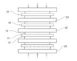
図1は、本実施形態のパワーモジュール用基板10を用いたパワーモジュール100を示している。このパワーモジュール100は、パワーモジュール用基板10と、パワーモジュール用基板10の表面に搭載された半導体チップ等の電子部品20と、この電子部品20とは反対面でパワーモジュール用基板10に接合されたヒートシンク30とから構成される。
Hereinafter, embodiments of the present invention will be described with reference to the drawings.
FIG. 1 shows a
パワーモジュール用基板10は、セラミックス基板11と、セラミックス基板11の両面に積層された金属板12,13とを備える。このパワーモジュール用基板10において、セラミックス基板11の一方の表面に積層された金属板12は回路層となり(以下、この金属板12を回路層用金属板という場合がある)、その表面に電子部品20がはんだ付けされる。また、他方の金属板13は放熱層とされ(以下、この金属板13を放熱層用金属板という場合がある)、その表面にヒートシンク30が取り付けられる。
The
セラミックス基板11は、例えば、AlN(窒化アルミニウム)、Si3N4(窒化珪素)等の窒化物系セラミックス、もしくはAl2O3(アルミナ)等の酸化物系セラミックスにより形成され、その厚さは0.2〜1.5mmの範囲内に設定されており、本実施形態では、0.635mmに設定されている。
The
回路層用金属板12は、純度99質量%以上のアルミニウムが用いられ、JIS規格では、1000番台のアルミニウム、特に1N90(純度99.9質量%以上:いわゆる3Nアルミニウム)または1N99(純度99.99質量%以上:いわゆる4Nアルミニウム)を用いることができる。放熱層用金属板13は、純度99質量%以上のアルミニウムが用いられ、JIS規格では、1000番台のアルミニウム、特に1N99(純度99.99質量%以上:いわゆる4Nアルミニウム)を用いることができる。なお、本実施形態では、図1に示すように、セラミック基板11の平面寸法は、回路層12及び金属層13の平面寸法より大きく設定されている。
Aluminum having a purity of 99% by mass or more is used for the
このパワーモジュール用基板10においては、放熱層用金属板13に熱サイクル時のセラミックス基板11とヒートシンク30との間の熱伸縮差に対する緩衝機能を持たせたるため、回路層用金属板12よりも肉厚に形成されたものを用いている。例えば、回路層用金属板12の厚さは600μm、放熱層用金属板13の厚さは1600μmである。また、放熱層用金属板13には、純度の高いアルミニウム(例えば1N99)を用いるのが好ましい。
In this
そして、これら金属板12,13とセラミックス基板11とは、ろう付けにより接合されている。ろう材としては、Al−Si系、Al−Ge系、Al−Cu系、Al−Mg系またはAl−Mn系等の合金が使用される。
And these
放熱層用金属板13の表面(ヒートシンク接合面)13aには、複数本の溝14が相互に平行に形成されている。これら溝14は、平面視矩形の金属板13の一方の側縁から他方の側縁にかけて平行に形成されている。溝14は、横断面がV字状やU字状となっている。
A plurality of
ヒートシンク30としては、板状の放熱板、内部に冷媒が流通する冷却器、フィンが形成された液冷、空冷放熱器、ヒートパイプなど、熱の放散によって温度を下げることを目的とした金属部品が含まれる。よって、平板状のもの、熱間鍛造等によって多数のピン状フィンを一体に形成したもの、押出成形によって相互に並行な流路を一体に形成したものなど、その形状等は特に限定されない。また、その材料は、熱伝導が良好な材質、例えばA6000台のアルミニウム合金により形成される。図示例では、冷却媒体(例えば冷却水)を流通させるための複数の流路30aが相互に並行に形成されている。このヒートシンク30とパワーモジュール用基板10の放熱層用金属板13とはろう付けにより接合され、ろう材としては、Al−Si系、Al−Ge系、Al−Cu系、Al−Mg系またはAl−Mn系等の合金が用いられる。
As the heat sink 30, a metal part intended to lower the temperature by heat dissipation, such as a plate-like heat sink, a cooler in which a refrigerant flows inside, a liquid cooling with fins formed, an air-cooled heat sink, a heat pipe, etc. Is included. Therefore, the shape and the like of the flat plate, the one in which a large number of pin-shaped fins are integrally formed by hot forging, the one in which flow paths parallel to each other are integrally formed by extrusion are not particularly limited. The material is formed of a material having good heat conduction, for example, A6000 aluminum alloys. In the illustrated example, a plurality of
なお、回路層用金属板12と電子部品20との接合には、Sn−Ag−Cu系,Zn−Al系もしくはPb−Sn系等のはんだ材が用いられる。図1中符号21がそのはんだ接合層を示す。また、電子部品20と金属板12の端子部との間は、アルミニウムからなるボンディングワイヤ22により接続される。
For joining the circuit
このパワーモジュール用基板10は、セラミックス基板11と各金属板12,13を接合することにより形成される。
具体的には、まず、金属板12,13を、シート材からプレス加工により形成する。この場合、回路層用金属板12は単にシート材から打ち抜くことにより形成される。一方、放熱層用金属板13は、シート材に複数の溝14を形成した後に打ち抜き加工される。溝14は、シート材の金属板13となる領域をカバーする範囲にパンチを押圧することにより形成される。
The
Specifically, first, the
次に、溝14を形成した放熱層用金属板13の溝14が形成されていない表面(セラミックス基板接合面)13bにろう材を介してセラミックス基板11を積層し、このセラミックス基板11の上にろう材を介して回路層用金属板12を積層する。この場合、ろう材は、金属板12,13をシート材からプレス加工により打ち抜く際にシート材にろう材箔を貼付しておき、このろう材箔ごと打ち抜くことにより、ろう材箔が貼付された金属板12,13を形成するとよい。
そして、これら積層したセラミックス基板11および各金属板12,13を厚さ方向に加圧しながら真空雰囲気中で加熱することによりろう付けする(一次ろう付工程)。
Next, a
Then, the laminated
この一次ろう付工程においては、図2に示すように、セラミックス基板11および両金属板12,13からなるユニットを多数組積層するとともに、各ユニットの間にカーボン板、グラファイト板等からなるクッション層23を配置し、これらを積層状態で加圧、加熱する。この時の加圧力は0.1〜2.5MPa、加熱温度は630〜655℃、加熱時間は1〜60分とする。このろう付け工程において、セラミックス基板11と金属板12,13との間のろう材が溶融して両者を固着することにより、パワーモジュール用基板10が形成される。
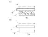
このとき、セラミックス基板11と金属板13との間からろう材が漏れ出ると、金属板13の側面13cに付着する。図3(a)は、その金属板13の側面13cにろう材が付着した状態を模式的に示しており、ろう材の表面に網目状の溝が形成される。
In this primary brazing process, as shown in FIG. 2, a plurality of units each composed of a
At this time, if the brazing material leaks from between the
次に、この金属板13の側面13cをブラスト研磨する。
このブラスト研磨に際しては、金属板13の側面13c以外のパワーモジュール用基板10の表面(金属板13の溝14が形成されている面、セラミックス基板11の表面)をマスキングしておき、ノズルから圧縮空気とともに投射材(研磨材)を噴射して、金属板13の側面13cに吹き付ける。投射材としては例えば平均粒径28μm〜32μmのSiCの粉末が用いられ、投射速度は、金属板13の側面13cにおける加圧力として0.15MPa〜0.20MPaとされる。
そして、このブラスト研磨により、金属板13の側面13cは、算術平均粗さRaが0.7μm以下に仕上げられ、これにより、金属板13の側面13cに付着していたろう材は除去される。図3(b)はブラスト研磨した後の金属板13の側面を示しており、ろう材により形成されていた網目状の溝は除去され、平滑な表面に仕上げられる。
Next, the
In this blast polishing, the surface of the
By this blast polishing, the
次に、金属板13とヒートシンク30とをノコロックろう付け法により接合して、パワーモジュール用基板10とヒートシンク30とを接合する(二次ろう付工程)。ノコロックろう付け法は、ろう材面に金属表面の酸化物を除去するフッ化物系フラックスを塗布して、非酸化性雰囲気(例えばN2雰囲気)中で600〜615℃に加熱して、ろう付けする方法である。
Next, the
フラックスには、KAlF4、K2AlF5、K3AlF6等が用いられる。金属板13とヒートシンク30とを接合するろう材は、例えばAi−Si系合金が用いられ、ヒートシンク30の表面に予めクラッドされているか、ろう材箔の形態でヒートシンク30に重ねることにより供給される。
As the flux, KAlF 4 , K 2 AlF 5 , K 3 AlF 6 or the like is used. The brazing material that joins the
この二次ろう付工程において、ヒートシンク30と接合される金属板13のヒートシンク接合面13aに複数の溝14が形成されていることにより、ろう付け時のフラックスは、ガス状となって各溝14を通ってヒートシンク30と金属板13との間から外部に流出する。したがって、フラックスは金属板13とヒートシンク30との間に滞留することが抑制され、ろう付け後にボイドとして残存することが防止される。
一方、外部に流出したフラックスは、金属板13の側面13cでは一次ろう付工程で付着したろう材が除去され、算術平均粗さRaが0.7μm以下の平坦面に仕上げられているので、この金属板13の側面13cの下部に一部が付着したとしても、この側面13cを這い上がることはなく、そのほとんどがガスとして外部に放出される。したがって、金属板13とセラミックス基板11との接合部をフラックスが侵食することが防止され、これにより、金属板13とセラミックス基板11とに剥離が生じることを防止することができる。
In this secondary brazing process, a plurality of
On the other hand, the flux that has flowed to the outside is removed from the brazing material attached in the primary brazing process on the
以上説明したように、このヒートシンク付パワーモジュール用基板の製造方法によれば、セラミックス基板と金属板との接合部に剥離を生じさせず、接合信頼性の高いヒートシンク付パワーモジュール用基板を提供することができる。 As described above, according to this method for manufacturing a power module substrate with a heat sink, there is provided a power module substrate with a heat sink having high bonding reliability without causing separation at the bonded portion between the ceramic substrate and the metal plate. be able to.
次に、本発明の効果確認のために、以下の実験を行った。
32mm×32mmの窒化アルミニウムからなるセラミックス基板の上面に30mm×30mm、厚さ0.6mmの純アルミニウム(1N99)からなる回路層用金属板、下面に28mm×28mm、厚さ1.6mmの純アルミニウム(1N99)からなる放熱層用金属板を、厚さ15μmのAl−7.5質量%Siろう材を用いて真空中で640℃、0.49MPa(5kgf/cm2)で加圧しながら接合して、パワーモジュール用基板を作製した。
Next, in order to confirm the effect of the present invention, the following experiment was performed.
Circuit board metal plate made of pure aluminum (1N99) of 30 mm x 30 mm and thickness of 0.6 mm on the upper surface of a ceramic substrate made of 32 mm x 32 mm aluminum nitride, and pure aluminum of 28 mm x 28 mm and thickness of 1.6 mm on the lower surface A metal plate for a heat dissipation layer made of (1N99) was bonded using a 15 μm thick Al-7.5 mass% Si brazing material in a vacuum at 640 ° C. and 0.49 MPa (5 kgf / cm 2). A power module substrate was prepared.
このパワーモジュール用基板に対して、放熱層用金属板の側面を表1に示す表面状態とした。表1のうち、試料1〜試料3は、金属板の側面をブラスト研磨し、試料4は、金属板の側面をブラスト研磨しなかったものである。その後、ノコロックフラックス(森田化学製FL−7)とAl−Siろう材を用いて窒素雰囲気中でノコロックろう付法により放熱層用金属板に厚さ5mmのA6063材からなるヒートシンクを接合した。
これらのサンプルについて、冷熱サイクル試験として、−40℃から125℃に10分間で上昇させ、125℃に15分保持した後、125℃から−40℃に10分間で下降させ、−40℃に15分保持する温度履歴を1サイクルとした冷熱サイクルを3000サイクル付与し、セラミックス基板と放熱層用金属板との接合界面の剥離による接合欠陥率を評価した。
With respect to this power module substrate, the side surface of the heat dissipation layer metal plate was in the surface state shown in Table 1. In Table 1, Sample 1 to Sample 3 are blast polished on the side surface of the metal plate, and Sample 4 is one in which the side surface of the metal plate is not blast polished. Thereafter, a heat sink made of A6063 having a thickness of 5 mm was joined to the metal plate for the heat-dissipating layer by a noco-lock brazing method in a nitrogen atmosphere using noco-rock flux (FL-7 manufactured by Morita Chemical) and an Al-Si brazing material.
For these samples, as a thermal cycle test, the temperature was raised from −40 ° C. to 125 ° C. over 10 minutes, held at 125 ° C. for 15 minutes, then lowered from 125 ° C. to −40 ° C. over 10 minutes, and then moved to −40 ° C. for 15 minutes. A cooling cycle with a temperature history of 1 minute was given as 3000 cycles, and the bonding defect rate due to peeling of the bonding interface between the ceramic substrate and the metal plate for the heat dissipation layer was evaluated.
接合欠陥率は、超音波探傷装置を用いて接合部を評価し、接合すべき面積に対する剥離面積(接合欠陥率=剥離面積/接合すべき面積)により算出した。接合すべき面積は放熱層用金属板の面積である。また、超音波探傷像において、剥離は接合部内の白色部で示されることから、この白色部の面積を剥離面積とした。この場合、円相当で1mmφ以上接合されていない部位(非接合部とする)が認められた場合を剥離とし、接合面全体に占める非接合部の面積比率を測定した。この接合欠陥率を二次接合工程直後(初期)と冷熱サイクル試験後でそれぞれ測定した。
その結果を表1に示す。表1において、評価は、接合欠陥率が25%以上となったものを×、15%以上25%未満を△、15%未満を○とした。
The bonding defect rate was calculated by evaluating a bonded portion using an ultrasonic flaw detector and calculating a peeled area with respect to an area to be bonded (bonding defect rate = peeled area / area to be bonded). The area to be joined is the area of the metal plate for the heat dissipation layer. Further, in the ultrasonic flaw detection image, since peeling is indicated by a white portion in the joint portion, the area of the white portion is defined as a peeling area. In this case, the case where a portion equivalent to a circle and not joined by 1 mmφ or more (referred to as a non-joined portion) was recognized as peeling, and the area ratio of the non-joined portion in the entire joint surface was measured. The bonding defect rate was measured immediately after the secondary bonding step (initial stage) and after the thermal cycle test.
The results are shown in Table 1. In Table 1, the evaluation was evaluated as x when the bonding defect rate was 25% or more, Δ when 15% or more and less than 25%, and ○ when less than 15%.

表1から明らかなように、ブラスト研磨を行った試料1から試料3は、金属板の側面にろう材により形成された網目状の溝は除去され、その算術平均粗さRaが0.7μm以下となっており、接合初期及び冷熱サイクル後においても、いずれも接合欠陥率は小さくなった。一方、ブラスト研磨を行っていない試料4は、接合初期及び冷熱サイクル後のいずれにおいても試料1〜3と比較して劣化していることが確認できた。 As is clear from Table 1, in Samples 1 to 3 subjected to blast polishing, the mesh-like grooves formed of the brazing material on the side surfaces of the metal plate were removed, and the arithmetic average roughness Ra was 0.7 μm or less. As a result, the bonding defect rate was small both in the initial stage of bonding and after the thermal cycle. On the other hand, it was confirmed that the sample 4 not subjected to blast polishing was deteriorated as compared with the samples 1 to 3 both in the initial stage of bonding and after the cooling and heating cycle.
なお、本発明は前記実施形態の構成のものに限定されるものではなく、細部構成においては、本発明の趣旨を逸脱しない範囲において種々の変更を加えることが可能である。
実施形態では、一次接合工程で金属板の側面に付着したろう材をブラスト研磨により除去したが、金属板の側面を研磨するものであれば、化学研磨、電解研磨、バフ研磨などを用いることもできる。
In addition, this invention is not limited to the thing of the structure of the said embodiment, In a detailed structure, it is possible to add a various change in the range which does not deviate from the meaning of this invention.
In the embodiment, the brazing material adhering to the side surface of the metal plate in the primary bonding step is removed by blast polishing, but chemical polishing, electrolytic polishing, buffing, etc. may be used as long as the side surface of the metal plate is polished. it can.
10 パワーモジュール用基板
11 セラミックス基板
12 金属板(回路層用金属板)
13 金属板(放熱層用金属板)
13a ヒートシンク接合面
13b セラミックス基板接合面
13c 側面
14 溝
20 電子部品
21 はんだ接合層
22 ボンディングワイヤ
23 クッション層
30 ヒートシンク
30a 流路
100 パワーモジュール
10
13 Metal plate (metal plate for heat dissipation layer)
13a Heat sink
Claims (1)
Priority Applications (1)
| Application Number | Priority Date | Filing Date | Title |
|---|---|---|---|
| JP2012060687A JP6028352B2 (en) | 2012-03-16 | 2012-03-16 | Manufacturing method of power module substrate with heat sink |
Applications Claiming Priority (1)
| Application Number | Priority Date | Filing Date | Title |
|---|---|---|---|
| JP2012060687A JP6028352B2 (en) | 2012-03-16 | 2012-03-16 | Manufacturing method of power module substrate with heat sink |
Publications (2)
| Publication Number | Publication Date |
|---|---|
| JP2013197185A JP2013197185A (en) | 2013-09-30 |
| JP6028352B2 true JP6028352B2 (en) | 2016-11-16 |
Family
ID=49395820
Family Applications (1)
| Application Number | Title | Priority Date | Filing Date |
|---|---|---|---|
| JP2012060687A Active JP6028352B2 (en) | 2012-03-16 | 2012-03-16 | Manufacturing method of power module substrate with heat sink |
Country Status (1)
| Country | Link |
|---|---|
| JP (1) | JP6028352B2 (en) |
Families Citing this family (3)
| Publication number | Priority date | Publication date | Assignee | Title |
|---|---|---|---|---|
| JP5954371B2 (en) * | 2014-08-05 | 2016-07-20 | 三菱マテリアル株式会社 | Power module substrate and manufacturing method thereof |
| JP6579037B2 (en) | 2016-05-30 | 2019-09-25 | 日本軽金属株式会社 | Manufacturing method of cooler for power device |
| CN114930528A (en) * | 2020-01-16 | 2022-08-19 | 三菱电机株式会社 | Semiconductor device and power conversion device |
Family Cites Families (4)
| Publication number | Priority date | Publication date | Assignee | Title |
|---|---|---|---|---|
| JPH01272183A (en) * | 1988-04-25 | 1989-10-31 | Toshiba Corp | Ceramics circuit board |
| JP2001110953A (en) * | 1999-10-07 | 2001-04-20 | Sumitomo Metal Electronics Devices Inc | Semiconductor module substrate and manufacturing method thereof |
| JP5423591B2 (en) * | 2010-06-17 | 2014-02-19 | 三菱マテリアル株式会社 | Power module substrate and manufacturing method thereof |
| JP5664024B2 (en) * | 2010-08-30 | 2015-02-04 | 三菱マテリアル株式会社 | Power module substrate and method of manufacturing power module substrate with heat sink |
-
2012
- 2012-03-16 JP JP2012060687A patent/JP6028352B2/en active Active
Also Published As
| Publication number | Publication date |
|---|---|
| JP2013197185A (en) | 2013-09-30 |
Similar Documents
| Publication | Publication Date | Title |
|---|---|---|
| JP5403129B2 (en) | Power module substrate, power module substrate with heat sink, power module, and method for manufacturing power module substrate | |
| JP5548722B2 (en) | Power module substrate with heat sink, and method for manufacturing power module substrate with heat sink | |
| JP5991102B2 (en) | Power module substrate with heat sink, power module with heat sink, and method for manufacturing power module substrate with heat sink | |
| TW201611208A (en) | Power module substrate unit and power module | |
| JP5614423B2 (en) | Power module substrate and manufacturing method thereof | |
| JP2008235852A (en) | Ceramic substrate and semiconductor module using the same | |
| CN107431051B (en) | Method for manufacturing substrate with radiating fin for power module | |
| JP6958441B2 (en) | Manufacturing method of insulated circuit board with heat sink | |
| JP6028352B2 (en) | Manufacturing method of power module substrate with heat sink | |
| JP5853727B2 (en) | Manufacturing method of power module substrate with heat sink | |
| JP5423591B2 (en) | Power module substrate and manufacturing method thereof | |
| JP2014039062A (en) | Substrate for power module, substrate for power module having heat sink, power module, and method for manufacturing substrate for power module | |
| JP6020256B2 (en) | Manufacturing method of power module substrate with heat sink | |
| JP6638284B2 (en) | Substrate for power module with heat sink and power module | |
| JP6572810B2 (en) | Manufacturing method of joined body and manufacturing method of power module substrate | |
| JP7039933B2 (en) | Bond, Insulated Circuit Board, Insulated Circuit Board with Heat Sink, Heat Sink, and Joined Body Manufacturing Method, Insulated Circuit Board Manufacturing Method, Heat Sinked Insulated Circuit Board Manufacturing Method, Heat Sink Manufacturing Method | |
| JP5874416B2 (en) | Manufacturing method of power module substrate with heat sink and power module substrate | |
| JP6561883B2 (en) | Circuit board manufacturing method | |
| JP5915051B2 (en) | Power module substrate and method of manufacturing power module substrate with heat sink | |
| TWI801689B (en) | Bonded body, insulated circuit board with heat sink, and heat sink | |
| JP2013143465A (en) | Heat sink fitted power module board manufacturing method and manufacturing apparatus | |
| JP2010165720A (en) | Method of manufacturing substrate for power module | |
| JP6645281B2 (en) | Method for producing ceramic / aluminum joined body and method for producing substrate for power module | |
| JP6152681B2 (en) | Power module substrate and manufacturing method thereof |
Legal Events
| Date | Code | Title | Description |
|---|---|---|---|
| A621 | Written request for application examination |
Free format text: JAPANESE INTERMEDIATE CODE: A621 Effective date: 20140925 |
|
| A977 | Report on retrieval |
Free format text: JAPANESE INTERMEDIATE CODE: A971007 Effective date: 20151020 |
|
| A131 | Notification of reasons for refusal |
Free format text: JAPANESE INTERMEDIATE CODE: A131 Effective date: 20151117 |
|
| A521 | Written amendment |
Free format text: JAPANESE INTERMEDIATE CODE: A523 Effective date: 20160113 |
|
| A02 | Decision of refusal |
Free format text: JAPANESE INTERMEDIATE CODE: A02 Effective date: 20160531 |
|
| A521 | Written amendment |
Free format text: JAPANESE INTERMEDIATE CODE: A523 Effective date: 20160822 |
|
| A911 | Transfer to examiner for re-examination before appeal (zenchi) |
Free format text: JAPANESE INTERMEDIATE CODE: A911 Effective date: 20160830 |
|
| TRDD | Decision of grant or rejection written | ||
| A01 | Written decision to grant a patent or to grant a registration (utility model) |
Free format text: JAPANESE INTERMEDIATE CODE: A01 Effective date: 20160920 |
|
| A61 | First payment of annual fees (during grant procedure) |
Free format text: JAPANESE INTERMEDIATE CODE: A61 Effective date: 20161003 |
|
| R150 | Certificate of patent or registration of utility model |
Ref document number: 6028352 Country of ref document: JP Free format text: JAPANESE INTERMEDIATE CODE: R150 |