JP6028298B2 - 半導体ダイ上にフィーチャをめっきするためのヒューズバス - Google Patents
半導体ダイ上にフィーチャをめっきするためのヒューズバス Download PDFInfo
- Publication number
- JP6028298B2 JP6028298B2 JP2012159145A JP2012159145A JP6028298B2 JP 6028298 B2 JP6028298 B2 JP 6028298B2 JP 2012159145 A JP2012159145 A JP 2012159145A JP 2012159145 A JP2012159145 A JP 2012159145A JP 6028298 B2 JP6028298 B2 JP 6028298B2
- Authority
- JP
- Japan
- Prior art keywords
- interconnect
- seal ring
- fuse
- forming
- pads
- Prior art date
- Legal status (The legal status is an assumption and is not a legal conclusion. Google has not performed a legal analysis and makes no representation as to the accuracy of the status listed.)
- Active
Links
Images


Classifications
-
- H—ELECTRICITY
- H01—ELECTRIC ELEMENTS
- H01L—SEMICONDUCTOR DEVICES NOT COVERED BY CLASS H10
- H01L23/00—Details of semiconductor or other solid state devices
- H01L23/58—Structural electrical arrangements for semiconductor devices not otherwise provided for, e.g. in combination with batteries
- H01L23/585—Structural electrical arrangements for semiconductor devices not otherwise provided for, e.g. in combination with batteries comprising conductive layers or plates or strips or rods or rings
-
- H—ELECTRICITY
- H01—ELECTRIC ELEMENTS
- H01L—SEMICONDUCTOR DEVICES NOT COVERED BY CLASS H10
- H01L24/00—Arrangements for connecting or disconnecting semiconductor or solid-state bodies; Methods or apparatus related thereto
- H01L24/01—Means for bonding being attached to, or being formed on, the surface to be connected, e.g. chip-to-package, die-attach, "first-level" interconnects; Manufacturing methods related thereto
- H01L24/02—Bonding areas ; Manufacturing methods related thereto
- H01L24/03—Manufacturing methods
-
- H—ELECTRICITY
- H01—ELECTRIC ELEMENTS
- H01L—SEMICONDUCTOR DEVICES NOT COVERED BY CLASS H10
- H01L24/00—Arrangements for connecting or disconnecting semiconductor or solid-state bodies; Methods or apparatus related thereto
- H01L24/01—Means for bonding being attached to, or being formed on, the surface to be connected, e.g. chip-to-package, die-attach, "first-level" interconnects; Manufacturing methods related thereto
- H01L24/02—Bonding areas ; Manufacturing methods related thereto
- H01L24/04—Structure, shape, material or disposition of the bonding areas prior to the connecting process
- H01L24/05—Structure, shape, material or disposition of the bonding areas prior to the connecting process of an individual bonding area
-
- H—ELECTRICITY
- H01—ELECTRIC ELEMENTS
- H01L—SEMICONDUCTOR DEVICES NOT COVERED BY CLASS H10
- H01L2224/00—Indexing scheme for arrangements for connecting or disconnecting semiconductor or solid-state bodies and methods related thereto as covered by H01L24/00
- H01L2224/01—Means for bonding being attached to, or being formed on, the surface to be connected, e.g. chip-to-package, die-attach, "first-level" interconnects; Manufacturing methods related thereto
- H01L2224/02—Bonding areas; Manufacturing methods related thereto
- H01L2224/03—Manufacturing methods
- H01L2224/03001—Involving a temporary auxiliary member not forming part of the manufacturing apparatus, e.g. removable or sacrificial coating, film or substrate
-
- H—ELECTRICITY
- H01—ELECTRIC ELEMENTS
- H01L—SEMICONDUCTOR DEVICES NOT COVERED BY CLASS H10
- H01L2224/00—Indexing scheme for arrangements for connecting or disconnecting semiconductor or solid-state bodies and methods related thereto as covered by H01L24/00
- H01L2224/01—Means for bonding being attached to, or being formed on, the surface to be connected, e.g. chip-to-package, die-attach, "first-level" interconnects; Manufacturing methods related thereto
- H01L2224/02—Bonding areas; Manufacturing methods related thereto
- H01L2224/04—Structure, shape, material or disposition of the bonding areas prior to the connecting process
- H01L2224/05—Structure, shape, material or disposition of the bonding areas prior to the connecting process of an individual bonding area
- H01L2224/0554—External layer
- H01L2224/0555—Shape
- H01L2224/05556—Shape in side view
-
- H—ELECTRICITY
- H01—ELECTRIC ELEMENTS
- H01L—SEMICONDUCTOR DEVICES NOT COVERED BY CLASS H10
- H01L2224/00—Indexing scheme for arrangements for connecting or disconnecting semiconductor or solid-state bodies and methods related thereto as covered by H01L24/00
- H01L2224/01—Means for bonding being attached to, or being formed on, the surface to be connected, e.g. chip-to-package, die-attach, "first-level" interconnects; Manufacturing methods related thereto
- H01L2224/42—Wire connectors; Manufacturing methods related thereto
- H01L2224/44—Structure, shape, material or disposition of the wire connectors prior to the connecting process
- H01L2224/45—Structure, shape, material or disposition of the wire connectors prior to the connecting process of an individual wire connector
- H01L2224/45001—Core members of the connector
- H01L2224/45099—Material
- H01L2224/451—Material with a principal constituent of the material being a metal or a metalloid, e.g. boron (B), silicon (Si), germanium (Ge), arsenic (As), antimony (Sb), tellurium (Te) and polonium (Po), and alloys thereof
- H01L2224/45117—Material with a principal constituent of the material being a metal or a metalloid, e.g. boron (B), silicon (Si), germanium (Ge), arsenic (As), antimony (Sb), tellurium (Te) and polonium (Po), and alloys thereof the principal constituent melting at a temperature of greater than or equal to 400°C and less than 950°C
- H01L2224/45124—Aluminium (Al) as principal constituent
-
- H—ELECTRICITY
- H01—ELECTRIC ELEMENTS
- H01L—SEMICONDUCTOR DEVICES NOT COVERED BY CLASS H10
- H01L2224/00—Indexing scheme for arrangements for connecting or disconnecting semiconductor or solid-state bodies and methods related thereto as covered by H01L24/00
- H01L2224/93—Batch processes
- H01L2224/94—Batch processes at wafer-level, i.e. with connecting carried out on a wafer comprising a plurality of undiced individual devices
-
- H—ELECTRICITY
- H01—ELECTRIC ELEMENTS
- H01L—SEMICONDUCTOR DEVICES NOT COVERED BY CLASS H10
- H01L23/00—Details of semiconductor or other solid state devices
- H01L23/52—Arrangements for conducting electric current within the device in operation from one component to another, i.e. interconnections, e.g. wires, lead frames
- H01L23/522—Arrangements for conducting electric current within the device in operation from one component to another, i.e. interconnections, e.g. wires, lead frames including external interconnections consisting of a multilayer structure of conductive and insulating layers inseparably formed on the semiconductor body
- H01L23/525—Arrangements for conducting electric current within the device in operation from one component to another, i.e. interconnections, e.g. wires, lead frames including external interconnections consisting of a multilayer structure of conductive and insulating layers inseparably formed on the semiconductor body with adaptable interconnections
- H01L23/5256—Arrangements for conducting electric current within the device in operation from one component to another, i.e. interconnections, e.g. wires, lead frames including external interconnections consisting of a multilayer structure of conductive and insulating layers inseparably formed on the semiconductor body with adaptable interconnections comprising fuses, i.e. connections having their state changed from conductive to non-conductive
-
- H—ELECTRICITY
- H01—ELECTRIC ELEMENTS
- H01L—SEMICONDUCTOR DEVICES NOT COVERED BY CLASS H10
- H01L2924/00—Indexing scheme for arrangements or methods for connecting or disconnecting semiconductor or solid-state bodies as covered by H01L24/00
- H01L2924/0001—Technical content checked by a classifier
- H01L2924/00014—Technical content checked by a classifier the subject-matter covered by the group, the symbol of which is combined with the symbol of this group, being disclosed without further technical details
-
- H—ELECTRICITY
- H01—ELECTRIC ELEMENTS
- H01L—SEMICONDUCTOR DEVICES NOT COVERED BY CLASS H10
- H01L2924/00—Indexing scheme for arrangements or methods for connecting or disconnecting semiconductor or solid-state bodies as covered by H01L24/00
- H01L2924/01—Chemical elements
- H01L2924/01005—Boron [B]
-
- H—ELECTRICITY
- H01—ELECTRIC ELEMENTS
- H01L—SEMICONDUCTOR DEVICES NOT COVERED BY CLASS H10
- H01L2924/00—Indexing scheme for arrangements or methods for connecting or disconnecting semiconductor or solid-state bodies as covered by H01L24/00
- H01L2924/01—Chemical elements
- H01L2924/01029—Copper [Cu]
-
- H—ELECTRICITY
- H01—ELECTRIC ELEMENTS
- H01L—SEMICONDUCTOR DEVICES NOT COVERED BY CLASS H10
- H01L2924/00—Indexing scheme for arrangements or methods for connecting or disconnecting semiconductor or solid-state bodies as covered by H01L24/00
- H01L2924/01—Chemical elements
- H01L2924/01074—Tungsten [W]
-
- H—ELECTRICITY
- H01—ELECTRIC ELEMENTS
- H01L—SEMICONDUCTOR DEVICES NOT COVERED BY CLASS H10
- H01L2924/00—Indexing scheme for arrangements or methods for connecting or disconnecting semiconductor or solid-state bodies as covered by H01L24/00
- H01L2924/10—Details of semiconductor or other solid state devices to be connected
- H01L2924/11—Device type
- H01L2924/12—Passive devices, e.g. 2 terminal devices
- H01L2924/1204—Optical Diode
- H01L2924/12042—LASER
Landscapes
- Engineering & Computer Science (AREA)
- Computer Hardware Design (AREA)
- Microelectronics & Electronic Packaging (AREA)
- Power Engineering (AREA)
- Manufacturing & Machinery (AREA)
- Physics & Mathematics (AREA)
- Condensed Matter Physics & Semiconductors (AREA)
- General Physics & Mathematics (AREA)
- Design And Manufacture Of Integrated Circuits (AREA)
- Semiconductor Integrated Circuits (AREA)
- Internal Circuitry In Semiconductor Integrated Circuit Devices (AREA)
Description
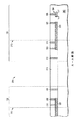
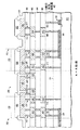
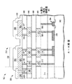
シールリング又は他の連続的なダイ又はウエハ構造と、ダイの上面上の個々のボンドパッドとの間のヒューズめっきバス接続の実施形態を開示する。一実施形態は、シールリング構造の近くのウエハの能動層におけるポリシリコンヒューズを含む。シールリングの接点は、ポリヒューズの第1の端部に直接接続される。最上パッド導体層に電気的に結合された金属/ビアスタックは、ヒューズリンクの第2の端部に接続される。この金属/ビアスタックは、ボンドパッドフットプリントとシールリングとの間に配置されてもよく、ボンドパッドの直下に配置されてもよい。ウエハ上の複数のダイのシールリングが、スクライブストリート又はライン(後でソーイングプロセス中に除去される)に配置される共通の金属トレースに対する電気接続を介してひとまとめにされてもよい。
別の実施形態では、図1〜13に示し、本明細書に記載したように、半導体構造を形成する方法は、半導体基板302の上方にゲート電極304とヒューズ208とを形成する工程と、ゲート電極304とヒューズ208との上方に誘電体層314を形成する工程と、誘電体層314において、シールリング202の第1の部分と、ゲート電極304に対する接点306と、ヒューズ208の第1の端部又は端子に対する第1の接点308と、ヒューズ208の第2の端部又は端子に対する第2の接点310とを形成する工程と、誘電体層314の上方に相互接続層400〜408を形成する工程であって、相互接続層400〜408の形成は、相互接続層400〜408を通じて連続して延びるとともにシールリング202の第1の部分に接続されるシールリング202の第2の部分を形成することを含み、シールリング202は、相互接続層400〜408のうちの1つ以上の相互接続層を通じて第2の接点310に接続される、工程と、相互接続層400〜408の上方に相互接続パッド502を形成する工程であって、相互接続パッド502は相互接続層400〜408を通じて第1の接点308に接続される、工程と、を含む。
さらなる一態様では、ゲート電極304と、ヒューズ208と、相互接続パッド502と、シールリング202とは、第1のダイ102内に存在し、ゲート電極304及びヒューズ208を形成する工程は、第1のダイ102に隣接する第2のダイ102において半導体基板の上方に第2のヒューズ320を形成する工程を含み、誘電体層314は第2のヒューズ320の上方に形成される。シールリング202の第1の部分と、ゲート電極304に対する接点306と、ヒューズ208の第1の端部又は端子に対する第1の接点308と、ヒューズ208の第2の端部又は端子に対する第2の接点310とを形成する工程は、誘電体層314において、第2のシールリング202の第1の部分と、第2のヒューズ320の第1の端部又は端子に対する第1の接点308と、第2のヒューズ320の第2の端部又は端子に対する第2の接点318とを形成する工程を含む。相互接続層400〜408を形成する工程は、複数の相互接続層400〜408を通じて連続して延びるとともに第2のシールリング202の第1の部分に接続される第2のシールリング202の第2の部分を形成する工程であって、第2のシールリング202は、相互接続層400〜408のうちの1つ以上の相互接続層を通じて第2のヒューズ320の第2の端部又は端子に対する第2の接点318に接続される、工程を含む。相互接続パッド502を形成する工程は、相互接続層400〜408の上方に第2の相互接続パッド502を形成する工程を含み、第2の相互接続パッド502は、相互接続層400〜408を通じて第2のヒューズ320の第1の端部又は端子の第1の接点に接続され、第2のヒューズ320と、第2の相互接続パッド502と、第2のシールリング202とは、第2のダイ102内に存在する。
Claims (4)
- 能動回路を包囲するシールリングを備えた複数のダイからなる半導体構造の製造方法において、
半導体基板の上方にゲート電極とヒューズとを形成する工程と、
前記ゲート電極と前記ヒューズとの上方に誘電体層を形成する工程と、
前記誘電体層において、シールリングの第1の部分と、前記ゲート電極に対する接点と、前記ヒューズの第1の端子に対する第1の接点と、前記ヒューズの第2の端子に対する第2の接点とを形成する工程と、
前記誘電体層の上方に複数の相互接続層を形成する工程であって、該工程は、前記複数の相互接続層を通じて連続して延びるとともに前記シールリングの前記第1の部分に接続される前記シールリングの第2の部分を形成する工程を含み、前記シールリングは、前記複数の相互接続層のうちの1つ以上の相互接続層を通じて前記ヒューズの第2の接点に接続される、前記誘電体層の上方に複数の相互接続層を形成する工程と、
前記複数の相互接続層の上方に相互接続パッドを形成する工程であって、該相互接続パッドは前記複数の相互接続層を通じて前記第1の接点に接続される、前記複数の相互接続層の上方に相互接続パッドを形成する工程と、
隣接するダイのそれぞれのシールリングの間に設けられたスクライブストリートで前記隣接するダイを互いから分離すべく、前記複数のダイを個片化する工程と
を備え、個片化した前記ダイを前記シールリングによって汚染イオンから保護する、半導体構造の製造方法。 - 前記シールリングは前記シールリングの第1の部分を含んでなるクラック停止部を有し、前記クラック停止部は前記複数のダイを個片化する工程において生成されるクラックが前記能動回路に入り込むことを防止する、請求項1に記載の半導体構造の製造方法。
- 前記複数の相互接続層の上方に相互接続パッドを形成する工程よりも後に、前記シールリング及び前記複数のヒューズの各々を通じて前記複数の相互接続パッドの各々に電流を提供し、前記複数の相互接続パッドの各々の上に導体層を電気めっきする電気めっき工程をさらに備える、請求項1に記載の半導体構造の製造方法。
- 前記複数のダイを個片化する工程よりも前にそれぞれの前記相互接続パッドに電流を印加して前記半導体構造のウエハ試験を実施する工程をさらに備え、前記電流は前記ヒューズを故障させ、前記能動回路と前記シールリングの間に開回路を形成するために十分である、請求項1に記載の半導体構造の製造方法。
Applications Claiming Priority (2)
| Application Number | Priority Date | Filing Date | Title |
|---|---|---|---|
| US13/189,054 US8349666B1 (en) | 2011-07-22 | 2011-07-22 | Fused buss for plating features on a semiconductor die |
| US13/189,054 | 2011-07-22 |
Publications (3)
| Publication Number | Publication Date |
|---|---|
| JP2013026624A JP2013026624A (ja) | 2013-02-04 |
| JP2013026624A5 JP2013026624A5 (ja) | 2015-09-03 |
| JP6028298B2 true JP6028298B2 (ja) | 2016-11-16 |
Family
ID=46507887
Family Applications (1)
| Application Number | Title | Priority Date | Filing Date |
|---|---|---|---|
| JP2012159145A Active JP6028298B2 (ja) | 2011-07-22 | 2012-07-18 | 半導体ダイ上にフィーチャをめっきするためのヒューズバス |
Country Status (4)
| Country | Link |
|---|---|
| US (1) | US8349666B1 (ja) |
| EP (1) | EP2549532B1 (ja) |
| JP (1) | JP6028298B2 (ja) |
| TW (1) | TWI538152B (ja) |
Cited By (1)
| Publication number | Priority date | Publication date | Assignee | Title |
|---|---|---|---|---|
| JP7009836B2 (ja) | 2017-08-24 | 2022-01-26 | Tdk株式会社 | 部品吸着搬送機 |
Families Citing this family (14)
| Publication number | Priority date | Publication date | Assignee | Title |
|---|---|---|---|---|
| US8519513B2 (en) * | 2012-01-04 | 2013-08-27 | Freescale Semiconductor, Inc. | Semiconductor wafer plating bus |
| JP5968711B2 (ja) * | 2012-07-25 | 2016-08-10 | ルネサスエレクトロニクス株式会社 | 半導体装置及び半導体装置の製造方法 |
| ITMI20121599A1 (it) * | 2012-09-25 | 2014-03-26 | St Microelectronics Srl | Dispositivo elettronico comprendente un transistore vtmos ed un diodo termico integrati |
| US8994148B2 (en) * | 2013-02-19 | 2015-03-31 | Infineon Technologies Ag | Device bond pads over process control monitor structures in a semiconductor die |
| US10424521B2 (en) | 2014-05-13 | 2019-09-24 | Nxp Usa, Inc. | Programmable stitch chaining of die-level interconnects for reliability testing |
| US20150371956A1 (en) * | 2014-06-19 | 2015-12-24 | Globalfoundries Inc. | Crackstops for bulk semiconductor wafers |
| JP6435562B2 (ja) * | 2014-12-02 | 2018-12-12 | ローム株式会社 | 半導体装置および半導体装置の製造方法 |
| US20180337228A1 (en) * | 2017-05-18 | 2018-11-22 | Taiwan Semiconductor Manufacturing Co., Ltd. | Novel seal ring for iii-v compound semiconductor-based devices |
| FR3079342B1 (fr) | 2018-03-21 | 2020-04-17 | Stmicroelectronics (Rousset) Sas | Dispositif fusible integre |
| CN109461717A (zh) * | 2018-10-15 | 2019-03-12 | 上海华虹宏力半导体制造有限公司 | 一种晶圆及其形成方法、等离子体裂片方法 |
| US10978404B2 (en) * | 2019-08-22 | 2021-04-13 | Taiwan Semiconductor Manufacturing Co., Ltd. | Semiconductor structure and method for fabricating semiconductor structure |
| KR20220150158A (ko) * | 2021-05-03 | 2022-11-10 | 에스케이하이닉스 주식회사 | 크랙 전파 가이드를 포함한 반도체 칩을 제조하는 방법 |
| CN113410209B (zh) * | 2021-06-09 | 2023-07-18 | 合肥中感微电子有限公司 | 一种修调电路 |
| JP2023043036A (ja) * | 2021-09-15 | 2023-03-28 | キオクシア株式会社 | 半導体装置 |
Family Cites Families (21)
| Publication number | Priority date | Publication date | Assignee | Title |
|---|---|---|---|---|
| JPS62108543A (ja) * | 1985-11-06 | 1987-05-19 | Hitachi Ltd | 半導体装置の電極形成法 |
| US5384727A (en) * | 1993-11-08 | 1995-01-24 | Advanced Micro Devices, Inc. | Fuse trimming in plastic package devices |
| US6222212B1 (en) | 1994-01-27 | 2001-04-24 | Integrated Device Technology, Inc. | Semiconductor device having programmable interconnect layers |
| US5813881A (en) | 1994-02-08 | 1998-09-29 | Prolinx Labs Corporation | Programmable cable and cable adapter using fuses and antifuses |
| JP3119352B2 (ja) * | 1998-04-15 | 2000-12-18 | 日本電気株式会社 | 半導体装置のメッキ構造体形成方法 |
| US6350633B1 (en) | 2000-08-22 | 2002-02-26 | Charles W. C. Lin | Semiconductor chip assembly with simultaneously electroplated contact terminal and connection joint |
| JP4502173B2 (ja) * | 2003-02-03 | 2010-07-14 | ルネサスエレクトロニクス株式会社 | 半導体装置及びその製造方法 |
| US6911360B2 (en) | 2003-04-29 | 2005-06-28 | Freescale Semiconductor, Inc. | Fuse and method for forming |
| JP2006013229A (ja) * | 2004-06-28 | 2006-01-12 | Toshiba Corp | 半導体装置及びその製造方法 |
| JP4779324B2 (ja) * | 2004-09-01 | 2011-09-28 | セイコーエプソン株式会社 | 半導体装置及び半導体装置の製造方法 |
| US7777338B2 (en) * | 2004-09-13 | 2010-08-17 | Taiwan Semiconductor Manufacturing Co., Ltd. | Seal ring structure for integrated circuit chips |
| US7232711B2 (en) * | 2005-05-24 | 2007-06-19 | International Business Machines Corporation | Method and structure to prevent circuit network charging during fabrication of integrated circuits |
| US8242576B2 (en) * | 2005-07-21 | 2012-08-14 | Taiwan Semiconductor Manufacturing Co., Ltd. | Protection layer for preventing laser damage on semiconductor devices |
| US7575958B2 (en) | 2005-10-11 | 2009-08-18 | Freescale Semiconductor, Inc. | Programmable fuse with silicon germanium |
| US7413980B2 (en) * | 2006-04-25 | 2008-08-19 | Texas Instruments Incorporated | Semiconductor device with improved contact fuse |
| JP2008016707A (ja) * | 2006-07-07 | 2008-01-24 | Matsushita Electric Ind Co Ltd | 半導体装置及びその検査方法 |
| US7586175B2 (en) * | 2006-10-23 | 2009-09-08 | Samsung Electronics Co., Ltd. | Semiconductor wafer having embedded electroplating current paths to provide uniform plating over wafer surface |
| US7948060B2 (en) * | 2008-07-01 | 2011-05-24 | Xmos Limited | Integrated circuit structure |
| US8373254B2 (en) * | 2008-07-29 | 2013-02-12 | Taiwan Semiconductor Manufacturing Company, Ltd. | Structure for reducing integrated circuit corner peeling |
| JP2010153753A (ja) * | 2008-12-26 | 2010-07-08 | Renesas Electronics Corp | 半導体装置 |
| US8865592B2 (en) * | 2009-02-03 | 2014-10-21 | Infineon Technologies Ag | Silicided semiconductor structure and method of forming the same |
-
2011
- 2011-07-22 US US13/189,054 patent/US8349666B1/en active Active
-
2012
- 2012-07-04 EP EP12174973.3A patent/EP2549532B1/en active Active
- 2012-07-18 JP JP2012159145A patent/JP6028298B2/ja active Active
- 2012-07-19 TW TW101126105A patent/TWI538152B/zh active
Cited By (1)
| Publication number | Priority date | Publication date | Assignee | Title |
|---|---|---|---|---|
| JP7009836B2 (ja) | 2017-08-24 | 2022-01-26 | Tdk株式会社 | 部品吸着搬送機 |
Also Published As
| Publication number | Publication date |
|---|---|
| EP2549532A2 (en) | 2013-01-23 |
| TW201320290A (zh) | 2013-05-16 |
| TWI538152B (zh) | 2016-06-11 |
| US20130023091A1 (en) | 2013-01-24 |
| US8349666B1 (en) | 2013-01-08 |
| EP2549532A3 (en) | 2016-12-28 |
| EP2549532B1 (en) | 2020-06-03 |
| JP2013026624A (ja) | 2013-02-04 |
Similar Documents
| Publication | Publication Date | Title |
|---|---|---|
| JP6028298B2 (ja) | 半導体ダイ上にフィーチャをめっきするためのヒューズバス | |
| US8368172B1 (en) | Fused buss for plating features on a semiconductor die | |
| TWI606567B (zh) | 呈奈米尺寸之靜電放電(esd)硬後端結構 | |
| US9048201B2 (en) | Sacrificial wafer probe pads through seal ring for electrical connection to circuit inside an integrated circuit | |
| US7105917B2 (en) | Semiconductor device having a fuse connected to a pad and fabrication method thereof | |
| JP2009246218A (ja) | 半導体装置の製造方法および半導体装置 | |
| TWI654675B (zh) | 半導體裝置結構的形成方法 | |
| CN105720027A (zh) | 半导体器件以及其制造方法 | |
| US9768135B2 (en) | Semiconductor device having conductive bump with improved reliability | |
| US11075155B2 (en) | Package structure and manufacturing method thereof | |
| US11854969B2 (en) | Semiconductor structure and method for forming thereof | |
| US9899333B2 (en) | Method for forming crack-stopping structures | |
| JP2006173476A (ja) | 半導体装置およびその製造方法 | |
| KR20080088653A (ko) | 집적 회로 소자 및 그 제조 방법과, 집적 회로 및 그 제조 방법 | |
| US11495536B2 (en) | Semiconductor structure and method for forming thereof | |
| JP6012688B2 (ja) | 半導体装置 | |
| JP5414219B2 (ja) | ウエハレベルcspにおける絶縁性テスト方法及びこれに用いるtegパターン | |
| TWI793082B (zh) | 晶片封裝體 | |
| JP2012160739A (ja) | 半導体装置 | |
| US9299624B2 (en) | Stacked semiconductor structure and manufacturing method for the same | |
| JP5430848B2 (ja) | 半導体素子、半導体装置、及びそれらの製造方法 | |
| US9263354B2 (en) | Pillar structure having cavities | |
| KR20150033115A (ko) | 반도체 패키지 및 그 제조방법 | |
| JP2010187036A (ja) | 半導体装置およびその製造方法 | |
| JP2013219385A (ja) | 半導体装置 |
Legal Events
| Date | Code | Title | Description |
|---|---|---|---|
| A521 | Request for written amendment filed |
Free format text: JAPANESE INTERMEDIATE CODE: A523 Effective date: 20150721 |
|
| A621 | Written request for application examination |
Free format text: JAPANESE INTERMEDIATE CODE: A621 Effective date: 20150721 |
|
| A977 | Report on retrieval |
Free format text: JAPANESE INTERMEDIATE CODE: A971007 Effective date: 20160608 |
|
| A131 | Notification of reasons for refusal |
Free format text: JAPANESE INTERMEDIATE CODE: A131 Effective date: 20160614 |
|
| A521 | Request for written amendment filed |
Free format text: JAPANESE INTERMEDIATE CODE: A523 Effective date: 20160829 |
|
| TRDD | Decision of grant or rejection written | ||
| A01 | Written decision to grant a patent or to grant a registration (utility model) |
Free format text: JAPANESE INTERMEDIATE CODE: A01 Effective date: 20160920 |
|
| A61 | First payment of annual fees (during grant procedure) |
Free format text: JAPANESE INTERMEDIATE CODE: A61 Effective date: 20160929 |
|
| R150 | Certificate of patent or registration of utility model |
Ref document number: 6028298 Country of ref document: JP Free format text: JAPANESE INTERMEDIATE CODE: R150 |
|
| S533 | Written request for registration of change of name |
Free format text: JAPANESE INTERMEDIATE CODE: R313533 |
|
| R350 | Written notification of registration of transfer |
Free format text: JAPANESE INTERMEDIATE CODE: R350 |
|
| R250 | Receipt of annual fees |
Free format text: JAPANESE INTERMEDIATE CODE: R250 |
|
| R250 | Receipt of annual fees |
Free format text: JAPANESE INTERMEDIATE CODE: R250 |
|
| R250 | Receipt of annual fees |
Free format text: JAPANESE INTERMEDIATE CODE: R250 |
|
| R250 | Receipt of annual fees |
Free format text: JAPANESE INTERMEDIATE CODE: R250 |
|
| R250 | Receipt of annual fees |
Free format text: JAPANESE INTERMEDIATE CODE: R250 |