JP5996215B2 - 光電変換モジュールおよび光伝送ユニット - Google Patents
光電変換モジュールおよび光伝送ユニット Download PDFInfo
- Publication number
- JP5996215B2 JP5996215B2 JP2012042058A JP2012042058A JP5996215B2 JP 5996215 B2 JP5996215 B2 JP 5996215B2 JP 2012042058 A JP2012042058 A JP 2012042058A JP 2012042058 A JP2012042058 A JP 2012042058A JP 5996215 B2 JP5996215 B2 JP 5996215B2
- Authority
- JP
- Japan
- Prior art keywords
- hole
- photoelectric conversion
- substrate
- protrusion
- conversion module
- Prior art date
- Legal status (The legal status is an assumption and is not a legal conclusion. Google has not performed a legal analysis and makes no representation as to the accuracy of the status listed.)
- Expired - Fee Related
Links
Images
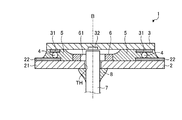


Classifications
-
- G—PHYSICS
- G02—OPTICS
- G02B—OPTICAL ELEMENTS, SYSTEMS OR APPARATUS
- G02B6/00—Light guides; Structural details of arrangements comprising light guides and other optical elements, e.g. couplings
- G02B6/24—Coupling light guides
- G02B6/42—Coupling light guides with opto-electronic elements
- G02B6/4201—Packages, e.g. shape, construction, internal or external details
- G02B6/4219—Mechanical fixtures for holding or positioning the elements relative to each other in the couplings; Alignment methods for the elements, e.g. measuring or observing methods especially used therefor
- G02B6/4236—Fixing or mounting methods of the aligned elements
- G02B6/4245—Mounting of the opto-electronic elements
-
- G—PHYSICS
- G01—MEASURING; TESTING
- G01J—MEASUREMENT OF INTENSITY, VELOCITY, SPECTRAL CONTENT, POLARISATION, PHASE OR PULSE CHARACTERISTICS OF INFRARED, VISIBLE OR ULTRAVIOLET LIGHT; COLORIMETRY; RADIATION PYROMETRY
- G01J1/00—Photometry, e.g. photographic exposure meter
- G01J1/02—Details
- G01J1/0219—Electrical interface; User interface
-
- G—PHYSICS
- G01—MEASURING; TESTING
- G01J—MEASUREMENT OF INTENSITY, VELOCITY, SPECTRAL CONTENT, POLARISATION, PHASE OR PULSE CHARACTERISTICS OF INFRARED, VISIBLE OR ULTRAVIOLET LIGHT; COLORIMETRY; RADIATION PYROMETRY
- G01J1/00—Photometry, e.g. photographic exposure meter
- G01J1/02—Details
- G01J1/04—Optical or mechanical part supplementary adjustable parts
- G01J1/0407—Optical elements not provided otherwise, e.g. manifolds, windows, holograms, gratings
- G01J1/0425—Optical elements not provided otherwise, e.g. manifolds, windows, holograms, gratings using optical fibers
-
- G—PHYSICS
- G02—OPTICS
- G02B—OPTICAL ELEMENTS, SYSTEMS OR APPARATUS
- G02B6/00—Light guides; Structural details of arrangements comprising light guides and other optical elements, e.g. couplings
- G02B6/24—Coupling light guides
- G02B6/42—Coupling light guides with opto-electronic elements
- G02B6/4201—Packages, e.g. shape, construction, internal or external details
- G02B6/4202—Packages, e.g. shape, construction, internal or external details for coupling an active element with fibres without intermediate optical elements, e.g. fibres with plane ends, fibres with shaped ends, bundles
-
- G—PHYSICS
- G02—OPTICS
- G02B—OPTICAL ELEMENTS, SYSTEMS OR APPARATUS
- G02B6/00—Light guides; Structural details of arrangements comprising light guides and other optical elements, e.g. couplings
- G02B6/24—Coupling light guides
- G02B6/42—Coupling light guides with opto-electronic elements
- G02B6/4201—Packages, e.g. shape, construction, internal or external details
- G02B6/4219—Mechanical fixtures for holding or positioning the elements relative to each other in the couplings; Alignment methods for the elements, e.g. measuring or observing methods especially used therefor
- G02B6/4236—Fixing or mounting methods of the aligned elements
- G02B6/4239—Adhesive bonding; Encapsulation with polymer material
-
- G—PHYSICS
- G02—OPTICS
- G02B—OPTICAL ELEMENTS, SYSTEMS OR APPARATUS
- G02B6/00—Light guides; Structural details of arrangements comprising light guides and other optical elements, e.g. couplings
- G02B6/24—Coupling light guides
- G02B6/42—Coupling light guides with opto-electronic elements
- G02B6/4201—Packages, e.g. shape, construction, internal or external details
- G02B6/4251—Sealed packages
- G02B6/4253—Sealed packages by embedding housing components in an adhesive or a polymer material
-
- G—PHYSICS
- G02—OPTICS
- G02B—OPTICAL ELEMENTS, SYSTEMS OR APPARATUS
- G02B6/00—Light guides; Structural details of arrangements comprising light guides and other optical elements, e.g. couplings
- G02B6/24—Coupling light guides
- G02B6/42—Coupling light guides with opto-electronic elements
- G02B6/4201—Packages, e.g. shape, construction, internal or external details
- G02B6/4256—Details of housings
- G02B6/4257—Details of housings having a supporting carrier or a mounting substrate or a mounting plate
-
- H—ELECTRICITY
- H01—ELECTRIC ELEMENTS
- H01S—DEVICES USING THE PROCESS OF LIGHT AMPLIFICATION BY STIMULATED EMISSION OF RADIATION [LASER] TO AMPLIFY OR GENERATE LIGHT; DEVICES USING STIMULATED EMISSION OF ELECTROMAGNETIC RADIATION IN WAVE RANGES OTHER THAN OPTICAL
- H01S5/00—Semiconductor lasers
- H01S5/02—Structural details or components not essential to laser action
- H01S5/022—Mountings; Housings
- H01S5/0225—Out-coupling of light
- H01S5/02251—Out-coupling of light using optical fibres
-
- H—ELECTRICITY
- H01—ELECTRIC ELEMENTS
- H01S—DEVICES USING THE PROCESS OF LIGHT AMPLIFICATION BY STIMULATED EMISSION OF RADIATION [LASER] TO AMPLIFY OR GENERATE LIGHT; DEVICES USING STIMULATED EMISSION OF ELECTROMAGNETIC RADIATION IN WAVE RANGES OTHER THAN OPTICAL
- H01S5/00—Semiconductor lasers
- H01S5/02—Structural details or components not essential to laser action
- H01S5/022—Mountings; Housings
- H01S5/0233—Mounting configuration of laser chips
- H01S5/0234—Up-side down mountings, e.g. Flip-chip, epi-side down mountings or junction down mountings
-
- H—ELECTRICITY
- H10—SEMICONDUCTOR DEVICES; ELECTRIC SOLID-STATE DEVICES NOT OTHERWISE PROVIDED FOR
- H10W—GENERIC PACKAGES, INTERCONNECTIONS, CONNECTORS OR OTHER CONSTRUCTIONAL DETAILS OF DEVICES COVERED BY CLASS H10
- H10W90/00—Package configurations
- H10W90/20—Configurations of stacked chips
- H10W90/293—Configurations of stacked chips characterised by non-galvanic coupling between the chips, e.g. capacitive coupling
-
- H—ELECTRICITY
- H01—ELECTRIC ELEMENTS
- H01S—DEVICES USING THE PROCESS OF LIGHT AMPLIFICATION BY STIMULATED EMISSION OF RADIATION [LASER] TO AMPLIFY OR GENERATE LIGHT; DEVICES USING STIMULATED EMISSION OF ELECTROMAGNETIC RADIATION IN WAVE RANGES OTHER THAN OPTICAL
- H01S5/00—Semiconductor lasers
- H01S5/02—Structural details or components not essential to laser action
- H01S5/022—Mountings; Housings
- H01S5/02218—Material of the housings; Filling of the housings
- H01S5/02234—Resin-filled housings; the housings being made of resin
-
- H—ELECTRICITY
- H01—ELECTRIC ELEMENTS
- H01S—DEVICES USING THE PROCESS OF LIGHT AMPLIFICATION BY STIMULATED EMISSION OF RADIATION [LASER] TO AMPLIFY OR GENERATE LIGHT; DEVICES USING STIMULATED EMISSION OF ELECTROMAGNETIC RADIATION IN WAVE RANGES OTHER THAN OPTICAL
- H01S5/00—Semiconductor lasers
- H01S5/02—Structural details or components not essential to laser action
- H01S5/022—Mountings; Housings
- H01S5/0235—Method for mounting laser chips
- H01S5/02355—Fixing laser chips on mounts
- H01S5/0237—Fixing laser chips on mounts by soldering
-
- H—ELECTRICITY
- H01—ELECTRIC ELEMENTS
- H01S—DEVICES USING THE PROCESS OF LIGHT AMPLIFICATION BY STIMULATED EMISSION OF RADIATION [LASER] TO AMPLIFY OR GENERATE LIGHT; DEVICES USING STIMULATED EMISSION OF ELECTROMAGNETIC RADIATION IN WAVE RANGES OTHER THAN OPTICAL
- H01S5/00—Semiconductor lasers
- H01S5/10—Construction or shape of the optical resonator, e.g. extended or external cavity, coupled cavities, bent-guide, varying width, thickness or composition of the active region
- H01S5/18—Surface-emitting [SE] lasers, e.g. having both horizontal and vertical cavities
- H01S5/183—Surface-emitting [SE] lasers, e.g. having both horizontal and vertical cavities having only vertical cavities, e.g. vertical cavity surface-emitting lasers [VCSEL]
-
- H—ELECTRICITY
- H10—SEMICONDUCTOR DEVICES; ELECTRIC SOLID-STATE DEVICES NOT OTHERWISE PROVIDED FOR
- H10W—GENERIC PACKAGES, INTERCONNECTIONS, CONNECTORS OR OTHER CONSTRUCTIONAL DETAILS OF DEVICES COVERED BY CLASS H10
- H10W70/00—Package substrates; Interposers; Redistribution layers [RDL]
- H10W70/60—Insulating or insulated package substrates; Interposers; Redistribution layers
- H10W70/67—Insulating or insulated package substrates; Interposers; Redistribution layers characterised by their insulating layers or insulating parts
- H10W70/68—Shapes or dispositions thereof
- H10W70/681—Shapes or dispositions thereof comprising holes not having chips therein, e.g. for outgassing, underfilling or bond wire passage
-
- H—ELECTRICITY
- H10—SEMICONDUCTOR DEVICES; ELECTRIC SOLID-STATE DEVICES NOT OTHERWISE PROVIDED FOR
- H10W—GENERIC PACKAGES, INTERCONNECTIONS, CONNECTORS OR OTHER CONSTRUCTIONAL DETAILS OF DEVICES COVERED BY CLASS H10
- H10W90/00—Package configurations
- H10W90/701—Package configurations characterised by the relative positions of pads or connectors relative to package parts
- H10W90/721—Package configurations characterised by the relative positions of pads or connectors relative to package parts of bump connectors
- H10W90/724—Package configurations characterised by the relative positions of pads or connectors relative to package parts of bump connectors between a chip and a stacked insulating package substrate, interposer or RDL
Landscapes
- Physics & Mathematics (AREA)
- General Physics & Mathematics (AREA)
- Optics & Photonics (AREA)
- Condensed Matter Physics & Semiconductors (AREA)
- Electromagnetism (AREA)
- Spectroscopy & Molecular Physics (AREA)
- Engineering & Computer Science (AREA)
- Human Computer Interaction (AREA)
- Optical Couplings Of Light Guides (AREA)
- Semiconductor Lasers (AREA)
Priority Applications (3)
| Application Number | Priority Date | Filing Date | Title |
|---|---|---|---|
| JP2012042058A JP5996215B2 (ja) | 2012-02-28 | 2012-02-28 | 光電変換モジュールおよび光伝送ユニット |
| PCT/JP2013/052391 WO2013129026A1 (ja) | 2012-02-28 | 2013-02-01 | 光電変換モジュールおよび光伝送ユニット |
| US14/466,246 US9625664B2 (en) | 2012-02-28 | 2014-08-22 | Photoelectric conversion module and optical transmission unit |
Applications Claiming Priority (1)
| Application Number | Priority Date | Filing Date | Title |
|---|---|---|---|
| JP2012042058A JP5996215B2 (ja) | 2012-02-28 | 2012-02-28 | 光電変換モジュールおよび光伝送ユニット |
Publications (3)
| Publication Number | Publication Date |
|---|---|
| JP2013178378A JP2013178378A (ja) | 2013-09-09 |
| JP2013178378A5 JP2013178378A5 (OSRAM) | 2015-04-02 |
| JP5996215B2 true JP5996215B2 (ja) | 2016-09-21 |
Family
ID=49082230
Family Applications (1)
| Application Number | Title | Priority Date | Filing Date |
|---|---|---|---|
| JP2012042058A Expired - Fee Related JP5996215B2 (ja) | 2012-02-28 | 2012-02-28 | 光電変換モジュールおよび光伝送ユニット |
Country Status (3)
| Country | Link |
|---|---|
| US (1) | US9625664B2 (OSRAM) |
| JP (1) | JP5996215B2 (OSRAM) |
| WO (1) | WO2013129026A1 (OSRAM) |
Families Citing this family (6)
| Publication number | Priority date | Publication date | Assignee | Title |
|---|---|---|---|---|
| JP6230388B2 (ja) * | 2013-11-28 | 2017-11-15 | オリンパス株式会社 | 内視鏡 |
| US10025044B1 (en) * | 2017-01-17 | 2018-07-17 | International Business Machines Corporation | Optical structure |
| JP6641330B2 (ja) * | 2017-08-31 | 2020-02-05 | 株式会社フジクラ | 撮像モジュール付きカテーテル |
| DE102017123798B4 (de) * | 2017-10-12 | 2022-03-03 | OSRAM Opto Semiconductors Gesellschaft mit beschränkter Haftung | Halbleiterlaser und Herstellungsverfahren für optoelektronische Halbleiterbauteile |
| US20230054960A1 (en) * | 2020-02-04 | 2023-02-23 | Panasonic Intellectual Property Management Co., Ltd. | Side-filling resin composition, semiconductor device, and method for removing side-filling member |
| US20230085957A1 (en) * | 2021-09-22 | 2023-03-23 | Apple Inc. | Integrated optical transceiver |
Family Cites Families (18)
| Publication number | Priority date | Publication date | Assignee | Title |
|---|---|---|---|---|
| GB8912376D0 (en) | 1989-05-30 | 1989-07-12 | Hughes Microelectronics Ltd | Photoelectric components |
| FR2672697B1 (fr) * | 1991-02-08 | 1994-06-03 | Alcatel Nv | Dispositif optoelectronique monte sur substrat et connecte par fibre optique, et son procede de fabrication. |
| JP3166564B2 (ja) * | 1995-06-27 | 2001-05-14 | 松下電器産業株式会社 | 半導体レーザ実装体およびその製造方法 |
| JPH11121653A (ja) * | 1997-07-31 | 1999-04-30 | Fuji Film Microdevices Co Ltd | 半導体装置とその製造方法 |
| JP2001059923A (ja) * | 1999-06-16 | 2001-03-06 | Seiko Epson Corp | 光モジュール及びその製造方法、半導体装置並びに光伝達装置 |
| JP2001250889A (ja) * | 2000-03-06 | 2001-09-14 | Matsushita Electric Ind Co Ltd | 光素子の実装構造体およびその製造方法 |
| JP4113722B2 (ja) * | 2001-04-18 | 2008-07-09 | 松下電器産業株式会社 | 半導体モジュールとその製造方法 |
| JP4062403B2 (ja) * | 2001-11-06 | 2008-03-19 | セイコーエプソン株式会社 | 光モジュールの製造方法 |
| JP2003209332A (ja) * | 2002-01-11 | 2003-07-25 | Fujikura Ltd | プリント配線基板、プリント配線基板の製造方法、及び実装基板 |
| JP2004258528A (ja) * | 2003-02-27 | 2004-09-16 | Seiko Epson Corp | 光通信モジュールの製造方法および電子機器 |
| JP2004317627A (ja) * | 2003-04-14 | 2004-11-11 | Fujikura Ltd | マウント、光モジュールおよび送受信モジュール |
| JP2005286284A (ja) * | 2004-02-03 | 2005-10-13 | Sony Chem Corp | 機能素子実装モジュール並びに光機能素子実装モジュール及びその製造方法 |
| JP2005268567A (ja) * | 2004-03-19 | 2005-09-29 | Matsushita Electric Ind Co Ltd | 基板およびその製造方法 |
| JP4184371B2 (ja) | 2005-10-03 | 2008-11-19 | 日本テキサス・インスツルメンツ株式会社 | 半導体チップ、半導体装置およびそれらの製造方法 |
| JP2008182026A (ja) * | 2007-01-24 | 2008-08-07 | Sony Chemical & Information Device Corp | 機能素子実装モジュールの製造方法 |
| JP2009047937A (ja) | 2007-08-20 | 2009-03-05 | Sony Corp | 光送信/光受信モジュール及び光モジュールの製造方法並びに光通信モジュール |
| JP2009251224A (ja) | 2008-04-04 | 2009-10-29 | Sumitomo Electric Ind Ltd | 光モジュール及びその組立方法 |
| JP5809866B2 (ja) | 2011-07-21 | 2015-11-11 | オリンパス株式会社 | 光素子モジュール、光伝送モジュール、および光伝送モジュールの製造方法 |
-
2012
- 2012-02-28 JP JP2012042058A patent/JP5996215B2/ja not_active Expired - Fee Related
-
2013
- 2013-02-01 WO PCT/JP2013/052391 patent/WO2013129026A1/ja not_active Ceased
-
2014
- 2014-08-22 US US14/466,246 patent/US9625664B2/en not_active Expired - Fee Related
Also Published As
| Publication number | Publication date |
|---|---|
| WO2013129026A1 (ja) | 2013-09-06 |
| US20140361153A1 (en) | 2014-12-11 |
| US9625664B2 (en) | 2017-04-18 |
| JP2013178378A (ja) | 2013-09-09 |
Similar Documents
| Publication | Publication Date | Title |
|---|---|---|
| JP5809866B2 (ja) | 光素子モジュール、光伝送モジュール、および光伝送モジュールの製造方法 | |
| CN101131983B (zh) | 连接体和光发送接收模块 | |
| JP2013178378A (ja) | 光電変換モジュールおよび光伝送ユニット | |
| JP5757852B2 (ja) | 撮像モジュールおよび撮像ユニット | |
| JP5421863B2 (ja) | 半導体パッケージの製造方法 | |
| US9615464B2 (en) | Method of mounting semiconductor element, and semiconductor device | |
| JP2017108064A (ja) | 光モジュール | |
| JP4768384B2 (ja) | 光伝送路保持部材及び光モジュール | |
| JP4406447B2 (ja) | 光モジュールおよびその製造方法 | |
| JP5706254B2 (ja) | 半導体装置 | |
| JP5078021B2 (ja) | 光導波路モジュール、光導波路モジュールの製造方法 | |
| CN106104340A (zh) | 光传送模块和光传送模块的制造方法 | |
| JP2012018231A (ja) | 光伝送路保持部材と光モジュール | |
| US20050013557A1 (en) | Optical packages and methods for controlling a standoff height in optical packages | |
| JP2009283918A (ja) | 配線基板と配線基板の接続方法 | |
| TW202121626A (zh) | 接合結構以及製造接合結構之方法 | |
| JP2018137305A (ja) | 電子装置及び電子装置の製造方法 | |
| JP2013125768A (ja) | はんだ接合デバイス及び受信モジュール | |
| JP6089732B2 (ja) | 導電性部材の接続構造、導電性部材の接続方法、及び光モジュール | |
| JP4960519B2 (ja) | 光伝送路保持部材及び光モジュール | |
| JP2004317632A (ja) | 光モジュール用マウント部材、光モジュール、光モジュールの製造方法 | |
| JP2010021471A (ja) | 半導体装置および半導体装置の製造方法 | |
| JPWO2017141369A1 (ja) | 光伝送モジュールおよび内視鏡 | |
| WO2021020530A1 (ja) | 電子素子搭載用パッケージ及び電子装置 | |
| JP3726718B2 (ja) | 半導体装置 |
Legal Events
| Date | Code | Title | Description |
|---|---|---|---|
| A521 | Request for written amendment filed |
Free format text: JAPANESE INTERMEDIATE CODE: A523 Effective date: 20150210 |
|
| A621 | Written request for application examination |
Free format text: JAPANESE INTERMEDIATE CODE: A621 Effective date: 20150210 |
|
| A131 | Notification of reasons for refusal |
Free format text: JAPANESE INTERMEDIATE CODE: A131 Effective date: 20160119 |
|
| A521 | Request for written amendment filed |
Free format text: JAPANESE INTERMEDIATE CODE: A523 Effective date: 20160311 |
|
| TRDD | Decision of grant or rejection written | ||
| A01 | Written decision to grant a patent or to grant a registration (utility model) |
Free format text: JAPANESE INTERMEDIATE CODE: A01 Effective date: 20160802 |
|
| A61 | First payment of annual fees (during grant procedure) |
Free format text: JAPANESE INTERMEDIATE CODE: A61 Effective date: 20160824 |
|
| R151 | Written notification of patent or utility model registration |
Ref document number: 5996215 Country of ref document: JP Free format text: JAPANESE INTERMEDIATE CODE: R151 |
|
| R250 | Receipt of annual fees |
Free format text: JAPANESE INTERMEDIATE CODE: R250 |
|
| R250 | Receipt of annual fees |
Free format text: JAPANESE INTERMEDIATE CODE: R250 |
|
| R250 | Receipt of annual fees |
Free format text: JAPANESE INTERMEDIATE CODE: R250 |
|
| R250 | Receipt of annual fees |
Free format text: JAPANESE INTERMEDIATE CODE: R250 |
|
| LAPS | Cancellation because of no payment of annual fees |