JP5757852B2 - 撮像モジュールおよび撮像ユニット - Google Patents
撮像モジュールおよび撮像ユニット Download PDFInfo
- Publication number
- JP5757852B2 JP5757852B2 JP2011266073A JP2011266073A JP5757852B2 JP 5757852 B2 JP5757852 B2 JP 5757852B2 JP 2011266073 A JP2011266073 A JP 2011266073A JP 2011266073 A JP2011266073 A JP 2011266073A JP 5757852 B2 JP5757852 B2 JP 5757852B2
- Authority
- JP
- Japan
- Prior art keywords
- electrode
- chip
- cable
- imaging
- disposed
- Prior art date
- Legal status (The legal status is an assumption and is not a legal conclusion. Google has not performed a legal analysis and makes no representation as to the accuracy of the status listed.)
- Active
Links
- 238000003384 imaging method Methods 0.000 title claims description 104
- 230000002093 peripheral effect Effects 0.000 claims description 7
- 230000003287 optical effect Effects 0.000 claims description 5
- 230000004048 modification Effects 0.000 description 18
- 238000012986 modification Methods 0.000 description 18
- 238000001444 catalytic combustion detection Methods 0.000 description 16
- 239000011347 resin Substances 0.000 description 12
- 229920005989 resin Polymers 0.000 description 12
- 238000007789 sealing Methods 0.000 description 10
- 238000005304 joining Methods 0.000 description 8
- 238000004519 manufacturing process Methods 0.000 description 8
- 239000006059 cover glass Substances 0.000 description 7
- XUIMIQQOPSSXEZ-UHFFFAOYSA-N Silicon Chemical compound [Si] XUIMIQQOPSSXEZ-UHFFFAOYSA-N 0.000 description 6
- 229910052710 silicon Inorganic materials 0.000 description 6
- 239000010703 silicon Substances 0.000 description 6
- 239000012790 adhesive layer Substances 0.000 description 5
- 238000010438 heat treatment Methods 0.000 description 4
- 238000000034 method Methods 0.000 description 4
- 230000000149 penetrating effect Effects 0.000 description 3
- 229910000679 solder Inorganic materials 0.000 description 3
- 230000015572 biosynthetic process Effects 0.000 description 2
- 239000004020 conductor Substances 0.000 description 2
- 230000000694 effects Effects 0.000 description 2
- 239000011521 glass Substances 0.000 description 2
- 230000003014 reinforcing effect Effects 0.000 description 2
- 239000004065 semiconductor Substances 0.000 description 2
- WGTYBPLFGIVFAS-UHFFFAOYSA-M tetramethylammonium hydroxide Chemical compound [OH-].C[N+](C)(C)C WGTYBPLFGIVFAS-UHFFFAOYSA-M 0.000 description 2
- 239000004925 Acrylic resin Substances 0.000 description 1
- 229920000178 Acrylic resin Polymers 0.000 description 1
- 239000012670 alkaline solution Substances 0.000 description 1
- 230000005540 biological transmission Effects 0.000 description 1
- 239000003990 capacitor Substances 0.000 description 1
- 238000005520 cutting process Methods 0.000 description 1
- 238000010586 diagram Methods 0.000 description 1
- 238000001312 dry etching Methods 0.000 description 1
- 238000005516 engineering process Methods 0.000 description 1
- 239000003822 epoxy resin Substances 0.000 description 1
- 238000005530 etching Methods 0.000 description 1
- PCHJSUWPFVWCPO-UHFFFAOYSA-N gold Chemical compound [Au] PCHJSUWPFVWCPO-UHFFFAOYSA-N 0.000 description 1
- 229910052737 gold Inorganic materials 0.000 description 1
- 239000010931 gold Substances 0.000 description 1
- 238000009434 installation Methods 0.000 description 1
- 238000004093 laser heating Methods 0.000 description 1
- 239000010410 layer Substances 0.000 description 1
- 238000002844 melting Methods 0.000 description 1
- 230000008018 melting Effects 0.000 description 1
- 239000005011 phenolic resin Substances 0.000 description 1
- 229920002120 photoresistant polymer Polymers 0.000 description 1
- 238000007747 plating Methods 0.000 description 1
- 229920000647 polyepoxide Polymers 0.000 description 1
- 238000003825 pressing Methods 0.000 description 1
- 229920002050 silicone resin Polymers 0.000 description 1
- 230000008646 thermal stress Effects 0.000 description 1
- 238000001039 wet etching Methods 0.000 description 1
Images


Classifications
-
- H—ELECTRICITY
- H01—ELECTRIC ELEMENTS
- H01L—SEMICONDUCTOR DEVICES NOT COVERED BY CLASS H10
- H01L31/00—Semiconductor devices sensitive to infrared radiation, light, electromagnetic radiation of shorter wavelength or corpuscular radiation and specially adapted either for the conversion of the energy of such radiation into electrical energy or for the control of electrical energy by such radiation; Processes or apparatus specially adapted for the manufacture or treatment thereof or of parts thereof; Details thereof
- H01L31/02—Details
- H01L31/02002—Arrangements for conducting electric current to or from the device in operations
- H01L31/02005—Arrangements for conducting electric current to or from the device in operations for device characterised by at least one potential jump barrier or surface barrier
-
- G—PHYSICS
- G02—OPTICS
- G02B—OPTICAL ELEMENTS, SYSTEMS OR APPARATUS
- G02B7/00—Mountings, adjusting means, or light-tight connections, for optical elements
- G02B7/02—Mountings, adjusting means, or light-tight connections, for optical elements for lenses
-
- H—ELECTRICITY
- H01—ELECTRIC ELEMENTS
- H01L—SEMICONDUCTOR DEVICES NOT COVERED BY CLASS H10
- H01L27/00—Devices consisting of a plurality of semiconductor or other solid-state components formed in or on a common substrate
- H01L27/14—Devices consisting of a plurality of semiconductor or other solid-state components formed in or on a common substrate including semiconductor components sensitive to infrared radiation, light, electromagnetic radiation of shorter wavelength or corpuscular radiation and specially adapted either for the conversion of the energy of such radiation into electrical energy or for the control of electrical energy by such radiation
- H01L27/144—Devices controlled by radiation
- H01L27/146—Imager structures
- H01L27/14601—Structural or functional details thereof
- H01L27/14618—Containers
-
- H—ELECTRICITY
- H01—ELECTRIC ELEMENTS
- H01L—SEMICONDUCTOR DEVICES NOT COVERED BY CLASS H10
- H01L27/00—Devices consisting of a plurality of semiconductor or other solid-state components formed in or on a common substrate
- H01L27/14—Devices consisting of a plurality of semiconductor or other solid-state components formed in or on a common substrate including semiconductor components sensitive to infrared radiation, light, electromagnetic radiation of shorter wavelength or corpuscular radiation and specially adapted either for the conversion of the energy of such radiation into electrical energy or for the control of electrical energy by such radiation
- H01L27/144—Devices controlled by radiation
- H01L27/146—Imager structures
- H01L27/14683—Processes or apparatus peculiar to the manufacture or treatment of these devices or parts thereof
- H01L27/1469—Assemblies, i.e. hybrid integration
-
- H—ELECTRICITY
- H04—ELECTRIC COMMUNICATION TECHNIQUE
- H04N—PICTORIAL COMMUNICATION, e.g. TELEVISION
- H04N23/00—Cameras or camera modules comprising electronic image sensors; Control thereof
- H04N23/50—Constructional details
- H04N23/54—Mounting of pick-up tubes, electronic image sensors, deviation or focusing coils
-
- H—ELECTRICITY
- H04—ELECTRIC COMMUNICATION TECHNIQUE
- H04N—PICTORIAL COMMUNICATION, e.g. TELEVISION
- H04N23/00—Cameras or camera modules comprising electronic image sensors; Control thereof
- H04N23/57—Mechanical or electrical details of cameras or camera modules specially adapted for being embedded in other devices
-
- H—ELECTRICITY
- H01—ELECTRIC ELEMENTS
- H01L—SEMICONDUCTOR DEVICES NOT COVERED BY CLASS H10
- H01L2924/00—Indexing scheme for arrangements or methods for connecting or disconnecting semiconductor or solid-state bodies as covered by H01L24/00
- H01L2924/0001—Technical content checked by a classifier
- H01L2924/0002—Not covered by any one of groups H01L24/00, H01L24/00 and H01L2224/00
Description
図2〜図4を用いて、本発明の実施形態の撮像モジュール1の構造について説明する。なお図は、いずれも説明のための模式図であり、縦横の寸法比等は実際とは異なっている。また一部の構成要素の図示を省略することがある。
撮像モジュール1は、配線板30の第2の主面30SBにケーブル40を接合した後に、CSPタイプの撮像チップ50を配線板30の第1の主面30SAすることで製造される。
図5に示すように、シリコンウエハ20Wのおもて面に公知の半導体技術を用いて複数のCCD21および複数の信号処理回路(不図示)が形成される。なお、CCD21上に、マイクロレンズおよびカラーフィルタを配設してもよい。また、固体撮像素子としてはCOMSイメージセンサ等でもよい。
シリコンウエハ20Wのおもて面、すなわち、CCD21形成面に、接着層19Wを介して透明なガラスウエハ10Wが接合されることで接合ウエハ50Wが作製される。CCD21の少なくとも有効撮像素子形成領域の上の接着層19Wには開口が形成されている。このため、シリコンウエハ20WのCCD21形成領域と、ガラスウエハ10Wとの間には、空洞部が形成される。なお、撮像モジュールの仕様によっては、空洞部を形成する必要がない場合もある。
接合ウエハ50W(シリコンウエハ20W)の裏面にフォトレジストを用いて、CCD電極パッド22と対向する位置に開口のあるエッチングマスクが配設される。そして、裏面側からのICP−RIE等のドライエッチングを用いて、シリコンウエハ20Wを貫通しCCD電極パッド22の裏面に到達する貫通孔が形成される。貫通孔の形成には、例えば、KOHまたはTMAH等のアルカリ溶液を用いたウエットエッチングを用いてもよい。
接合ウエハ50Wが、図5に示す破線に沿ってブレードダイシング法により切断/個片化されることにより、一括して複数の撮像チップ50が作製される。
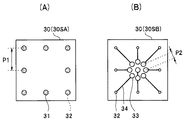
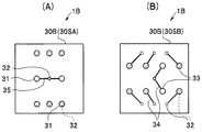
別途、例えば、両面配線基板を用いて、配線板30が作製される。配線板30は、第1の主面30SAの外周部に複数のチップ電極31を有する。それぞれのチップ電極31の位置は、撮像チップ50の対応する外部電極24の位置と、一致するように設定されている。チップ電極31の直下には第2の主面30SBに到達する貫通配線32が形成されている。一方、配線板30は、第2の主面30SBの中央部に複数のケーブル電極33を有する。表面配線34を介して貫通配線32と接続されたケーブル電極33は、ケーブル40の対応する導線42の位置と、一致するように設定されている。なお、すでに説明したように、撮像モジュール1の細径化のために、配線板30の外寸は、撮像チップ50の外寸よりも小さい。
配線板30のケーブル電極33とケーブル40の導線42とが、接合される。接合には、接合部に外部からエネルギーを印加する必要がある。例えば、はんだ接合の場合には、熱エネルギーが局所的に印加された接合箇所が、はんだ融点以上に加熱される。局所加熱には、ヒーター加熱、レーザー加熱またはランプ加熱等を用い、必要に応じて圧力を加えながら加熱してもよい。なお、熱エネルギー印加に換えて、異なるエネルギーの印加、例えば超音波エネルギー等の印加により接合してもよい。
ケーブル40が接合された配線板30のチップ電極31に、撮像チップ50の外部電極24が接合される。ケーブル電極33とケーブル40との接合と同様に、この接合にも接合部にエネルギーの印加が必要である。
次に、実施形態の変形例の撮像モジュール1A〜1Eについて説明する。変形例の撮像モジュール1A〜1Eは、実施形態の撮像モジュール1と類似しているので、同じ構成要素には同じ符号を付し説明は省略する。
図8(A)に示すように、変形例1の撮像モジュール1Aでは、配線板30Aの第1の主面30SAの中央部にチップ電極31が配設され、表面配線35を介してチップ電極31と離れた位置にある貫通配線32と接続されている。そして、図8(B)に示すように、配線板30Aの第2の主面30SBの周辺部に形成された貫通配線32の直上にケーブル電極33が配設されている。
図9(A)に示すように、変形例2の撮像モジュール1Bでは、配線板30Bの第1の主面30SAの中央部および周辺部にチップ電極31が配設されている。一部のチップ電極31は表面配線35を介して貫通配線32と接続されており、一部のチップ電極31は直下の貫通配線32と接続されている。そして、図9(B)に示すように、配線板30Bの第2の主面30SBの中央部および周辺部にケーブル電極33が配設されている。一部のケーブル電極33は、貫通配線32の直上に配設されており、一部のケーブル電極33は、表面配線34を介して貫通配線32と離れた位置に配設されている。また一部の貫通配線32は表面配線34、35を介してケーブル電極33とチップ電極31とを接続している。
図10(A)に示すように、変形例3の撮像モジュール1Cでは、配線板30Cの第1の主面30SAの中央から偏芯した領域に複数のチップ電極31が配設されている。そして、撮像モジュール1Bと同様に、第1の主面30SAに表面配線35が配設されており、第2の主面30SBにも表面配線34が配設されており、ケーブル電極33は、チップ電極31の配設領域と対向していない領域に配設されている。なお、第1の主面30SAのチップ電極31Cは、接合のバランスを確保するためのダミー電極である。
図11に示すように、変形例4の撮像モジュール1Dでは、ケーブル40の複数の導線42の端部が、配線板30の複数のケーブル電極33の配列にあわせて再配列され、ブロック部材43により一体化されている。
図12に示すように、変形例5の撮像モジュール1Eでは、ケーブル40の複数の導線42の端部が、配線板30の複数のケーブル電極33の配列にあわせて折り曲げられている。そして、ケーブル電極33と導線42とは、はんだ付けされている。
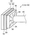
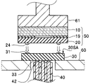
図13に示すように、本発明の第2実施形態の撮像ユニット2は、すでに説明した撮像モジュール1と、撮像素子チップの受光面に被写体像を結像する光学部材と、を具備する。すなわち、撮像ユニット2は、レンズユニット62(光学レンズおよびそれを保持するレンズバレル)とそれを保持するレンズユニットホルダ63とが、撮像モジュール1とともにシールド枠64の内側に収容されており、ケーブル40は充填樹脂65により封止されている。撮像モジュール1を具備する撮像ユニット2は、接続信頼性が高く、細径であるために、電子内視鏡の先端部に配設するのに適している。なお、撮像モジュール1に替えて撮像モジュール1A〜1Eを具備している撮像ユニットも、撮像ユニット2と同様の効果を有する。
2…撮像ユニット
10…カバーガラス
19…接着層
20…撮像素子チップ
21…CCD
22…CCD電極
23…貫通配線
24…外部電極
29…封止樹脂
30…配線板
31…チップ電極
32…貫通配線
33…ケーブル電極
34、35…表面配線
36…電子部品
40…ケーブル
42…導線
49…封止樹脂
50…撮像チップ
50W…接合ウエハ
60…ステージ
61…コレット
62…レンズユニット
63…レンズユニットホルダ
64…シールド枠
65…充填樹脂
Claims (5)
- 第1の主面にチップ電極が配設されており、第2の主面に貫通配線を介して前記チップ電極と接続されているケーブル電極が配設されている配線板と、
前記チップ電極と接合された外部電極を有する撮像素子チップと、
前記ケーブル電極と接合された導線を有するケーブルと、を具備する撮像モジュールであって、
全ての前記ケーブル電極が前記チップ電極の配設領域と対向していない領域に配設されていることを特徴とする。 - 前記チップ電極が、前記第1の主面の外周部に配設されており、
前記ケーブル電極が、前記第2の主面の中央部に配設されていることを特徴とする請求項1に記載の撮像モジュール。 - 前記チップ電極が、前記第1の主面の中央部に配設されており、
前記ケーブル電極が、前記第2の主面の外周部に配設されていることを特徴とする請求項1に記載の撮像モジュール。 - 前記配線板の、前記第2の主面の前記チップ電極の配設領域と対向していない領域に電子部品が表面実装されていることを特徴とする請求項1に記載の撮像モジュール。
- 請求項1から請求項4のいずれか1項に記載の撮像モジュールと、前記撮像素子チップの受光面に被写体像を結像する光学部材と、を具備することを特徴とする撮像ユニット。
Priority Applications (4)
| Application Number | Priority Date | Filing Date | Title |
|---|---|---|---|
| JP2011266073A JP5757852B2 (ja) | 2011-12-05 | 2011-12-05 | 撮像モジュールおよび撮像ユニット |
| EP12854656.1A EP2790218A4 (en) | 2011-12-05 | 2012-09-07 | IMAGING MODULE AND IMAGING UNIT |
| PCT/JP2012/072882 WO2013084553A1 (ja) | 2011-12-05 | 2012-09-07 | 撮像モジュールおよび撮像ユニット |
| US14/291,178 US9455358B2 (en) | 2011-12-05 | 2014-05-30 | Image pickup module and image pickup unit |
Applications Claiming Priority (1)
| Application Number | Priority Date | Filing Date | Title |
|---|---|---|---|
| JP2011266073A JP5757852B2 (ja) | 2011-12-05 | 2011-12-05 | 撮像モジュールおよび撮像ユニット |
Publications (3)
| Publication Number | Publication Date |
|---|---|
| JP2013118337A JP2013118337A (ja) | 2013-06-13 |
| JP2013118337A5 JP2013118337A5 (ja) | 2015-01-15 |
| JP5757852B2 true JP5757852B2 (ja) | 2015-08-05 |
Family
ID=48573937
Family Applications (1)
| Application Number | Title | Priority Date | Filing Date |
|---|---|---|---|
| JP2011266073A Active JP5757852B2 (ja) | 2011-12-05 | 2011-12-05 | 撮像モジュールおよび撮像ユニット |
Country Status (4)
| Country | Link |
|---|---|
| US (1) | US9455358B2 (ja) |
| EP (1) | EP2790218A4 (ja) |
| JP (1) | JP5757852B2 (ja) |
| WO (1) | WO2013084553A1 (ja) |
Families Citing this family (13)
| Publication number | Priority date | Publication date | Assignee | Title |
|---|---|---|---|---|
| JP6344935B2 (ja) * | 2014-03-13 | 2018-06-20 | Hoya株式会社 | 半導体装置及び内視鏡 |
| JPWO2015141802A1 (ja) * | 2014-03-20 | 2017-04-13 | オリンパス株式会社 | 実装構造体の製造方法、実装用治具、実装構造体の製造装置、撮像装置および内視鏡装置 |
| JP6515431B2 (ja) * | 2015-03-31 | 2019-05-22 | 国立大学法人東北大学 | 挿入器具および挿入器具の製造方法 |
| CN107431767A (zh) | 2015-04-17 | 2017-12-01 | 奥林巴斯株式会社 | 摄像装置 |
| CN107613838A (zh) * | 2015-05-29 | 2018-01-19 | 奥林巴斯株式会社 | 摄像装置、内窥镜系统以及摄像装置的制造方法 |
| US10122953B2 (en) | 2015-11-30 | 2018-11-06 | Fujikura Ltd. | Imaging module |
| JP2019047300A (ja) | 2017-08-31 | 2019-03-22 | 株式会社フジクラ | 撮像モジュール及びハーネスユニット |
| TWI646939B (zh) * | 2017-11-10 | 2019-01-11 | 沅聖科技股份有限公司 | 微內視鏡裝置 |
| WO2019138462A1 (ja) * | 2018-01-10 | 2019-07-18 | オリンパス株式会社 | 撮像装置、内視鏡、および、撮像装置の製造方法 |
| CN112135557A (zh) * | 2018-03-14 | 2020-12-25 | 奥林巴斯株式会社 | 摄像单元和斜视型内窥镜 |
| CN108511475B (zh) * | 2018-05-17 | 2023-10-10 | 黄琴 | 一种超小型pad的辅助焊接元件的制造方法和辅助焊接方法 |
| JP6792661B2 (ja) * | 2019-03-27 | 2020-11-25 | Hoya株式会社 | 撮像モジュール及び内視鏡 |
| WO2024053097A1 (ja) * | 2022-09-09 | 2024-03-14 | オリンパスメディカルシステムズ株式会社 | 立体回路デバイス、撮像装置、内視鏡、および、撮像装置の製造方法 |
Family Cites Families (9)
| Publication number | Priority date | Publication date | Assignee | Title |
|---|---|---|---|---|
| TW332348B (en) * | 1992-06-23 | 1998-05-21 | Sony Co Ltd | Manufacturing method for solid state motion picture device provides a highly accurate and low cost solid state motion picture device by use of empty package made of resin. |
| JP2000092477A (ja) * | 1998-09-07 | 2000-03-31 | Olympus Optical Co Ltd | 撮像装置 |
| JP2001118967A (ja) * | 1999-10-19 | 2001-04-27 | Sanyo Electric Co Ltd | 固体撮像素子のパッケージ構造 |
| JP4271904B2 (ja) * | 2002-06-24 | 2009-06-03 | 富士フイルム株式会社 | 固体撮像装置の製造方法 |
| JP4495544B2 (ja) * | 2004-08-16 | 2010-07-07 | Hoya株式会社 | 電子内視鏡の先端部 |
| DE102004056946A1 (de) * | 2004-11-23 | 2006-05-24 | Karl Storz Gmbh & Co. Kg | Bildaufnehmermodul sowie Verfahren zum Zusammenbauen eines Bildaufnehmermoduls |
| JP2006324304A (ja) * | 2005-05-17 | 2006-11-30 | Yuutekku System:Kk | 半導体パッケージ及びイメージセンサー型モジュール |
| JP2010263020A (ja) * | 2009-04-30 | 2010-11-18 | Panasonic Corp | 光学デバイスモジュール |
| JP2011188375A (ja) * | 2010-03-10 | 2011-09-22 | Olympus Corp | 撮像装置 |
-
2011
- 2011-12-05 JP JP2011266073A patent/JP5757852B2/ja active Active
-
2012
- 2012-09-07 EP EP12854656.1A patent/EP2790218A4/en not_active Withdrawn
- 2012-09-07 WO PCT/JP2012/072882 patent/WO2013084553A1/ja unknown
-
2014
- 2014-05-30 US US14/291,178 patent/US9455358B2/en active Active
Also Published As
| Publication number | Publication date |
|---|---|
| EP2790218A1 (en) | 2014-10-15 |
| JP2013118337A (ja) | 2013-06-13 |
| US9455358B2 (en) | 2016-09-27 |
| EP2790218A4 (en) | 2015-07-29 |
| WO2013084553A1 (ja) | 2013-06-13 |
| US20140264697A1 (en) | 2014-09-18 |
Similar Documents
| Publication | Publication Date | Title |
|---|---|---|
| JP5757852B2 (ja) | 撮像モジュールおよび撮像ユニット | |
| JP6021618B2 (ja) | 撮像装置、内視鏡及び撮像装置の製造方法 | |
| JP2008092417A (ja) | 半導体撮像素子およびその製造方法並びに半導体撮像装置および半導体撮像モジュール | |
| US10334143B2 (en) | Image pickup apparatus having wiring board with alternately arranged flying leads | |
| JP2005093433A (ja) | コネクター及びこれを用いたイメージセンサーモジュール | |
| JP2013219468A (ja) | 撮像モジュール | |
| WO2015125776A1 (ja) | 撮像装置および撮像装置の製造方法 | |
| WO2017037828A1 (ja) | 内視鏡、電子ユニットおよび電子ユニットの製造方法 | |
| JP6081170B2 (ja) | 撮像装置、内視鏡及び撮像装置の製造方法 | |
| JP2015188004A (ja) | パッケージ、半導体装置及び半導体モジュール | |
| JP6535087B2 (ja) | 撮像モジュール、および撮像モジュールの製造方法 | |
| JP2008288327A (ja) | 半導体装置及びその製造方法 | |
| JP2005242242A (ja) | 画像センサパッケージおよびカメラモジュール | |
| JP2006245359A (ja) | 光電変換装置及びその製造方法 | |
| JP2008311423A (ja) | 配線基板及びその製造方法 | |
| JP2009088650A (ja) | イメージセンサモジュールおよびイメージセンサモジュールの製造方法 | |
| JP6070933B2 (ja) | 光学デバイス及び光学デバイスの製造方法 | |
| WO2016157376A1 (ja) | 撮像装置および内視鏡 | |
| JP2005244116A (ja) | 半導体装置の製造方法 | |
| WO2019077980A1 (ja) | 固体撮像装置 | |
| JP6184106B2 (ja) | 固体撮像素子用中空パッケージ、固体撮像素子及び固体撮像装置 | |
| CN111108744B (zh) | 固体摄像装置 | |
| JP2005159136A (ja) | Cob実装用の枠体、パッケージ実装用の枠体、及び半導体装置 | |
| WO2016166889A1 (ja) | 撮像装置 | |
| JP7162238B2 (ja) | 固体撮像装置 |
Legal Events
| Date | Code | Title | Description |
|---|---|---|---|
| A521 | Request for written amendment filed |
Free format text: JAPANESE INTERMEDIATE CODE: A523 Effective date: 20141121 |
|
| A621 | Written request for application examination |
Free format text: JAPANESE INTERMEDIATE CODE: A621 Effective date: 20141121 |
|
| TRDD | Decision of grant or rejection written | ||
| A01 | Written decision to grant a patent or to grant a registration (utility model) |
Free format text: JAPANESE INTERMEDIATE CODE: A01 Effective date: 20150519 |
|
| A61 | First payment of annual fees (during grant procedure) |
Free format text: JAPANESE INTERMEDIATE CODE: A61 Effective date: 20150602 |
|
| R151 | Written notification of patent or utility model registration |
Ref document number: 5757852 Country of ref document: JP Free format text: JAPANESE INTERMEDIATE CODE: R151 |
|
| S531 | Written request for registration of change of domicile |
Free format text: JAPANESE INTERMEDIATE CODE: R313531 |
|
| R350 | Written notification of registration of transfer |
Free format text: JAPANESE INTERMEDIATE CODE: R350 |
|
| R250 | Receipt of annual fees |
Free format text: JAPANESE INTERMEDIATE CODE: R250 |
|
| R250 | Receipt of annual fees |
Free format text: JAPANESE INTERMEDIATE CODE: R250 |
|
| R250 | Receipt of annual fees |
Free format text: JAPANESE INTERMEDIATE CODE: R250 |
|
| R250 | Receipt of annual fees |
Free format text: JAPANESE INTERMEDIATE CODE: R250 |
|
| R250 | Receipt of annual fees |
Free format text: JAPANESE INTERMEDIATE CODE: R250 |