JP5936313B2 - Electronic component mounting structure - Google Patents
Electronic component mounting structure Download PDFInfo
- Publication number
- JP5936313B2 JP5936313B2 JP2011096111A JP2011096111A JP5936313B2 JP 5936313 B2 JP5936313 B2 JP 5936313B2 JP 2011096111 A JP2011096111 A JP 2011096111A JP 2011096111 A JP2011096111 A JP 2011096111A JP 5936313 B2 JP5936313 B2 JP 5936313B2
- Authority
- JP
- Japan
- Prior art keywords
- electronic component
- cover
- mounting structure
- heat transfer
- transfer material
- Prior art date
- Legal status (The legal status is an assumption and is not a legal conclusion. Google has not performed a legal analysis and makes no representation as to the accuracy of the status listed.)
- Active
Links
Images


Description
本発明は、電子部品を搭載した基板を筐体に設置した電子部品の実装構造体に関する。 The present invention relates to an electronic component mounting structure in which a substrate on which an electronic component is mounted is installed in a casing.
コンデンサなどのチップ部品は、線膨張係数が銅と大きく異なるという点で、実装構造に制約が多い。
例えば、このような線膨張係数のおおきな違いは、チップコンデンサの端部の厚膜電極を回路基板の電極パッドに半田接合で実装した場合、使用時の温度変化に伴い接合部に熱応力が生じる。そして、発生した応力がチップコンデンサ本体に集中すると、最悪チップコンデンサが破壊するとの懸念があった。
Chip components such as capacitors have many restrictions on the mounting structure in that the linear expansion coefficient is significantly different from that of copper.
For example, when the thick film electrode at the end of the chip capacitor is mounted on the electrode pad of the circuit board by solder bonding, a thermal stress is generated at the bonded portion as the temperature changes during use. . When the generated stress is concentrated on the chip capacitor body, there is a concern that the worst chip capacitor is destroyed.
このような熱応力によるチップコンデンサの破壊を防止する手段として、電極形状により、半田が濡れる領域を限定して、半田付けによる拘束がチップコンデンサ本体にはならずに、電極内となるようにする等の工夫が行われている。
しかし、この手段でも、サイズが大きな大容量のチップコンデンサでは、使用時の温度変化に伴う熱応力が増大し、厚膜電極に直接半田付けすると、発生する熱応力がチップコンデンサの耐力を超えてしまうとの問題があった。
As a means to prevent the destruction of the chip capacitor due to such thermal stress, the area where the solder gets wet is limited by the shape of the electrode so that the restriction due to soldering is not in the chip capacitor body but in the electrode. Etc. have been devised.
However, even with this method, in a large-capacity chip capacitor with a large size, the thermal stress accompanying the temperature change during use increases, and when soldering directly to a thick film electrode, the generated thermal stress exceeds the proof stress of the chip capacitor. There was a problem with it.
上記の問題を解決するチップ部品の実装構造体として、電極に低線膨張係数の金属端子が接合された複合積層セラミックコンデンサを、金属端子を介して配線基板に半田接合するものが提案されている。この構造体は、金属端子の高さが該コンデンサの厚みより大きくなっており、該コンデンサが、熱応力の影響を防ぐ空隙を設けて配線基板に実装されている(例えば、特許文献1参照)。 As a mounting structure for a chip component that solves the above problems, a composite multilayer ceramic capacitor in which a metal terminal having a low linear expansion coefficient is bonded to an electrode is soldered to a wiring board via the metal terminal. . In this structure, the height of the metal terminal is larger than the thickness of the capacitor, and the capacitor is mounted on the wiring board with a gap that prevents the influence of thermal stress (for example, see Patent Document 1). .
特許文献1記載のチップ部品の実装構造体は、チップ部品の金属端子を介して配線基板に半田接合したものであり、チップ部品からの熱は金属端子を介して基板へ伝達されるが、金属端子はバネ性を有する薄板で形成されており、熱抵抗が大きいので、伝熱性が低く、チップ部品の放熱が不十分になるとの問題があった。 The chip component mounting structure described in Patent Document 1 is solder-bonded to a wiring board via a metal terminal of the chip component, and heat from the chip component is transmitted to the substrate via the metal terminal. Since the terminal is formed of a thin plate having a spring property and has a large thermal resistance, there is a problem that heat conductivity is low and heat dissipation of the chip component is insufficient.
チップ部品を搭載した配線基板を用いた電子機器は、例えば、電動パワーステアリング、電動コンプレッサ、電動エアコン、電動ポンプ、DC―DCコンバータ、インバータ等の車載用電装品にも用いられている。
特許文献1記載のチップ部品の実装構造体は、このような用途では、使用温度が高くなるので、チップ部品の放熱性がさらに不十分であるとの問題があった。
それと、車載用電装品には、大きな振動が加わるので、薄板の金属端子を介して回路基板に半田接合した実装構造体では、振動がチップ部品に伝達し、チップ部品が破損するとの問題もあった。
Electronic devices using a wiring board on which chip components are mounted are also used for in-vehicle electrical components such as an electric power steering, an electric compressor, an electric air conditioner, an electric pump, a DC-DC converter, and an inverter.
The chip component mounting structure described in Patent Document 1 has a problem that the heat dissipation property of the chip component is further insufficient because the use temperature becomes high in such applications.
In addition, since large vibrations are applied to in-vehicle electrical components, the mounting structure that is soldered to the circuit board via thin metal terminals has a problem that the vibration is transmitted to the chip components and the chip components are damaged. It was.
そこで、電極を介した配線基板への伝熱以外の伝熱経路により、電子部品の熱を放熱する実装構造体が望まれている。
電子部品の放熱を配線基板側への伝熱によらない、電子部品の実装構造体には、コンデンサやコイル等の部品を配線基板面へは実装せず、各部品が収納されるケース体のケース枠部に搭載し、これらの部品におけるケース枠部側の反対側の面と、ケース体のケース蓋部の内面との間に伝熱材を設けたものがある。
この実装構造体では、実装部品である、コンデンサやコイル等から発生する熱は、伝熱材を介してケース蓋部に伝達され、ケース蓋部の外表面から放熱される(例えば、特許文献2参照)。
Therefore, a mounting structure that dissipates the heat of the electronic component by a heat transfer path other than the heat transfer to the wiring board via the electrode is desired.
The electronic component mounting structure does not rely on heat transfer to the wiring board side for heat dissipation of electronic components. Components such as capacitors and coils are not mounted on the wiring board surface. There are some which are mounted on the case frame and provided with a heat transfer material between the surface opposite to the case frame in these components and the inner surface of the case lid of the case body.
In this mounting structure, heat generated from a capacitor, a coil, or the like, which is a mounting component, is transmitted to the case lid through a heat transfer material and radiated from the outer surface of the case lid (for example, Patent Document 2). reference).
特許文献2に記載の実装構造体では、コンデンサやコイル等の部品はケース枠部に搭載され、ケース蓋部もケース枠部に搭載されており、コンデンサやコイル等の部品が発生する熱は、伝熱材を介してケース蓋体に伝達され、放熱は、ほとんどケース蓋体の表面から行われるので、コンデンサやコイル等の部品からの発熱量が大きい場合、放熱が不十分になるとの問題があった。 In the mounting structure described in Patent Document 2, components such as a capacitor and a coil are mounted on the case frame, and the case lid is also mounted on the case frame, and the heat generated by the components such as the capacitor and the coil is The heat is transferred to the case lid via a heat transfer material, and the heat is released almost from the surface of the case lid. Therefore, when the amount of heat generated from components such as capacitors and coils is large, there is a problem that the heat dissipation becomes insufficient. there were.
また、半殻状のケース蓋部をケース枠部に設置することにより、ケース蓋部の内面で伝熱材をコンデンサやコイル等の部品の面に押圧しているので、伝熱材を部品に押し付ける圧力を調整できず、押し付け圧力が弱いと、振動が加わった場合に伝熱材がずれたり取れたりし、逆に押し付け圧力が強いと、部品に無理な力が加わり、部品が破損するとの問題があった。 In addition, by installing the half-shell-shaped case lid on the case frame, the heat transfer material is pressed against the surface of the component such as a capacitor or coil on the inner surface of the case lid, so the heat transfer material is used as the component. If the pressing pressure cannot be adjusted and the pressing pressure is weak, the heat transfer material may be displaced or removed when vibration is applied.On the other hand, if the pressing pressure is strong, excessive force is applied to the part and the part is damaged. There was a problem.
本発明は、上記のような課題を解決するためになされたものであり、配線基板に実装されたチップ部品の、耐熱応力性と耐振動性と放熱性との向上を図った、信頼性に優れるとともに高温環境でも使用可能な、電子部品の実装構造体を提供することである。 The present invention has been made in order to solve the above-described problems, and has improved the heat stress resistance, vibration resistance, and heat dissipation of the chip component mounted on the wiring board, and has improved reliability. It is an object to provide an electronic component mounting structure that is excellent and can be used in a high-temperature environment.
本発明に係わる電子部品の実装構造体は、配線基板と、配線基板の回路パターンに実装された電子部品と、電子部品の両端に設けられた電極と、電子部品における回路パターン側の反対側の面に配設された伝熱材と、伝熱材における電子部品との接触面の反対側の面に接触するとともに、回路パターンに対して平行に固定された覆体とを備えた電子部品の実装構造体であって、電子部品がチップ部品であり、電極が、回路パターンと接合する回路接合部と、電子部品を回路パターンから浮かすとともにバネ性がある立脚部とを有しており、回路パターン面から電子部品の伝熱材側の面までの高さである電子部品の設置高さと伝熱材の厚みとの合計が、覆体を固定する前より、固定後の方が薄くなっており、伝熱材のばね定数が電極のばね定数よりも小さくなっており、覆体が、スペーサを介して配線基板に、金属のボルトとナットで固定されており、配線基板の回路パターン形成面から覆体の内表面までの間隔が、電子部品の設置高さより大きく、覆体を固定する前の電子部品の設置高さと伝熱材の厚みとの合計より小さくなるように、スペーサの高さを設定したものである。 An electronic component mounting structure according to the present invention includes a wiring board, an electronic component mounted on the circuit pattern of the wiring board, electrodes provided at both ends of the electronic component, and the side opposite to the circuit pattern side of the electronic component. An electronic component comprising: a heat transfer material disposed on the surface; and a cover that is in contact with the surface of the heat transfer material opposite to the contact surface with the electronic component and is fixed in parallel to the circuit pattern. A mounting structure in which an electronic component is a chip component, and an electrode has a circuit bonding portion for bonding to a circuit pattern, and a standing leg portion that floats the electronic component from the circuit pattern and has a spring property. The total height of the electronic component, which is the height from the pattern surface to the heat transfer material side surface of the electronic component, and the thickness of the heat transfer material is thinner after fixing than before fixing the cover. The spring constant of the heat transfer material is the spring constant of the electrode. The cover is fixed to the wiring board via spacers with metal bolts and nuts, and the distance from the circuit pattern forming surface of the wiring board to the inner surface of the cover is an electronic component. The height of the spacer is set so as to be smaller than the total of the installation height of the electronic component before fixing the cover and the thickness of the heat transfer material.
本発明に係わる電子部品の実装構造体は、配線基板と、配線基板の回路パターンに実装された電子部品と、電子部品の両端に設けられた電極と、電子部品における回路パターン側の反対側の面に配設された伝熱材と、伝熱材における電子部品との接触面の反対側の面に接触するとともに、回路パターンに対して平行に固定された覆体とを備えた電子部品の実装構造体であって、電子部品がチップ部品であり、電極が、回路パターンと接合する回路接合部と、電子部品を回路パターンから浮かすとともにバネ性がある立脚部とを有しており、回路パターン面から電子部品の伝熱材側の面までの高さである電子部品の設置高さと伝熱材の厚みとの合計が、覆体を固定する前より、固定後の方が薄くなっており、伝熱材のばね定数が電極のばね定数よりも小さくなっており、覆体が、スペーサを介して配線基板に、金属のボルトとナットで固定されており、配線基板の回路パターン形成面から覆体の内表面までの間隔が、電子部品の設置高さより大きく、覆体を固定する前の電子部品の設置高さと伝熱材の厚みとの合計より小さくなるように、スペーサの高さを設定したものであり、配線基板に実装されたチップ部品の耐熱応力性と耐振動性と放熱性とが優れている。 An electronic component mounting structure according to the present invention includes a wiring board, an electronic component mounted on the circuit pattern of the wiring board, electrodes provided at both ends of the electronic component, and the side opposite to the circuit pattern side of the electronic component. An electronic component comprising: a heat transfer material disposed on the surface; and a cover that is in contact with the surface of the heat transfer material opposite to the contact surface with the electronic component and is fixed in parallel to the circuit pattern. A mounting structure in which an electronic component is a chip component, and an electrode has a circuit bonding portion for bonding to a circuit pattern, and a standing leg portion that floats the electronic component from the circuit pattern and has a spring property. The total height of the electronic component, which is the height from the pattern surface to the heat transfer material side surface of the electronic component, and the thickness of the heat transfer material is thinner after fixing than before fixing the cover. The spring constant of the heat transfer material is the spring constant of the electrode. The cover is fixed to the wiring board via spacers with metal bolts and nuts, and the distance from the circuit pattern forming surface of the wiring board to the inner surface of the cover is an electronic component. The height of the spacer is set to be smaller than the total of the installation height of the electronic component and the thickness of the heat transfer material before fixing the cover, and is mounted on the wiring board. The chip component is excellent in heat stress resistance, vibration resistance and heat dissipation.
実施の形態1.
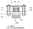
図1は、本発明の実施の形態1に係わる電子部品の実装構造体の断面模式図である。
図1に示すように、本実施の形態の電子部品の実装構造体100は、配線基板30と、配線基板30の回路パターンに実装された電子部品10と、電子部品10の両端に設けられた電極20と、電子部品10の回路パターン側の反対側の面に配設された伝熱材40と、伝熱材40の電子部品10との接触面(電子部品接触面と記す)の反対側の面(覆体接触面と記す)に配設された覆体50と、覆体50と配線基板30との間に設けられたスペーサ75と、覆体50をスペーサ75を介して配線基板30に固定する固定機構である、ボルト70とナット71とを備えており、覆体50が回路パターン面と平行に配線基板30に固定されている。
Embodiment 1 FIG.
FIG. 1 is a schematic cross-sectional view of a mounting structure for an electronic component according to Embodiment 1 of the present invention.
As shown in FIG. 1, the electronic
本実施の形態では、配線基板30は、表面に絶縁層を介して銅箔の回路パターンが形成されているアルミ基板である。
電子部品10は、抵抗やコンデンサの表面実装用チップ部品であり、その両端には、電極20が接続されており、電極20の一端は内側に折り曲げられており、折曲げられた部分が、配線基板30の回路パターンに半田で接合される回路接合部24aとなっている。
In the present embodiment, the
The
また、電極20には立脚部24bが設けられており、回路接合部24aと電子部品10の回路パターン側の面との間に空隙が形成されている。すなわち、電子部品10は、配線基板30から浮いた状態で実装されている。
また、電極20には、例えば、42アロイが用いられ、その幅は電子部品10の幅と同じとし、厚みはバネ性をもたせるため0.1〜0.2mmと薄くし、電子部品10を配線基板30から浮かせる立脚部24bの高さは、0.3mm〜1mm程度である。
Further, the
Further, for example, a 42 alloy is used for the
本実施の形態の電子部品の実装構造体100では、電子部品10が、立脚部24bが設けられた電極20を介して配線基板の回路パターンに接合されているので、電子部品10に、パッケージサイズの略称が3216、4532、5750のような大きいチップ部品を用いても、チップ部品に生じる熱応力を低減することができる。
また、電子部品10が、セラミックが主たる構成材料のコンデンサである場合、電極20を形成する材料に、5ppm/℃程度の低線膨張係数の42アロイを用いると、熱応力の低減に、特に有効である。また、電極20を形成する材料には、42アロイ以外に、いわゆるインバー合金が用いられ、同様に熱応力を低減することができる。
In the electronic
Further, when the
本実施の形態の電子部品の実装構造体100では、電子部品10の熱は、電極20を介して配線基板30に伝導し、配線基板30から放熱される以外に、電子部品10の伝熱材40との接触面(伝熱材接触面と記す)が伝熱材40を介して覆体50の内表面と接しているので、覆体50にも伝導し、覆体50の外表面から放熱される。放熱性の面から覆体50は金属であることが好ましい。
それと、覆体50に伝導した熱は、ボルト70を金属で形成することにより、配線基板30へ効率良く伝導でき、配線基板30から放熱される。
In the electronic
In addition, the heat conducted to the
本実施の形態では、電極20が薄板で形成されており、電極20の伝熱面積が小さいので、電極20を介して配線基板30に伝導する熱量は小さい。特に電極20に42アロイを用いた場合は、42アロイの熱伝導率が小さいので、配線基板30に伝導する熱量がさらに小さくなる。
しかし、本実施の形態の電子部品の実装構造体100は、電極以外にも電子部品の熱を伝導し外部に放熱する経路を有しており、放熱性が優れている。
In the present embodiment, since the
However, the electronic
本実施の形態の電子部品の実装構造体100では、配線基板30の回路パターン面と覆体50の内表面との間隔をスペーサ75で調整することにより、電子部品10と覆体50との間に設置された伝熱材40に加わる圧力を調整して、伝熱材40の電子部品接触面と電子部品10の伝熱材接触面との確実な接触、および、伝熱材40の覆体接触面と覆体50の内表面との確実な接触を実現し、電子部品10から覆体50への熱伝導における熱抵抗を低くすることにより、放熱性を向上させている。
In the electronic
また、覆体50から伝熱材40を介して電子部品10に加わる押圧力も調整できるので、この押圧力による電子部品の破壊も防止できる。
それと、電極20に立脚部24bが設けられており、立脚部24bはバネ性を有しているので、例え、覆体50から電子部品10への押圧力が過剰になっても、立脚部24bが押圧力を緩和するので、電子部品10の破壊を防止できる。
Moreover, since the pressing force applied to the
In addition, the
また、電子部品10は、伝熱材40を介して覆体50から押圧力が加えられ、伝熱材40を介してではあるが、覆体50で固定されているので、振動が加わっても、電子部品10が大きく振動するのが防止でき、耐振性が優れている。それと、スペーサ75を調整することにより、確実に押圧力を加えることができ、伝熱材40が、ずれたり外れたりすることも防止できる。
In addition, the
伝熱材40の厚みは、熱抵抗を下げるので、できるだけ薄い方が好ましい。
そこで、本実施の形態の電子部品の実装構造体では、配線基板30の回路パターン面から電子部品10の伝熱材接触面までの高さ(電子部品の設置高さと記す)と伝熱材40の厚みとの合計が、覆体50を配線基板30へ固定する前より、固定後の方が薄くなるように、スペーサ75の高さが調整されている。
すなわち、配線基板30の回路パターン形成面から配線基板30に固定した覆体50の伝熱材接触面である内表面までの間隔が、電子部品10の設置高さより大きく、覆体50を固定する前の電子部品10の設置高さと伝熱材40の厚みとの合計より小さくなるように、スペーサ75の高さが設定されている。
The thickness of the
Therefore, in the electronic component mounting structure according to the present embodiment, the height from the circuit pattern surface of the
That is, the distance from the circuit pattern forming surface of the
このような構造になっているので、覆体50を固定すると、覆体50が伝熱材40を電子部品10に押し付けるように圧力がかかり、伝熱材40がグリースや接着剤のように流動性のある材質の場合は、伝熱材40を排斥し、シートの場合は、伝熱材40を圧延して薄くして、伝熱材40の低熱抵抗化が図れる。併せて、電子部品10と伝熱材40との間、および伝熱材40と覆体50との間の、接触熱抵抗も低減でき、さらに放熱性を高めることができる。
付け加えて、個々の電子部品の実装のばらつきにより生じる高さの差も吸収でき、全ての接触箇所で放熱性を改善できる。
Since it has such a structure, when the
In addition, height differences caused by variations in mounting of individual electronic components can be absorbed, and heat dissipation can be improved at all contact points.
そして、伝熱材40に、可撓性のある材料を用い、そのバネ定数をバネ性のある電極20のバネ定数よりも小さく設定しておくと、伝熱材40の厚みを押圧力により薄くすることが容易に達成できる。
そのような、伝熱材40の材料としては、例えばシリコーンシートなどが挙げられ、熱伝導率6W/mK程度のものが好ましい。
If a flexible material is used for the
Examples of such a material for the
また、伝熱材40のバネ定数を電極20のものより小さくすると、例えば、伝熱材シートの厚みばらつきや実装後の電子部品の設置高さ変動を吸収するように、伝熱材40の厚みを大きくした場合でも、伝熱材40が大きく変形し、電極20の変形量が増大するのを抑え、電極20が破損するのを防止できる。
また、電子部品10が傾いて実装された場合に、覆体50を電子部品10に直接押し当てる構成の場合では、覆体50が電子部品10に片当たりするが、本実施の形態のように、伝熱材40を介在させることで片当たりが発生せず、片当たりによる応力の増大を防止し、電子部品10の破損を防ぐことができる。
Further, when the spring constant of the
In the case where the
図2は、本発明の実施の形態1に係わる電子部品の実装構造体において配線基板に放熱体を設けた状態を示す断面模式図である。
図2に示す、本実施の形態の電子部品の実装構造体100において、配線基板30の電子部品実装面の反対側の面にヒートシンク等の放熱体90を設けた電子部品の実装構造体100aは、配線基板30側の熱抵抗を小さくし、放熱性を高めることができる。
配線基板30と放熱体90の間には伝熱材を設けることが好ましく、また、ねじ止め等で配線基板30と放熱体90とを機械的に接続することにより、耐振性を向上することができる。
FIG. 2 is a schematic cross-sectional view showing a state in which a radiator is provided on the wiring board in the electronic component mounting structure according to Embodiment 1 of the present invention.
In the electronic
It is preferable to provide a heat transfer material between the
本実施の形態の電子部品の実装構造体100と100aとは、電子部品の設置高さと伝熱材40の厚みとの合計が、覆体50を配線基板30へ固定する前より、固定後の方が薄くなるように設定されており、常時、押圧力が電子部品および伝熱材にかけられた状態となり、振動が加わっても振動エネルギが減衰し、不必要な共振により電子部品の振幅が増大するのを防止できる。
また、伝熱材40が電子部品10と覆体50との間に介在するので、覆体50が電子部品10に片当たりして擦れるなどの不具合が防止できる。
In the electronic
In addition, since the
本実施の形態では、配線基板30と覆体50との固定は、ねじ止めとしたが、スペーサを設けておけば、覆体50を配線基板30に対して圧力をかけることができる固定法で良く、圧入やパッチン止め、板バネによる固定が挙げられ、押え機構を設けても良い。
また、配線基板30の覆体50への固定が、ねじ止めの場合、ねじ70の締め付けトルクで伝熱材40の厚み管理ができるなら、スペーサ75を省略しても良い。
In this embodiment, the
In addition, when fixing the
図3は、参考の形態に係わる電子部品の実装構造体の断面模式図である。
図3に示すように、電子部品の実装構造体200は、配線基板30と、配線基板30の回路パターンに実装された、第1の電子部品10aと第2の電子部品11と第3の電子部品12と、第1の電子部品10aの両端に設けられた電極20aと、各電子部品が搭載された配線基板30を固定した筐体本体60と、筐体本体60の蓋となる覆体50aと、覆体50aと第1の電子部品10aとの間に配設された伝熱材40とを備えている。
すなわち、電子部品を実装した配線基板30は、筐体本体60と覆体50aとで形成される筐体に収納されている。
FIG. 3 is a schematic cross-sectional view of an electronic component mounting structure according to a reference embodiment.
As shown in FIG. 3, the electronic
That is, the
筐体本体60は、配線基板30を搭載した部分(基板搭載部と記す)60bと基板搭載部60bの周囲に設けられた壁である周壁部60aとを備えており、覆体50aが、周壁部60aの上面に接するとともに、配線基板30の回路パターンに対して平行に、配置されている。
伝熱材40は、覆体50aの内表面と第1の電子部品10aの伝熱材接触面との間に、これらの面と接して配設されている。
The housing
The
図3において、配線基板30は、表面に絶縁層を介して銅箔で回路パターンが形成されているアルミ基板である。
筐体本体60は、フィン61が設けられており、電子部品が搭載された配線基板30からの熱を放熱する放熱体でもあり、金属で形成されるのが好ましい。
覆体50aも、放熱性の面から金属であることが好ましい。
伝熱材40は、実施の形態1のものと同様である。
In FIG. 3, a
The
The
The
第2の電子部品11は、半導体素子をパッケージングした部品であり、半田接合面全体に電極を形成しており、耐熱応力性が高い。
第3の電子部品12は、パッケージサイズの略称が1005、1608、2012のような、小さいチップ部品であり、耐熱応力性が高く、チップ部品本体の側面から裏面および表面にかけて設けられた電極21を配線基板30に半田付けしても問題なく使用できる。
第1の電子部品10aは、実施の形態1における電子部品10と同様の、パッケージサイズの略称が3216、4532、5750等である、大きいな抵抗やコンデンサ等のチップ部品である。
第1の電子部品10aの電極20aの構造も、実施の形態1における電子部品10の電極20の構造と同様である。
The second
The third
The first
The structure of the
図3において、配線基板30は筐体本体60に、ねじ73等により機械的に固定されているが、配線基板30と筐体本体60との接触熱抵抗を小さくするため、配線基板30と筐体本体60との間に伝熱材を設けて固定しても良い。
また、覆体50aは、筐体本体60の周壁部60aの上面に、ねじ72等の固定機構により機械的に固定されており、蓋である覆体50aとケース本体である筐体本体60とで、ケースを形成している。
また、覆体50aは、配線基板30の回路パターン形成面と平行になっているので、筐体本体60の周壁部60aにより、覆体50aの内表面と配線基板30の回路パターン形成面との間隔が規定されている。
In FIG. 3, the
The
Further, since the
そして、図3に示された電子部品の実装構造体200でも、第1の電子部品10aの設置高さと伝熱材40の厚みとの合計が、覆体50aを周壁部60aへ固定する前より、固定後の方が薄くなるように、周壁部60aの高さが調整されている。
すなわち、配線基板30の回路パターン形成面から周壁部60aに固定された覆体50aの伝熱材接触面である内表面までの間隔(配線基板から覆体までの間隔と記す)が、第1の電子部品10aの設置高さより大きく、覆体50aを固定する前の第1の電子部品10aの設置高さと伝熱材40の厚みとの合計より小さくなるように、周壁部60aの高さが設定されている。
図3においても、伝熱材40には、流動性のあるグリースや接着剤、あるいは、押圧されて薄くなるシートが用いられる。
Also in the electronic
That is, the distance from the circuit pattern forming surface of the
Also in FIG. 3, the
サイズが大きく発熱量が大きいチップ部品である第1の電子部品10aは、その電極構造が実施の形態1における電子部品10の電極構造と同様であり、部品にかかる熱応力を低減できるようになっている。
そのため、第1の電子部品10aから配線基板まで、すなわち、第1の電子部品10aから放熱体である筐体本体60までの熱抵抗が大きく、この熱伝導経路による放熱は不十分である。
The first
Therefore, the thermal resistance from the first
しかし、図3に示された電子部品の実装構造体200では、配線基板30から覆体50aまでの間隔が、上記のようになっているので、第1の電子部品10aからの熱は、伝熱材40を介して覆体50aまで伝導され、覆体50aの外表面から放熱することができる。それと、覆体50aに伝導した熱は、筐体本体60へも伝導され、筐体本体60からも放熱される。
However, in the electronic
また、配線基板30から覆体50aまでの間隔が、上記のようになっているので、第1の電子部品10aは、伝熱材40を介して覆体50aから押圧力が加えられ、伝熱材40を介してではあるが、覆体50aで固定されており、耐振性が優れている。それと、周壁部60aの高さを調整することにより、確実に押圧力を加えることができ、伝熱材40がずれたり外れたりすることも防止できる。
また、第1の電子部品10aの電極構造が実施の形態1の電子部品10の電極構造と同様であるので、第1の電子部品10aに覆体50aから加わる押圧力を、バネ性がある立脚部で緩和でき、第1の電子部品10aの破壊を防止できる。
また、覆体50aが第1の電子部品10aに片当たりするのも防止できる。
In addition, since the distance from the
Further, since the electrode structure of the first
Further, it is possible to prevent the
図3においては、配線基板30に、放熱性が高いのでアルミ基板を用いているが、樹脂を用いたプリント基板やセラミック基板でも良い。
プリント基板の場合、筐体本体60からの放熱性を高めるために、発熱部品直下にスルーホールや銅柱などを設けて熱抵抗を下げるのが好ましい。しかし、配線基板30の裏面に電極があり、この電極と筐体本体60との電位が異なる場合は、配線基板30と筐体本体60との間に絶縁層を設ける。
In FIG. 3, an aluminum substrate is used for the
In the case of a printed circuit board, in order to improve the heat dissipation from the
また、樹脂を用いたプリント基板や、低熱伝導率のセラミック材で形成されたセラミック基板の場合は、第1の電子部品10aから、放熱体でもある筐体本体60までの熱抵抗が、さらに増大するので、第1の電子部品の熱を覆体50aから放熱する本構成が特に有効となる。
図3では、配線基板30に電子部品を搭載しているが、筐体本体60の表面に絶縁層を介して銅箔による回路パターンを形成し、この回路パターンに電子部品を搭載しても良い。この場合は、特に、第2の電子部品11や第3の電子部品12の放熱性が向上する。
Further, in the case of a printed circuit board using a resin or a ceramic substrate formed of a ceramic material with low thermal conductivity, the thermal resistance from the first
In FIG. 3, electronic components are mounted on the
図3では、第1の電子部品10aに伝熱材が設けられているが、第2の電子部品11や第3の電子部品12に伝熱材を設けて、これらの電子部品の熱を覆体に伝導し、覆体から放熱しても良い。
図3では、配線基板30の筐体本体60への固定、および、覆体50aの筐体本体60への固定は、ねじ止めとしたが、配線基板30を筐体本体60に圧力をかける固定法、および、覆体50aを筐体本体60に対して圧力をかける固定法を用いることができ、このような固定法として、圧入やパッチン止め、板バネによる固定が挙げられ、押え機構を設けても良い。
In FIG. 3, the first
In FIG. 3, the
図4は、参考の形態に係わる電子部品の実装構造体の断面模式図である。
図4に示すように、電子部品の実装構造体300は、覆体に、伝熱材40との接触部の反対側である外表面にフィン51が設けられた覆体50bを用いた以外、図3に示された電子部品の実装構造体と同様であり、図3に示された電子部品の実装構造体と同様な効果を有する。
また、覆体の伝熱材40との接触部の反対側にフィン51が設けられているので、放熱性が向上している。
それと、フィン51が覆体の補強にもなるので、覆体の厚みを薄くすることができる。
FIG. 4 is a schematic cross-sectional view of an electronic component mounting structure according to a reference embodiment .
As shown in FIG. 4, the electronic
Moreover, since the
And since the
フィン51は、伝熱材を介して覆体にねじ止めなどで機械的に接続しても良いが、覆体とフィンを一体に成型することが、効率的であり、且つ熱抵抗を下げるので好ましい。
図4では、フィン51が、覆体の発熱する電子部品の周辺のみに設けられているが、覆体全域の外表面に設けても良い。
覆体の伝熱材との接触部の反対側にフィンを設けることは、実施の形態1の電子部品の実装構造体にも適用でき、同様な効果を有する。
The
In FIG. 4, the
Providing the fin on the opposite side of the contact portion of the cover with the heat transfer material can also be applied to the electronic component mounting structure of Embodiment 1 and has the same effect.
図5は、参考の形態に係わる電子部品の実装構造体の断面模式図である。
図5に示すように、電子部品の実装構造体400は、覆体に、内表面における第1の電子部品10aが投影される部分に、第1の突出部53が設けられた覆体50cが用いられ、配線基板30の回路パターン形成面から周壁部60aに固定された覆体50cの伝熱材接触面である第1の突出部53の表面までの間隔が、第1の電子部品10aの設置高さより大きく、覆体50cを固定する前の第1の電子部品10aの設置高さと伝熱材40の厚みとの合計より小さくなるように、周壁部60aの高さが設定されている以外、図3に示された電子部品の実装構造体と同様であり、図3に示された電子部品の実装構造体と同様な効果を有する。
FIG. 5 is a schematic cross-sectional view of an electronic component mounting structure according to a reference embodiment.
As shown in FIG. 5, the electronic
電子部品の実装構造体400は、覆体50cが、内表面の第1の電子部品10aの投影部に第1の突出部53が設けられているので、図5に示すように配線基板30に、第1の電子部品10aの設置高さより、かなり高い電子部品13が搭載されていても、第1の電子部品10aと覆体50cとの間に配設される伝熱材40の厚みを薄くでき、第1の電子部品10aの熱を覆体へ伝導する伝導路の熱抵抗が増大するのが防止できる。
In the electronic
図5において、第1の突出部53の伝熱材40との接触面のサイズは、第1の電子部品10aの伝熱材接触面のサイズより大きめになっており、覆体50cにおける第1の突出部53の周囲に向かって熱を広げることができ、放熱性を高めることができる。
図示しないが、図4に示すように、覆体における、伝熱材との接触部の反対側の外表面にフィンを設けても良い。
In FIG. 5, the size of the contact surface of the first projecting
Although not shown, as shown in FIG. 4 , fins may be provided on the outer surface of the cover opposite to the contact portion with the heat transfer material.
図6は、別の参考の形態に係わる電子部品の実装構造体における、別の形状の第1の突出部が設けられた覆体を説明する図である。
図6に示すように、別の形状の第1の突出部が設けられた覆体50dは、肉厚を大きく変化させずに覆体を塑性変形させて形成した第1の突出部54を備えたものである。この第1の突出部54はプレス加工により形成でき、覆体の製造が容易である。
FIG. 6 is a diagram for explaining a cover provided with a first protrusion having a different shape in an electronic component mounting structure according to another reference embodiment.
As shown in FIG. 6, the
図示しないが、第1の突出部は、覆体における、第1の電子部品が投影される部分に加え、他の電子部品が投影される部分にも設けても良く、この場合、この突出部と他の電子部品との間に伝熱材を配設して、他の電子部品の熱を覆体から放熱することもできる。 Although not shown, the first protrusion may be provided on a portion of the cover where the first electronic component is projected, as well as on a portion where another electronic component is projected. It is also possible to dissipate heat from the cover by disposing a heat transfer material between the cover and the other electronic component.
図7は、別の参考の形態に係わる電子部品の実装構造体における覆体を説明する、上面模式図(a)と側面模式図(b)とである。
図7に示す電子部品の実装構造体は、覆体に、覆体50cの第1の突出部53の三方の周囲に、第1の突出部53を囲んで、貫通孔80が設けられた覆体50eを用いた以外、図5に示す電子部品の実装構造体と同様である。
FIG. 7 is a schematic top view (a) and a schematic side view (b) for explaining a cover in a mounting structure for an electronic component according to another reference embodiment.
The electronic component mounting structure shown in FIG. 7 is a cover in which a through
図8は、別の参考の形態に係わる電子部品の実装構造体における、別例の覆体を説明する側面模式図である。
図8に示す電子部品の実装構造体は、覆体に、覆体50dの第1の突出部54の三方の周囲に、第1の突出部54を囲んで、貫通孔80が設けられた覆体50fを用いた以外、図5に示す電子部品の実装構造体400と同様である。
FIG. 8 is a schematic side view illustrating another example of the cover in the electronic component mounting structure according to another reference embodiment.
The electronic component mounting structure shown in FIG. 8 has a cover in which a through-
図8に示す形態では、覆体の第1の突出部の三方の周囲に、第1の突出部を囲んで貫通孔が設けられているので、覆体の伝熱材を介して第1の電子部品に押圧力を加える部分がバネ性を有することとなり、第1の電子部品に加わる応力を緩和できる。
また、第1の電子部品の周囲の対流を促進して放熱性を向上することもできる。
In the form shown in FIG. 8, since the through-hole is provided around the first protrusion of the cover so as to surround the first protrusion, the first protrusion is interposed via the heat transfer material of the cover. The portion to which the pressing force is applied to the electronic component has a spring property, and the stress applied to the first electronic component can be relaxed.
In addition, heat dissipation can be improved by promoting convection around the first electronic component.
実施の形態2.
図9は、本発明の実施の形態2に係わる電子部品の実装構造体における覆体を説明する、内表面模式図(a)と側面模式図(b)とである。
図9に示す本実施の形態の電子部品の実装構造体は、覆体に、覆体50aの内表面に第1の電子部品10aの外周を囲むように形成された第2の突出部55が設けられた覆体50gを用いた以外、図3に示された電子部品の実装構造体と同様である。
Embodiment 2. FIG.
FIGS. 9A and 9B are an inner surface schematic diagram (a) and a side surface schematic diagram (b) for explaining a cover in the electronic component mounting structure according to the second embodiment of the present invention .
The electronic component mounting structure according to the present embodiment shown in FIG. 9 has a
この覆体50gを用いた電子部品の実装構造体では、伝熱材40の位置決めが容易になり生産性が向上するとともに、伝熱材40のずれが防止でき長期信頼性が向上する。
図9(b)に示すように、第2の突出部55をフィン構造にすると放熱性も向上する。
この覆体の構造は、実施の形態1や図4に示された電子部品の実装構造体にも適用できる。
In the electronic component mounting structure using the
As shown in FIG. 9B, when the
This cover structure can also be applied to the electronic component mounting structure shown in the first embodiment or FIG .
図10は、本発明の実施の形態2に係わる電子部品の実装構造体における、別例の覆体を説明する側面模式図である。
図10に示す本実施の形態の電子部品の実装構造体は、覆体に、覆体50aの外表面に厚み方向の溝56を形成し、覆体50aの内表面側に突部を、第1の電子部品10aの外周を囲むように設けた覆体50hを用いた以外、図3に示された電子部品の実装構造体と同様である。
FIG. 10 is a schematic side view illustrating another example of the cover in the electronic component mounting structure according to Embodiment 2 of the present invention .
In the electronic component mounting structure according to the present embodiment shown in FIG. 10, a
この覆体50hを用いた電子部品の実装構造体では、伝熱材40の位置決めが容易になり生産性が向上するとともに、覆体における、伝熱材を介して第1の電子部品に押圧力を加える部分がバネ性を有することとなり、第1の電子部品に加わる応力を緩和できる。
この覆体の構造は、実施の形態1の電子部品の実装構造体にも適用できる。
In the electronic component mounting structure using the
This cover structure can also be applied to the electronic component mounting structure of the first embodiment.
実施の形態3.
図11は、本発明の実施の形態3に係わる電子部品の実装構造体で用いられる覆体の伝熱材接触面の状態を示す断面模式図である。
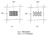
図12は、本発明の実施の形態3における覆体の伝熱材接触面に形成された、第1の形状の突起部(a)と第2の形状の突起部(b)とを示す平面模式図である。
Embodiment 3 FIG.
FIG. 11: is a cross-sectional schematic diagram which shows the state of the heat-transfer material contact surface of the cover used with the mounting structure of the electronic component concerning Embodiment 3 of this invention.
FIG. 12 is a plan view showing a first shape protrusion (a) and a second shape protrusion (b) formed on the heat transfer material contact surface of the cover according to Embodiment 3 of the present invention. It is a schematic diagram.
図11に示すように、本実施の形態の電子部品の実装構造体は、覆体が、伝熱材接触面に複数の細かい突起部52が設けられた覆体50iである以外、実施の形態1の電子部品の実装構造体と同様である。
そして、伝熱材接触面の突起部52の形状は、例えば、図12(a)に示す溝状突起部521や図12(b)に示すバンプ状突起部522が挙げられる。
As shown in FIG. 11, the electronic component mounting structure according to the present embodiment is the same as the embodiment except that the cover is a
And as for the shape of the
本実施の形態のような、伝熱材接触面に突起部52が形成された覆体50iでは、覆体50iで伝熱材40を押圧した時、伝熱材がグリースや接着剤等の流動性のものの場合、伝熱材の排斥効果が高まるとともに、伝熱材の領域に熱伝導性が高い覆体が混在する状態となり、熱抵抗を低減することがで、放熱性を高めることができる。
また、伝熱材がシートの場合、伝熱材を薄く延ばすことに加え、やはり伝熱材の領域に熱伝導性が高い覆体が混在する状態となり、熱抵抗を低減することができ、放熱性を高めることができる。
In the
In addition, when the heat transfer material is a sheet, in addition to extending the heat transfer material thinly, the heat transfer material region also contains a cover with high thermal conductivity, which can reduce the thermal resistance and release heat. Can increase the sex.
覆体50iの突起部52は、先端が平坦でも良いが、図11に示すように、先端を細くした方が、効果が大であり好ましい。
また、突起部52が溝状突起部521である場合、溝の方向は電子部品10の短手方向が好ましい。
そして、突起部52は、覆体50iの製造時に同時に形成することができる。
本実施の形態の複数の細かい突起部が設けられた覆体は、実施の形態2の覆体として適用でき、同様な効果を有する。
The
When the
And the
The cover provided with a plurality of fine protrusions of the present embodiment can be applied as the cover of the second embodiment and has the same effect.
実施の形態4.
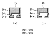
図13は、本発明の実施の形態4に係わる電子部品の実装構造体における電子部品の、第1の形状の電極(a)と第2の形状の電極(b)とを示す正面模式図である。
図13に示すように、本実施の形態の電子部品の実装構造体は、電子部品10の電極における立脚部が屈曲している以外、実施の形態1の電子部品の実装構造体と同様である。
Embodiment 4 FIG.
FIG. 13: is a front schematic diagram which shows the electrode (a) of a 1st shape, and the electrode (b) of a 2nd shape of the electronic component in the mounting structure of the electronic component concerning Embodiment 4 of this invention. is there.
As shown in FIG. 13, the electronic component mounting structure according to the present embodiment is the same as the electronic component mounting structure according to the first embodiment, except that standing legs of the electrodes of the
すなわち、本実施の形態における、第1の形状の電極は、図13(a)に示すように、立脚部24bが一定の角度で内側に屈曲した電極20bであり、第2の形状の電極は、図13(b)に示すように、立脚部24bがくの字状に内側に屈曲した電極20cである。
That is, in the present embodiment, as shown in FIG. 13A, the first shape electrode is an
本実施の形態の電子部品の実装構造体は、実施の形態1の電子部品の実装構造体と同様な効果を有するとともに、電子部品の電極が上記のような形状であるので、立脚部24bのバネ性が高く、押圧力を緩和する能力が大きく、電子部品10の破壊を防止する効果が大きい。
本実施の形態の電子部品の電極は、実施の形態2及び実施の形態3の、電子部品あるいは第1の電子部品の電極にも適用でき、同様な効果を有する。
The electronic component mounting structure according to the present embodiment has the same effects as the electronic component mounting structure according to the first embodiment, and the electrodes of the electronic component have the above-described shape. The spring property is high, the ability to relieve the pressing force is large, and the effect of preventing the
The electrode of the electronic component of the present embodiment can be applied to the electrode of the electronic component or the first electronic component of the second and third embodiments, and has the same effect.
実施の形態5.
図14は、本発明の実施の形態5に係わる電子部品の実装構造体における電子部品の、第1の形状の電極(a)と第2の形状の電極(b)とを示す側面模式図である。
本実施の形態の電子部品の実装構造体は、電子部品10の各端部に接合された電極に、第1の形状の電極として図14(a)に示した、長手方向で分割されている電極20d、あるいは、第2の形状の電極として図14(b)に示した、回路接合部と電子部品との接合部とが、長手方向で分割されている電極20eを用いた以外、実施の形態1の電子部品の実装構造体と同様である。
Embodiment 5 FIG.
FIG. 14 is a schematic side view showing the first shape electrode (a) and the second shape electrode (b) of the electronic component in the electronic component mounting structure according to Embodiment 5 of the present invention. is there.
The electronic component mounting structure according to the present embodiment is divided in the longitudinal direction as shown in FIG. 14A as an electrode having a first shape on the electrodes joined to the respective end portions of the
本実施の形態の電子部品の実装構造体は、実施の形態1の電子部品の実装構造体と同様な効果を有するとともに、電子部品10が、図14(a)あるいは図14(b)にあるように、少なくとも電極の電子部品との接合部と回路接合部とが、電極の長手方向で分割されており、電極の配線基板30に半田接合する面積が広くなり熱応力が増大する場合でも、熱応力を緩和することができる。
本実施の形態では、電極全体あるいは局部の分割は2分割であるが、加工が可能であれば、これに限定されない。
本実施の形態の電子部品の電極は、実施の形態2〜実施の形態4の、電子部品あるいは第1の電子部品の電極として適用でき、同様な効果を有する。
The electronic component mounting structure of the present embodiment has the same effect as the electronic component mounting structure of the first embodiment, and the
In the present embodiment, the whole electrode or the local division is divided into two, but it is not limited to this as long as processing is possible.
The electrode of the electronic component of the present embodiment can be applied as the electrode of the electronic component or the first electronic component of Embodiments 2 to 4 , and has the same effect.
本発明に係わる電子部品の実装構造体は、配線基板に搭載されたチップ部品に加わる熱応力を低減するとともに、このチップ部品からの熱を効率よく放熱するものであり、高温環境で使用される機器に用いられる。 The electronic component mounting structure according to the present invention reduces thermal stress applied to the chip component mounted on the wiring board and efficiently radiates heat from the chip component, and is used in a high temperature environment. Used for equipment.
10 電子部品、10a 第1の電子部品、11 第2の電子部品、
12 第3の電子部品、13 電子部品、
20,20a,20b,20c,20d,20e,21 電極、
24a 回路接合部、24b 立脚部、30 配線基板、40 伝熱材、
50,50a,50b,50c,50d,50e,50f,50g 覆体、
50h,50i 覆体、51 フィン、52 突起部、521 溝状突起部、
522 バンプ状突起部、53,54 第1の突出部、55 第2の突出部、56 溝、60 筐体本体、60a 周壁部、60b 基板搭載部、61 フィン、70 ボルト、71 ナット、72,73 ねじ、75 スペーサ、80 貫通孔、90 放熱体、
100,100a,200,300,400 電子部品の実装構造体。
10 electronic component, 10a first electronic component, 11 second electronic component,
12 Third electronic component, 13 Electronic component,
20, 20a, 20b, 20c, 20d, 20e, 21 electrodes,
24a circuit junction part, 24b stand part, 30 wiring board, 40 heat transfer material,
50, 50a, 50b, 50c, 50d, 50e, 50f, 50g
50h, 50i Cover, 51 fin, 52 projection, 521 groove projection,
522 Bump-like protrusion, 53, 54 First protrusion, 55 Second protrusion, 56 groove, 60 Housing body, 60a Perimeter wall, 60b Substrate mounting part, 61 Fin, 70 Bolt, 71 Nut, 72, 73 screws, 75 spacers, 80 through holes, 90 heat sinks,
100, 100a, 200, 300, 400 Electronic component mounting structure.
Claims (9)
上記電子部品がチップ部品であり、上記電極が、上記回路パターンと接合する回路接合部と、上記電子部品を上記回路パターンから浮かすとともにバネ性がある立脚部とを有しており、上記回路パターン面から上記電子部品の伝熱材側の面までの高さである電子部品の設置高さと上記伝熱材の厚みとの合計が、上記覆体を固定する前より、固定後の方が薄くなっており、上記伝熱材のばね定数が上記電極のばね定数よりも小さくなっており、
上記覆体が、スペーサを介して上記配線基板に、金属のボルトとナットとで固定されており、上記配線基板の回路パターン形成面から上記覆体の内表面までの間隔が、上記電子部品の設置高さより大きく、上記覆体を固定する前の上記電子部品の設置高さと上記伝熱材の厚みとの合計より小さくなるように、上記スペーサの高さを設定した電子部品の実装構造体。 A wiring board; an electronic component mounted on the circuit pattern of the wiring board; electrodes provided on both ends of the electronic component; and heat transfer disposed on a surface of the electronic component opposite to the circuit pattern side. A mounting structure for an electronic component comprising: a cover that is in contact with a surface of the heat transfer material opposite to the contact surface with the electronic component and is fixed in parallel to the circuit pattern. And
The electronic component is a chip component, and the electrode has a circuit joint portion that joins the circuit pattern, and a standing leg portion that floats the electronic component from the circuit pattern and has a spring property. The total height of the electronic component, which is the height from the surface to the heat transfer material side surface of the electronic component, and the thickness of the heat transfer material is thinner after fixing than before fixing the cover. The spring constant of the heat transfer material is smaller than the spring constant of the electrode,
The cover is fixed to the wiring board via a spacer with metal bolts and nuts, and the distance from the circuit pattern forming surface of the wiring board to the inner surface of the cover is such that the electronic component An electronic component mounting structure in which a height of the spacer is set to be smaller than a total of an installation height of the electronic component before fixing the cover and a thickness of the heat transfer material.
Priority Applications (1)
| Application Number | Priority Date | Filing Date | Title |
|---|---|---|---|
| JP2011096111A JP5936313B2 (en) | 2011-04-22 | 2011-04-22 | Electronic component mounting structure |
Applications Claiming Priority (1)
| Application Number | Priority Date | Filing Date | Title |
|---|---|---|---|
| JP2011096111A JP5936313B2 (en) | 2011-04-22 | 2011-04-22 | Electronic component mounting structure |
Publications (3)
| Publication Number | Publication Date |
|---|---|
| JP2012227472A JP2012227472A (en) | 2012-11-15 |
| JP2012227472A5 JP2012227472A5 (en) | 2013-11-28 |
| JP5936313B2 true JP5936313B2 (en) | 2016-06-22 |
Family
ID=47277278
Family Applications (1)
| Application Number | Title | Priority Date | Filing Date |
|---|---|---|---|
| JP2011096111A Active JP5936313B2 (en) | 2011-04-22 | 2011-04-22 | Electronic component mounting structure |
Country Status (1)
| Country | Link |
|---|---|
| JP (1) | JP5936313B2 (en) |
Cited By (1)
| Publication number | Priority date | Publication date | Assignee | Title |
|---|---|---|---|---|
| CN110678032A (en) * | 2019-11-01 | 2020-01-10 | 珠海格力电器股份有限公司 | Electrical apparatus box and air conditioner |
Families Citing this family (13)
| Publication number | Priority date | Publication date | Assignee | Title |
|---|---|---|---|---|
| JP5949681B2 (en) * | 2013-06-25 | 2016-07-13 | 株式会社豊田自動織機 | Electric compressor |
| JP6453195B2 (en) * | 2015-09-29 | 2019-01-16 | 日立オートモティブシステムズ株式会社 | In-vehicle control device |
| JP6672724B2 (en) * | 2015-11-10 | 2020-03-25 | Tdk株式会社 | Power supply |
| JP6402942B2 (en) | 2015-12-11 | 2018-10-10 | 株式会社オートネットワーク技術研究所 | Electrical junction box |
| WO2017098899A1 (en) * | 2015-12-11 | 2017-06-15 | 株式会社オートネットワーク技術研究所 | Electrical junction box |
| JP2018034587A (en) * | 2016-08-30 | 2018-03-08 | ダイキョーニシカワ株式会社 | Heat radiation structure of component to be connected |
| JP2018098927A (en) * | 2016-12-14 | 2018-06-21 | 株式会社オートネットワーク技術研究所 | Electric connection box |
| JP6958438B2 (en) | 2018-03-08 | 2021-11-02 | 株式会社デンソー | Heat dissipation device for electronic components |
| JP7124795B2 (en) * | 2019-06-27 | 2022-08-24 | 株式会社村田製作所 | Electronic component module, electronic component unit, and electronic component module manufacturing method |
| JP7452184B2 (en) | 2020-03-30 | 2024-03-19 | 富士電機株式会社 | power converter |
| JP7152465B2 (en) * | 2020-12-16 | 2022-10-12 | Necプラットフォームズ株式会社 | cooling structure and computer |
| KR20230026887A (en) * | 2021-08-18 | 2023-02-27 | 현대자동차주식회사 | Inverter apparatus for mobility |
| JP2024037427A (en) * | 2022-09-07 | 2024-03-19 | ヤマハ発動機株式会社 | electric vehicle |
Family Cites Families (14)
| Publication number | Priority date | Publication date | Assignee | Title |
|---|---|---|---|---|
| JPH0747902Y2 (en) * | 1989-03-30 | 1995-11-01 | ローム株式会社 | Mounting device for mounting chip type electronic components |
| JPH06104139A (en) * | 1992-09-21 | 1994-04-15 | Matsushita Electric Ind Co Ltd | Ceramic chip part |
| JPH1065385A (en) * | 1996-08-21 | 1998-03-06 | Mitsubishi Electric Corp | Substrate case structure |
| JPH1145821A (en) * | 1997-07-25 | 1999-02-16 | Tdk Corp | Composite laminated ceramic capacitor having metal terminals |
| JP3492504B2 (en) * | 1997-11-28 | 2004-02-03 | エヌイーシーコンピュータテクノ株式会社 | Heat dissipation device for electronic components |
| JP4023054B2 (en) * | 1999-12-07 | 2007-12-19 | 株式会社デンソー | Electronic circuit unit |
| JP4273673B2 (en) * | 2001-03-19 | 2009-06-03 | 株式会社デンソー | Heating element mounting structure |
| JP2004186294A (en) * | 2002-12-02 | 2004-07-02 | Denso Corp | Electronic apparatus |
| JP4860552B2 (en) * | 2007-06-08 | 2012-01-25 | 日本オプネクスト株式会社 | Semiconductor device |
| JP4796999B2 (en) * | 2007-07-17 | 2011-10-19 | 日立オートモティブシステムズ株式会社 | Electronic control unit |
| JP4400662B2 (en) * | 2007-09-12 | 2010-01-20 | 株式会社デンソー | Electronic circuit component mounting structure |
| JP2009176990A (en) * | 2008-01-25 | 2009-08-06 | Panasonic Corp | Electronic device unit |
| JP5045649B2 (en) * | 2008-11-17 | 2012-10-10 | 株式会社村田製作所 | Ceramic capacitor and electronic component including the same |
| JP5353251B2 (en) * | 2009-01-07 | 2013-11-27 | Tdk株式会社 | Multilayer capacitor and multilayer capacitor mounting structure |
-
2011
- 2011-04-22 JP JP2011096111A patent/JP5936313B2/en active Active
Cited By (1)
| Publication number | Priority date | Publication date | Assignee | Title |
|---|---|---|---|---|
| CN110678032A (en) * | 2019-11-01 | 2020-01-10 | 珠海格力电器股份有限公司 | Electrical apparatus box and air conditioner |
Also Published As
| Publication number | Publication date |
|---|---|
| JP2012227472A (en) | 2012-11-15 |
Similar Documents
| Publication | Publication Date | Title |
|---|---|---|
| JP5936313B2 (en) | Electronic component mounting structure | |
| US9271427B2 (en) | Flexible thermal transfer strips | |
| JP2009117612A (en) | Circuit module and method of manufacturing the same | |
| WO2007105580A1 (en) | Base for power module | |
| JP2014036033A (en) | Semiconductor device | |
| JP2002217343A (en) | Electronic device | |
| JP4402602B2 (en) | Capacitor cooling structure and power conversion device | |
| WO2009110045A1 (en) | Structure for attaching component having heating body mounted thereon | |
| TW200836044A (en) | Heat-dissipating module | |
| JP6048238B2 (en) | Electronic equipment | |
| JP5640616B2 (en) | Heat dissipation structure for electronic components | |
| WO2014140098A1 (en) | Heat spreader with flat pipe cooling element | |
| JP2005012127A (en) | Electronic control apparatus | |
| WO2012164756A1 (en) | Radiator structure | |
| JP4046623B2 (en) | Power semiconductor module and fixing method thereof | |
| JP2020061482A (en) | Heat dissipation structure | |
| JP2010021410A (en) | Thermo-module | |
| WO2021145096A1 (en) | Electronic device | |
| JP2008227043A (en) | Radiating substrate and power source unit using the same | |
| JP5669657B2 (en) | Semiconductor device | |
| WO2023112709A1 (en) | Mounting board, and electric apparatus equipped with mounting board | |
| CN213716878U (en) | Packaging structure | |
| JP6060053B2 (en) | Power semiconductor device | |
| WO2023090102A1 (en) | Mounting board and electrical equipment having mounting board installed thereon | |
| JP2004165251A (en) | Radiating device for electronic component |
Legal Events
| Date | Code | Title | Description |
|---|---|---|---|
| A521 | Request for written amendment filed |
Free format text: JAPANESE INTERMEDIATE CODE: A523 Effective date: 20131011 |
|
| A621 | Written request for application examination |
Free format text: JAPANESE INTERMEDIATE CODE: A621 Effective date: 20131011 |
|
| A977 | Report on retrieval |
Free format text: JAPANESE INTERMEDIATE CODE: A971007 Effective date: 20140519 |
|
| A131 | Notification of reasons for refusal |
Free format text: JAPANESE INTERMEDIATE CODE: A131 Effective date: 20140617 |
|
| A521 | Request for written amendment filed |
Free format text: JAPANESE INTERMEDIATE CODE: A523 Effective date: 20140731 |
|
| A02 | Decision of refusal |
Free format text: JAPANESE INTERMEDIATE CODE: A02 Effective date: 20150106 |
|
| A521 | Request for written amendment filed |
Free format text: JAPANESE INTERMEDIATE CODE: A523 Effective date: 20150227 |
|
| A911 | Transfer to examiner for re-examination before appeal (zenchi) |
Free format text: JAPANESE INTERMEDIATE CODE: A911 Effective date: 20150309 |
|
| A912 | Re-examination (zenchi) completed and case transferred to appeal board |
Free format text: JAPANESE INTERMEDIATE CODE: A912 Effective date: 20150417 |
|
| A521 | Request for written amendment filed |
Free format text: JAPANESE INTERMEDIATE CODE: A523 Effective date: 20151110 |
|
| A521 | Request for written amendment filed |
Free format text: JAPANESE INTERMEDIATE CODE: A523 Effective date: 20160202 |
|
| A521 | Request for written amendment filed |
Free format text: JAPANESE INTERMEDIATE CODE: A523 Effective date: 20160324 |
|
| A61 | First payment of annual fees (during grant procedure) |
Free format text: JAPANESE INTERMEDIATE CODE: A61 Effective date: 20160510 |
|
| R150 | Certificate of patent or registration of utility model |
Ref document number: 5936313 Country of ref document: JP Free format text: JAPANESE INTERMEDIATE CODE: R150 |
|
| R250 | Receipt of annual fees |
Free format text: JAPANESE INTERMEDIATE CODE: R250 |
|
| R250 | Receipt of annual fees |
Free format text: JAPANESE INTERMEDIATE CODE: R250 |
|
| R250 | Receipt of annual fees |
Free format text: JAPANESE INTERMEDIATE CODE: R250 |
|
| R250 | Receipt of annual fees |
Free format text: JAPANESE INTERMEDIATE CODE: R250 |
|
| R250 | Receipt of annual fees |
Free format text: JAPANESE INTERMEDIATE CODE: R250 |