JP5898955B2 - プロセスキットリングへの制御されたrf電力配分を有するプラズマリアクタ用ワークピースサポート - Google Patents
プロセスキットリングへの制御されたrf電力配分を有するプラズマリアクタ用ワークピースサポート Download PDFInfo
- Publication number
- JP5898955B2 JP5898955B2 JP2011520089A JP2011520089A JP5898955B2 JP 5898955 B2 JP5898955 B2 JP 5898955B2 JP 2011520089 A JP2011520089 A JP 2011520089A JP 2011520089 A JP2011520089 A JP 2011520089A JP 5898955 B2 JP5898955 B2 JP 5898955B2
- Authority
- JP
- Japan
- Prior art keywords
- process kit
- workpiece
- electrode
- cathode
- collar
- Prior art date
- Legal status (The legal status is an assumption and is not a legal conclusion. Google has not performed a legal analysis and makes no representation as to the accuracy of the status listed.)
- Active
Links
Images


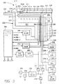
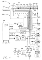


Classifications
-
- H—ELECTRICITY
- H01—ELECTRIC ELEMENTS
- H01J—ELECTRIC DISCHARGE TUBES OR DISCHARGE LAMPS
- H01J37/00—Discharge tubes with provision for introducing objects or material to be exposed to the discharge, e.g. for the purpose of examination or processing thereof
- H01J37/32—Gas-filled discharge tubes
- H01J37/32431—Constructional details of the reactor
- H01J37/32623—Mechanical discharge control means
- H01J37/32642—Focus rings
-
- H—ELECTRICITY
- H01—ELECTRIC ELEMENTS
- H01J—ELECTRIC DISCHARGE TUBES OR DISCHARGE LAMPS
- H01J37/00—Discharge tubes with provision for introducing objects or material to be exposed to the discharge, e.g. for the purpose of examination or processing thereof
- H01J37/32—Gas-filled discharge tubes
- H01J37/32009—Arrangements for generation of plasma specially adapted for examination or treatment of objects, e.g. plasma sources
- H01J37/32082—Radio frequency generated discharge
- H01J37/32174—Circuits specially adapted for controlling the RF discharge
-
- H—ELECTRICITY
- H01—ELECTRIC ELEMENTS
- H01J—ELECTRIC DISCHARGE TUBES OR DISCHARGE LAMPS
- H01J37/00—Discharge tubes with provision for introducing objects or material to be exposed to the discharge, e.g. for the purpose of examination or processing thereof
- H01J37/32—Gas-filled discharge tubes
- H01J37/32431—Constructional details of the reactor
- H01J37/32623—Mechanical discharge control means
-
- H—ELECTRICITY
- H10—SEMICONDUCTOR DEVICES; ELECTRIC SOLID-STATE DEVICES NOT OTHERWISE PROVIDED FOR
- H10P—GENERIC PROCESSES OR APPARATUS FOR THE MANUFACTURE OR TREATMENT OF DEVICES COVERED BY CLASS H10
- H10P72/00—Handling or holding of wafers, substrates or devices during manufacture or treatment thereof
- H10P72/70—Handling or holding of wafers, substrates or devices during manufacture or treatment thereof for supporting or gripping
- H10P72/72—Handling or holding of wafers, substrates or devices during manufacture or treatment thereof for supporting or gripping using electrostatic chucks
- H10P72/722—Details of electrostatic chucks
-
- H—ELECTRICITY
- H01—ELECTRIC ELEMENTS
- H01J—ELECTRIC DISCHARGE TUBES OR DISCHARGE LAMPS
- H01J2237/00—Discharge tubes exposing object to beam, e.g. for analysis treatment, etching, imaging
- H01J2237/20—Positioning, supporting, modifying or maintaining the physical state of objects being observed or treated
- H01J2237/2001—Maintaining constant desired temperature
Landscapes
- Physics & Mathematics (AREA)
- Engineering & Computer Science (AREA)
- Plasma & Fusion (AREA)
- Chemical & Material Sciences (AREA)
- Analytical Chemistry (AREA)
- Drying Of Semiconductors (AREA)
- Plasma Technology (AREA)
- Chemical Vapour Deposition (AREA)
Applications Claiming Priority (3)
| Application Number | Priority Date | Filing Date | Title |
|---|---|---|---|
| US12/178,032 US20100018648A1 (en) | 2008-07-23 | 2008-07-23 | Workpiece support for a plasma reactor with controlled apportionment of rf power to a process kit ring |
| US12/178,032 | 2008-07-23 | ||
| PCT/US2009/050403 WO2010011521A2 (en) | 2008-07-23 | 2009-07-13 | Workpiece support for a plasma reactor with controlled apportionment of rf power to a process kit ring |
Publications (3)
| Publication Number | Publication Date |
|---|---|
| JP2011529273A JP2011529273A (ja) | 2011-12-01 |
| JP2011529273A5 JP2011529273A5 (enExample) | 2012-08-30 |
| JP5898955B2 true JP5898955B2 (ja) | 2016-04-06 |
Family
ID=41567570
Family Applications (1)
| Application Number | Title | Priority Date | Filing Date |
|---|---|---|---|
| JP2011520089A Active JP5898955B2 (ja) | 2008-07-23 | 2009-07-13 | プロセスキットリングへの制御されたrf電力配分を有するプラズマリアクタ用ワークピースサポート |
Country Status (7)
| Country | Link |
|---|---|
| US (1) | US20100018648A1 (enExample) |
| JP (1) | JP5898955B2 (enExample) |
| KR (1) | KR101481377B1 (enExample) |
| CN (1) | CN102106191B (enExample) |
| SG (1) | SG192540A1 (enExample) |
| TW (1) | TWI494028B (enExample) |
| WO (1) | WO2010011521A2 (enExample) |
Families Citing this family (167)
| Publication number | Priority date | Publication date | Assignee | Title |
|---|---|---|---|---|
| US8734664B2 (en) | 2008-07-23 | 2014-05-27 | Applied Materials, Inc. | Method of differential counter electrode tuning in an RF plasma reactor |
| US20140069584A1 (en) * | 2008-07-23 | 2014-03-13 | Applied Materials, Inc. | Differential counter electrode tuning in a plasma reactor with an rf-driven ceiling electrode |
| US7977123B2 (en) * | 2009-05-22 | 2011-07-12 | Lam Research Corporation | Arrangements and methods for improving bevel etch repeatability among substrates |
| US9299539B2 (en) * | 2009-08-21 | 2016-03-29 | Lam Research Corporation | Method and apparatus for measuring wafer bias potential |
| CN103081088B (zh) * | 2010-08-06 | 2016-04-06 | 应用材料公司 | 静电夹盘和使用静电夹盘的方法 |
| US9123762B2 (en) | 2010-10-22 | 2015-09-01 | Applied Materials, Inc. | Substrate support with symmetrical feed structure |
| JP5642531B2 (ja) * | 2010-12-22 | 2014-12-17 | 東京エレクトロン株式会社 | 基板処理装置及び基板処理方法 |
| KR101196422B1 (ko) * | 2011-02-22 | 2012-11-01 | 엘아이지에이디피 주식회사 | 플라즈마 처리장치 |
| JP6085079B2 (ja) * | 2011-03-28 | 2017-02-22 | 東京エレクトロン株式会社 | パターン形成方法、処理容器内の部材の温度制御方法、及び基板処理システム |
| US9966236B2 (en) * | 2011-06-15 | 2018-05-08 | Lam Research Corporation | Powered grid for plasma chamber |
| US9117867B2 (en) * | 2011-07-01 | 2015-08-25 | Applied Materials, Inc. | Electrostatic chuck assembly |
| US10224182B2 (en) * | 2011-10-17 | 2019-03-05 | Novellus Systems, Inc. | Mechanical suppression of parasitic plasma in substrate processing chamber |
| US10586686B2 (en) | 2011-11-22 | 2020-03-10 | Law Research Corporation | Peripheral RF feed and symmetric RF return for symmetric RF delivery |
| US9396908B2 (en) | 2011-11-22 | 2016-07-19 | Lam Research Corporation | Systems and methods for controlling a plasma edge region |
| JP5905735B2 (ja) * | 2012-02-21 | 2016-04-20 | 東京エレクトロン株式会社 | 基板処理装置、基板処理方法及び基板温度の設定可能帯域の変更方法 |
| US10157729B2 (en) | 2012-02-22 | 2018-12-18 | Lam Research Corporation | Soft pulsing |
| US9070536B2 (en) * | 2012-04-24 | 2015-06-30 | Applied Materials, Inc. | Plasma reactor electrostatic chuck with cooled process ring and heated workpiece support surface |
| US9412579B2 (en) * | 2012-04-26 | 2016-08-09 | Applied Materials, Inc. | Methods and apparatus for controlling substrate uniformity |
| US9948214B2 (en) * | 2012-04-26 | 2018-04-17 | Applied Materials, Inc. | High temperature electrostatic chuck with real-time heat zone regulating capability |
| US9132436B2 (en) | 2012-09-21 | 2015-09-15 | Applied Materials, Inc. | Chemical control features in wafer process equipment |
| JP6120527B2 (ja) * | 2012-11-05 | 2017-04-26 | 東京エレクトロン株式会社 | プラズマ処理方法 |
| CN103887136B (zh) * | 2012-12-20 | 2016-03-09 | 上海华虹宏力半导体制造有限公司 | 一种适用于金属干法刻蚀半导体设备的刻蚀腔室 |
| JP6080571B2 (ja) * | 2013-01-31 | 2017-02-15 | 東京エレクトロン株式会社 | 載置台及びプラズマ処理装置 |
| US10256079B2 (en) | 2013-02-08 | 2019-04-09 | Applied Materials, Inc. | Semiconductor processing systems having multiple plasma configurations |
| WO2014149258A1 (en) * | 2013-03-15 | 2014-09-25 | Applied Materials, Inc. | Apparatus and method for tuning a plasma profile using a tuning electrode in a processing chamber |
| US10032608B2 (en) | 2013-03-27 | 2018-07-24 | Applied Materials, Inc. | Apparatus and method for tuning electrode impedance for high frequency radio frequency and terminating low frequency radio frequency to ground |
| US10125422B2 (en) * | 2013-03-27 | 2018-11-13 | Applied Materials, Inc. | High impedance RF filter for heater with impedance tuning device |
| CN104217914B (zh) * | 2013-05-31 | 2016-12-28 | 中微半导体设备(上海)有限公司 | 等离子体处理装置 |
| US9460894B2 (en) * | 2013-06-28 | 2016-10-04 | Lam Research Corporation | Controlling ion energy within a plasma chamber |
| CN104347338A (zh) * | 2013-08-01 | 2015-02-11 | 中微半导体设备(上海)有限公司 | 等离子体处理装置的冷却液处理系统及方法 |
| US9754765B2 (en) * | 2013-09-30 | 2017-09-05 | Applied Materials, Inc. | Electrodes for etch |
| JP2015162266A (ja) * | 2014-02-26 | 2015-09-07 | 株式会社日立ハイテクノロジーズ | プラズマ処理装置 |
| US9472410B2 (en) * | 2014-03-05 | 2016-10-18 | Applied Materials, Inc. | Pixelated capacitance controlled ESC |
| CN103887138B (zh) * | 2014-03-31 | 2017-01-18 | 上海华力微电子有限公司 | 一种刻蚀设备的边缘环 |
| KR102302723B1 (ko) | 2014-07-23 | 2021-09-14 | 어플라이드 머티어리얼스, 인코포레이티드 | 튜닝가능한 온도 제어되는 기판 지지 어셈블리 |
| JP2016046357A (ja) * | 2014-08-22 | 2016-04-04 | 株式会社日立ハイテクノロジーズ | プラズマ処理装置 |
| JP6820832B2 (ja) * | 2014-09-04 | 2021-01-27 | コメット アーゲー | Rf電力アプリケーションのための可変電力用コンデンサ |
| US9873180B2 (en) | 2014-10-17 | 2018-01-23 | Applied Materials, Inc. | CMP pad construction with composite material properties using additive manufacturing processes |
| US9966240B2 (en) | 2014-10-14 | 2018-05-08 | Applied Materials, Inc. | Systems and methods for internal surface conditioning assessment in plasma processing equipment |
| US9355922B2 (en) | 2014-10-14 | 2016-05-31 | Applied Materials, Inc. | Systems and methods for internal surface conditioning in plasma processing equipment |
| US10875153B2 (en) | 2014-10-17 | 2020-12-29 | Applied Materials, Inc. | Advanced polishing pad materials and formulations |
| US9776361B2 (en) | 2014-10-17 | 2017-10-03 | Applied Materials, Inc. | Polishing articles and integrated system and methods for manufacturing chemical mechanical polishing articles |
| US11745302B2 (en) | 2014-10-17 | 2023-09-05 | Applied Materials, Inc. | Methods and precursor formulations for forming advanced polishing pads by use of an additive manufacturing process |
| WO2016060712A1 (en) | 2014-10-17 | 2016-04-21 | Applied Materials, Inc. | Cmp pad construction with composite material properties using additive manufacturing processes |
| US11637002B2 (en) | 2014-11-26 | 2023-04-25 | Applied Materials, Inc. | Methods and systems to enhance process uniformity |
| US9865437B2 (en) * | 2014-12-30 | 2018-01-09 | Applied Materials, Inc. | High conductance process kit |
| US20160225652A1 (en) * | 2015-02-03 | 2016-08-04 | Applied Materials, Inc. | Low temperature chuck for plasma processing systems |
| JP6539113B2 (ja) * | 2015-05-28 | 2019-07-03 | 株式会社日立ハイテクノロジーズ | プラズマ処理装置およびプラズマ処理方法 |
| US10153139B2 (en) * | 2015-06-17 | 2018-12-11 | Applied Materials, Inc. | Multiple electrode substrate support assembly and phase control system |
| US10163610B2 (en) * | 2015-07-13 | 2018-12-25 | Lam Research Corporation | Extreme edge sheath and wafer profile tuning through edge-localized ion trajectory control and plasma operation |
| US9673025B2 (en) * | 2015-07-27 | 2017-06-06 | Lam Research Corporation | Electrostatic chuck including embedded faraday cage for RF delivery and associated methods for operation, monitoring, and control |
| US9691645B2 (en) | 2015-08-06 | 2017-06-27 | Applied Materials, Inc. | Bolted wafer chuck thermal management systems and methods for wafer processing systems |
| US9741593B2 (en) | 2015-08-06 | 2017-08-22 | Applied Materials, Inc. | Thermal management systems and methods for wafer processing systems |
| US10504700B2 (en) | 2015-08-27 | 2019-12-10 | Applied Materials, Inc. | Plasma etching systems and methods with secondary plasma injection |
| US10879041B2 (en) | 2015-09-04 | 2020-12-29 | Applied Materials, Inc. | Method and apparatus of achieving high input impedance without using ferrite materials for RF filter applications in plasma chambers |
| US10593574B2 (en) | 2015-11-06 | 2020-03-17 | Applied Materials, Inc. | Techniques for combining CMP process tracking data with 3D printed CMP consumables |
| WO2017100136A1 (en) * | 2015-12-07 | 2017-06-15 | Applied Materials, Inc. | Method and apparatus for clamping and declamping substrates using electrostatic chucks |
| US10391605B2 (en) | 2016-01-19 | 2019-08-27 | Applied Materials, Inc. | Method and apparatus for forming porous advanced polishing pads using an additive manufacturing process |
| US10685862B2 (en) | 2016-01-22 | 2020-06-16 | Applied Materials, Inc. | Controlling the RF amplitude of an edge ring of a capacitively coupled plasma process device |
| US11837479B2 (en) * | 2016-05-05 | 2023-12-05 | Applied Materials, Inc. | Advanced temperature control for wafer carrier in plasma processing chamber |
| US10504754B2 (en) | 2016-05-19 | 2019-12-10 | Applied Materials, Inc. | Systems and methods for improved semiconductor etching and component protection |
| US11532497B2 (en) * | 2016-06-07 | 2022-12-20 | Applied Materials, Inc. | High power electrostatic chuck design with radio frequency coupling |
| KR101813497B1 (ko) | 2016-06-24 | 2018-01-02 | (주)제이하라 | 플라즈마 발생장치 |
| US9865484B1 (en) | 2016-06-29 | 2018-01-09 | Applied Materials, Inc. | Selective etch using material modification and RF pulsing |
| CN107768299A (zh) * | 2016-08-16 | 2018-03-06 | 北京北方华创微电子装备有限公司 | 承载装置及半导体加工设备 |
| US10629473B2 (en) | 2016-09-09 | 2020-04-21 | Applied Materials, Inc. | Footing removal for nitride spacer |
| US10665433B2 (en) * | 2016-09-19 | 2020-05-26 | Varian Semiconductor Equipment Associates, Inc. | Extreme edge uniformity control |
| US10546729B2 (en) | 2016-10-04 | 2020-01-28 | Applied Materials, Inc. | Dual-channel showerhead with improved profile |
| US10163696B2 (en) | 2016-11-11 | 2018-12-25 | Applied Materials, Inc. | Selective cobalt removal for bottom up gapfill |
| US10026621B2 (en) | 2016-11-14 | 2018-07-17 | Applied Materials, Inc. | SiN spacer profile patterning |
| JP6698502B2 (ja) * | 2016-11-21 | 2020-05-27 | 東京エレクトロン株式会社 | 載置台及びプラズマ処理装置 |
| US10431429B2 (en) | 2017-02-03 | 2019-10-01 | Applied Materials, Inc. | Systems and methods for radial and azimuthal control of plasma uniformity |
| US10395896B2 (en) * | 2017-03-03 | 2019-08-27 | Applied Materials, Inc. | Method and apparatus for ion energy distribution manipulation for plasma processing chambers that allows ion energy boosting through amplitude modulation |
| US10943834B2 (en) | 2017-03-13 | 2021-03-09 | Applied Materials, Inc. | Replacement contact process |
| WO2018194807A1 (en) * | 2017-04-21 | 2018-10-25 | Applied Materials, Inc. | Improved electrode assembly |
| US11276590B2 (en) | 2017-05-17 | 2022-03-15 | Applied Materials, Inc. | Multi-zone semiconductor substrate supports |
| US11276559B2 (en) | 2017-05-17 | 2022-03-15 | Applied Materials, Inc. | Semiconductor processing chamber for multiple precursor flow |
| JP7176860B6 (ja) | 2017-05-17 | 2022-12-16 | アプライド マテリアルズ インコーポレイテッド | 前駆体の流れを改善する半導体処理チャンバ |
| US10920320B2 (en) | 2017-06-16 | 2021-02-16 | Applied Materials, Inc. | Plasma health determination in semiconductor substrate processing reactors |
| US10727080B2 (en) | 2017-07-07 | 2020-07-28 | Applied Materials, Inc. | Tantalum-containing material removal |
| JP6865128B2 (ja) * | 2017-07-19 | 2021-04-28 | 東京エレクトロン株式会社 | プラズマ処理装置 |
| US11471999B2 (en) | 2017-07-26 | 2022-10-18 | Applied Materials, Inc. | Integrated abrasive polishing pads and manufacturing methods |
| US10297458B2 (en) | 2017-08-07 | 2019-05-21 | Applied Materials, Inc. | Process window widening using coated parts in plasma etch processes |
| US10763150B2 (en) * | 2017-09-20 | 2020-09-01 | Applied Materials, Inc. | System for coupling a voltage to spatially segmented portions of the wafer with variable voltage |
| JP6703508B2 (ja) * | 2017-09-20 | 2020-06-03 | 株式会社日立ハイテク | プラズマ処理装置及びプラズマ処理方法 |
| US10510575B2 (en) | 2017-09-20 | 2019-12-17 | Applied Materials, Inc. | Substrate support with multiple embedded electrodes |
| US10732615B2 (en) * | 2017-10-30 | 2020-08-04 | Varian Semiconductor Equipment Associates, Inc. | System and method for minimizing backside workpiece damage |
| TWI872423B (zh) * | 2017-11-17 | 2025-02-11 | 新加坡商Aes 全球公司 | 用於在空間域和時間域上控制基板上的電漿處理之系統和方法,及相關的電腦可讀取媒體 |
| US10903054B2 (en) | 2017-12-19 | 2021-01-26 | Applied Materials, Inc. | Multi-zone gas distribution systems and methods |
| US11328909B2 (en) | 2017-12-22 | 2022-05-10 | Applied Materials, Inc. | Chamber conditioning and removal processes |
| US10854426B2 (en) | 2018-01-08 | 2020-12-01 | Applied Materials, Inc. | Metal recess for semiconductor structures |
| US10679870B2 (en) | 2018-02-15 | 2020-06-09 | Applied Materials, Inc. | Semiconductor processing chamber multistage mixing apparatus |
| US10964512B2 (en) | 2018-02-15 | 2021-03-30 | Applied Materials, Inc. | Semiconductor processing chamber multistage mixing apparatus and methods |
| TWI716818B (zh) | 2018-02-28 | 2021-01-21 | 美商應用材料股份有限公司 | 形成氣隙的系統及方法 |
| US10593560B2 (en) | 2018-03-01 | 2020-03-17 | Applied Materials, Inc. | Magnetic induction plasma source for semiconductor processes and equipment |
| US10319600B1 (en) | 2018-03-12 | 2019-06-11 | Applied Materials, Inc. | Thermal silicon etch |
| US10699879B2 (en) | 2018-04-17 | 2020-06-30 | Applied Materials, Inc. | Two piece electrode assembly with gap for plasma control |
| US10886137B2 (en) | 2018-04-30 | 2021-01-05 | Applied Materials, Inc. | Selective nitride removal |
| US10555412B2 (en) | 2018-05-10 | 2020-02-04 | Applied Materials, Inc. | Method of controlling ion energy distribution using a pulse generator with a current-return output stage |
| SG11202010268QA (en) * | 2018-06-08 | 2020-12-30 | Applied Materials Inc | Apparatus for suppressing parasitic plasma in plasma enhanced chemical vapor deposition chamber |
| US10872778B2 (en) | 2018-07-06 | 2020-12-22 | Applied Materials, Inc. | Systems and methods utilizing solid-phase etchants |
| US10755941B2 (en) | 2018-07-06 | 2020-08-25 | Applied Materials, Inc. | Self-limiting selective etching systems and methods |
| US10672642B2 (en) | 2018-07-24 | 2020-06-02 | Applied Materials, Inc. | Systems and methods for pedestal configuration |
| US11183368B2 (en) | 2018-08-02 | 2021-11-23 | Lam Research Corporation | RF tuning systems including tuning circuits having impedances for setting and adjusting parameters of electrodes in electrostatic chucks |
| WO2020036801A1 (en) | 2018-08-17 | 2020-02-20 | Lam Research Corporation | Rf power compensation to reduce deposition or etch rate changes in response to substrate bulk resistivity variations |
| CN112654655A (zh) | 2018-09-04 | 2021-04-13 | 应用材料公司 | 先进抛光垫配方 |
| US11049755B2 (en) * | 2018-09-14 | 2021-06-29 | Applied Materials, Inc. | Semiconductor substrate supports with embedded RF shield |
| US10892198B2 (en) | 2018-09-14 | 2021-01-12 | Applied Materials, Inc. | Systems and methods for improved performance in semiconductor processing |
| US11062887B2 (en) | 2018-09-17 | 2021-07-13 | Applied Materials, Inc. | High temperature RF heater pedestals |
| US11417534B2 (en) | 2018-09-21 | 2022-08-16 | Applied Materials, Inc. | Selective material removal |
| US11682560B2 (en) | 2018-10-11 | 2023-06-20 | Applied Materials, Inc. | Systems and methods for hafnium-containing film removal |
| US11121002B2 (en) | 2018-10-24 | 2021-09-14 | Applied Materials, Inc. | Systems and methods for etching metals and metal derivatives |
| US11476145B2 (en) | 2018-11-20 | 2022-10-18 | Applied Materials, Inc. | Automatic ESC bias compensation when using pulsed DC bias |
| US11437242B2 (en) | 2018-11-27 | 2022-09-06 | Applied Materials, Inc. | Selective removal of silicon-containing materials |
| JP7541005B2 (ja) * | 2018-12-03 | 2024-08-27 | アプライド マテリアルズ インコーポレイテッド | チャックとアーク放電に関する性能が改良された静電チャック設計 |
| US11562890B2 (en) * | 2018-12-06 | 2023-01-24 | Applied Materials, Inc. | Corrosion resistant ground shield of processing chamber |
| US11640917B2 (en) | 2018-12-07 | 2023-05-02 | Applied Materials, Inc. | Ground electrode formed in an electrostatic chuck for a plasma processing chamber |
| US11562887B2 (en) * | 2018-12-10 | 2023-01-24 | Tokyo Electron Limited | Plasma processing apparatus and etching method |
| JP7349329B2 (ja) * | 2018-12-10 | 2023-09-22 | 東京エレクトロン株式会社 | プラズマ処理装置及びエッチング方法 |
| US11721527B2 (en) | 2019-01-07 | 2023-08-08 | Applied Materials, Inc. | Processing chamber mixing systems |
| US10920319B2 (en) | 2019-01-11 | 2021-02-16 | Applied Materials, Inc. | Ceramic showerheads with conductive electrodes |
| KR20250100790A (ko) | 2019-01-22 | 2025-07-03 | 어플라이드 머티어리얼스, 인코포레이티드 | 펄스 전압 파형을 제어하기 위한 피드백 루프 |
| US11508554B2 (en) | 2019-01-24 | 2022-11-22 | Applied Materials, Inc. | High voltage filter assembly |
| US10784089B2 (en) | 2019-02-01 | 2020-09-22 | Applied Materials, Inc. | Temperature and bias control of edge ring |
| US11367645B2 (en) | 2019-03-13 | 2022-06-21 | Applied Materials, Inc. | Temperature tunable multi-zone electrostatic chuck |
| JP7271330B2 (ja) * | 2019-06-18 | 2023-05-11 | 東京エレクトロン株式会社 | 載置台及びプラズマ処理装置 |
| KR102214333B1 (ko) | 2019-06-27 | 2021-02-10 | 세메스 주식회사 | 기판 처리 장치 및 기판 처리 방법 |
| US11894255B2 (en) * | 2019-07-30 | 2024-02-06 | Applied Materials, Inc. | Sheath and temperature control of process kit |
| JP7370228B2 (ja) * | 2019-11-22 | 2023-10-27 | 東京エレクトロン株式会社 | プラズマ処理装置 |
| US11646183B2 (en) * | 2020-03-20 | 2023-05-09 | Applied Materials, Inc. | Substrate support assembly with arc resistant coolant conduit |
| JP7450427B2 (ja) | 2020-03-25 | 2024-03-15 | 東京エレクトロン株式会社 | 基板支持器及びプラズマ処理装置 |
| JP7442365B2 (ja) * | 2020-03-27 | 2024-03-04 | 東京エレクトロン株式会社 | 基板処理装置、基板処理システム、基板処理装置の制御方法および基板処理システムの制御方法 |
| US11450546B2 (en) * | 2020-04-09 | 2022-09-20 | Applied Materials, Inc. | Semiconductor substrate support with internal channels |
| KR102890592B1 (ko) * | 2020-06-26 | 2025-11-26 | 도쿄엘렉트론가부시키가이샤 | 플라즈마 처리 장치 |
| US11615966B2 (en) | 2020-07-19 | 2023-03-28 | Applied Materials, Inc. | Flowable film formation and treatments |
| US11848176B2 (en) | 2020-07-31 | 2023-12-19 | Applied Materials, Inc. | Plasma processing using pulsed-voltage and radio-frequency power |
| US11887811B2 (en) | 2020-09-08 | 2024-01-30 | Applied Materials, Inc. | Semiconductor processing chambers for deposition and etch |
| US11699571B2 (en) | 2020-09-08 | 2023-07-11 | Applied Materials, Inc. | Semiconductor processing chambers for deposition and etch |
| US12142459B2 (en) | 2020-09-08 | 2024-11-12 | Applied Materials, Inc. | Single chamber flowable film formation and treatments |
| US11901157B2 (en) | 2020-11-16 | 2024-02-13 | Applied Materials, Inc. | Apparatus and methods for controlling ion energy distribution |
| US11798790B2 (en) | 2020-11-16 | 2023-10-24 | Applied Materials, Inc. | Apparatus and methods for controlling ion energy distribution |
| KR102592414B1 (ko) * | 2020-11-23 | 2023-10-20 | 세메스 주식회사 | 전극 제어 유닛을 구비하는 기판 처리 장치 |
| CN114566415A (zh) * | 2020-11-27 | 2022-05-31 | 中微半导体设备(上海)股份有限公司 | 等离子体处理装置 |
| JP7071008B2 (ja) * | 2020-12-04 | 2022-05-18 | 株式会社日立ハイテク | プラズマ処理装置およびプラズマ処理方法 |
| CN114664622B (zh) * | 2020-12-23 | 2024-07-05 | 中微半导体设备(上海)股份有限公司 | 一种等离子体处理装置及调节方法 |
| US11495470B1 (en) | 2021-04-16 | 2022-11-08 | Applied Materials, Inc. | Method of enhancing etching selectivity using a pulsed plasma |
| US11791138B2 (en) | 2021-05-12 | 2023-10-17 | Applied Materials, Inc. | Automatic electrostatic chuck bias compensation during plasma processing |
| US11948780B2 (en) | 2021-05-12 | 2024-04-02 | Applied Materials, Inc. | Automatic electrostatic chuck bias compensation during plasma processing |
| US11967483B2 (en) | 2021-06-02 | 2024-04-23 | Applied Materials, Inc. | Plasma excitation with ion energy control |
| US12394596B2 (en) | 2021-06-09 | 2025-08-19 | Applied Materials, Inc. | Plasma uniformity control in pulsed DC plasma chamber |
| US12525441B2 (en) | 2021-06-09 | 2026-01-13 | Applied Materials, Inc. | Plasma chamber and chamber component cleaning methods |
| US20220399186A1 (en) | 2021-06-09 | 2022-12-15 | Applied Materials, Inc. | Method and apparatus to reduce feature charging in plasma processing chamber |
| US11810760B2 (en) | 2021-06-16 | 2023-11-07 | Applied Materials, Inc. | Apparatus and method of ion current compensation |
| US11569066B2 (en) | 2021-06-23 | 2023-01-31 | Applied Materials, Inc. | Pulsed voltage source for plasma processing applications |
| US11776788B2 (en) | 2021-06-28 | 2023-10-03 | Applied Materials, Inc. | Pulsed voltage boost for substrate processing |
| US11476090B1 (en) | 2021-08-24 | 2022-10-18 | Applied Materials, Inc. | Voltage pulse time-domain multiplexing |
| US12106938B2 (en) | 2021-09-14 | 2024-10-01 | Applied Materials, Inc. | Distortion current mitigation in a radio frequency plasma processing chamber |
| US11694876B2 (en) | 2021-12-08 | 2023-07-04 | Applied Materials, Inc. | Apparatus and method for delivering a plurality of waveform signals during plasma processing |
| US11972924B2 (en) | 2022-06-08 | 2024-04-30 | Applied Materials, Inc. | Pulsed voltage source for plasma processing applications |
| US12315732B2 (en) | 2022-06-10 | 2025-05-27 | Applied Materials, Inc. | Method and apparatus for etching a semiconductor substrate in a plasma etch chamber |
| KR102757922B1 (ko) * | 2022-07-29 | 2025-01-21 | 세메스 주식회사 | 기판 지지 장치 및 이를 포함하는 기판 처리 장치 |
| US12586768B2 (en) | 2022-08-10 | 2026-03-24 | Applied Materials, Inc. | Pulsed voltage compensation for plasma processing applications |
| US12695058B2 (en) * | 2022-08-10 | 2026-07-28 | Mks Inc. | Plasma process control of multi-electrode systems equipped with ion energy sensors |
| US12272524B2 (en) | 2022-09-19 | 2025-04-08 | Applied Materials, Inc. | Wideband variable impedance load for high volume manufacturing qualification and on-site diagnostics |
| US12111341B2 (en) | 2022-10-05 | 2024-10-08 | Applied Materials, Inc. | In-situ electric field detection method and apparatus |
| JP2024166825A (ja) * | 2023-05-19 | 2024-11-29 | 東京エレクトロン株式会社 | プラズマ処理装置 |
| US12683123B2 (en) | 2023-12-11 | 2026-07-14 | Applied Materials, Inc. | Pulsed voltage waveform biasing of plasma |
Family Cites Families (27)
| Publication number | Priority date | Publication date | Assignee | Title |
|---|---|---|---|---|
| US3763031A (en) * | 1970-10-01 | 1973-10-02 | Cogar Corp | Rf sputtering apparatus |
| US5668524A (en) * | 1994-02-09 | 1997-09-16 | Kyocera Corporation | Ceramic resistor and electrostatic chuck having an aluminum nitride crystal phase |
| US5486975A (en) * | 1994-01-31 | 1996-01-23 | Applied Materials, Inc. | Corrosion resistant electrostatic chuck |
| JP3191139B2 (ja) * | 1994-12-14 | 2001-07-23 | 株式会社日立製作所 | 試料保持装置 |
| JPH11144894A (ja) * | 1997-08-29 | 1999-05-28 | Matsushita Electric Ind Co Ltd | プラズマ処理方法及び装置 |
| KR100292410B1 (ko) * | 1998-09-23 | 2001-06-01 | 윤종용 | 불순물 오염이 억제된 반도체 제조용 반응 챔버 |
| US6563076B1 (en) * | 1999-09-30 | 2003-05-13 | Lam Research Corporation | Voltage control sensor and control interface for radio frequency power regulation in a plasma reactor |
| US6521292B1 (en) * | 2000-08-04 | 2003-02-18 | Applied Materials, Inc. | Substrate support including purge ring having inner edge aligned to wafer edge |
| TW506234B (en) * | 2000-09-18 | 2002-10-11 | Tokyo Electron Ltd | Tunable focus ring for plasma processing |
| US6630201B2 (en) * | 2001-04-05 | 2003-10-07 | Angstron Systems, Inc. | Adsorption process for atomic layer deposition |
| JP4819244B2 (ja) * | 2001-05-15 | 2011-11-24 | 東京エレクトロン株式会社 | プラズマ処理装置 |
| JP2003258074A (ja) * | 2002-03-07 | 2003-09-12 | Hitachi High-Technologies Corp | 高周波電源及び半導体製造装置 |
| JP2004022822A (ja) * | 2002-06-17 | 2004-01-22 | Shibaura Mechatronics Corp | プラズマ処理方法および装置 |
| CN100418187C (zh) * | 2003-02-07 | 2008-09-10 | 东京毅力科创株式会社 | 等离子体处理装置、环形部件和等离子体处理方法 |
| WO2004082007A1 (ja) * | 2003-03-12 | 2004-09-23 | Tokyo Electron Limited | 半導体処理用の基板保持構造及びプラズマ処理装置 |
| JP4219734B2 (ja) * | 2003-05-19 | 2009-02-04 | 東京エレクトロン株式会社 | 基板保持機構およびプラズマ処理装置 |
| US20040261946A1 (en) * | 2003-04-24 | 2004-12-30 | Tokyo Electron Limited | Plasma processing apparatus, focus ring, and susceptor |
| JP4504061B2 (ja) * | 2004-03-29 | 2010-07-14 | 東京エレクトロン株式会社 | プラズマ処理方法 |
| WO2006050632A2 (en) * | 2004-11-12 | 2006-05-18 | Oc Oerlikon Balzers Ag | Impedance matching of a capacitively coupled rf plasma reactor suitable for large area substrates |
| US20070283891A1 (en) * | 2006-03-29 | 2007-12-13 | Nobuyuki Okayama | Table for supporting substrate, and vacuum-processing equipment |
| JP4935143B2 (ja) * | 2006-03-29 | 2012-05-23 | 東京エレクトロン株式会社 | 載置台及び真空処理装置 |
| JP5254533B2 (ja) * | 2006-03-31 | 2013-08-07 | 東京エレクトロン株式会社 | プラズマ処理装置と方法 |
| JP2008053496A (ja) * | 2006-08-25 | 2008-03-06 | Sumitomo Precision Prod Co Ltd | エッチング装置 |
| JP4992389B2 (ja) * | 2006-11-06 | 2012-08-08 | 東京エレクトロン株式会社 | 載置装置、プラズマ処理装置及びプラズマ処理方法 |
| JP4754469B2 (ja) * | 2006-12-15 | 2011-08-24 | 東京エレクトロン株式会社 | 基板載置台の製造方法 |
| JP2009187673A (ja) * | 2008-02-01 | 2009-08-20 | Nec Electronics Corp | プラズマ処理装置及び方法 |
| JP5294669B2 (ja) * | 2008-03-25 | 2013-09-18 | 東京エレクトロン株式会社 | プラズマ処理装置 |
-
2008
- 2008-07-23 US US12/178,032 patent/US20100018648A1/en not_active Abandoned
-
2009
- 2009-07-13 WO PCT/US2009/050403 patent/WO2010011521A2/en not_active Ceased
- 2009-07-13 SG SG2013055421A patent/SG192540A1/en unknown
- 2009-07-13 KR KR1020117004089A patent/KR101481377B1/ko not_active Expired - Fee Related
- 2009-07-13 CN CN200980128986.8A patent/CN102106191B/zh not_active Expired - Fee Related
- 2009-07-13 JP JP2011520089A patent/JP5898955B2/ja active Active
- 2009-07-23 TW TW098124886A patent/TWI494028B/zh not_active IP Right Cessation
Also Published As
| Publication number | Publication date |
|---|---|
| US20100018648A1 (en) | 2010-01-28 |
| KR20110041541A (ko) | 2011-04-21 |
| JP2011529273A (ja) | 2011-12-01 |
| WO2010011521A3 (en) | 2010-04-22 |
| CN102106191B (zh) | 2014-01-22 |
| SG192540A1 (en) | 2013-08-30 |
| WO2010011521A2 (en) | 2010-01-28 |
| TW201031280A (en) | 2010-08-16 |
| KR101481377B1 (ko) | 2015-01-12 |
| TWI494028B (zh) | 2015-07-21 |
| CN102106191A (zh) | 2011-06-22 |
Similar Documents
| Publication | Publication Date | Title |
|---|---|---|
| KR101481377B1 (ko) | 프로세스 키트 링으로의 rf 전력의 할당이 제어되는 플라즈마 반응기를 위한 워크피스 지지체 | |
| US8734664B2 (en) | Method of differential counter electrode tuning in an RF plasma reactor | |
| US20140034239A1 (en) | Differential counter electrode tuning in a plasma reactor with an rf-driven workpiece support electrode | |
| US20140069584A1 (en) | Differential counter electrode tuning in a plasma reactor with an rf-driven ceiling electrode | |
| TWI771541B (zh) | 具有低頻射頻功率分佈調節功能的等離子反應器 | |
| US20210296144A1 (en) | Substrate support pedestal having plasma confinement features | |
| TWI574345B (zh) | 靜電夾盤 | |
| TWI713078B (zh) | 用於控制電容耦合電漿製程設備之邊緣環的射頻振幅的基板支撐件及處理腔室 | |
| US10163610B2 (en) | Extreme edge sheath and wafer profile tuning through edge-localized ion trajectory control and plasma operation | |
| KR101083624B1 (ko) | 균일성 제어를 위한 분할형 무선 주파수 전극 장치 및 방법 | |
| US6887340B2 (en) | Etch rate uniformity | |
| US20040040664A1 (en) | Cathode pedestal for a plasma etch reactor | |
| KR102256216B1 (ko) | 플라즈마 처리 장치 및 플라즈마 제어 방법 | |
| CN104205299A (zh) | 用于控制基板均匀度的方法及设备 | |
| KR20160006239A (ko) | 진보된 rf 및 온도 균일성을 갖는 정전 척 | |
| JP2019054274A (ja) | 環状のバッフル | |
| CN104115260A (zh) | 具有冷却工艺环与加热工作件支撑表面的等离子体反应器静电夹盘 | |
| KR20200067104A (ko) | 플라즈마 처리 장치 및 플라즈마 처리 방법 | |
| JP2005520337A (ja) | プラズマ処理のための改良された基板ホルダ | |
| WO2023034436A1 (en) | Replaceable electrostatic chuck outer ring for edge arcing mitigation | |
| US20220068615A1 (en) | Stage and plasma processing apparatus | |
| US20040163595A1 (en) | Plasma processing apparatus | |
| CN114975056B (zh) | 用于清洁等离子体加工设备的聚焦环的导电构件 | |
| TW202514902A (zh) | 用於改良熱性能與漏電流穩定性之具有混成圓盤的靜電吸盤 |
Legal Events
| Date | Code | Title | Description |
|---|---|---|---|
| A521 | Request for written amendment filed |
Free format text: JAPANESE INTERMEDIATE CODE: A523 Effective date: 20120713 |
|
| A621 | Written request for application examination |
Free format text: JAPANESE INTERMEDIATE CODE: A621 Effective date: 20120713 |
|
| A977 | Report on retrieval |
Free format text: JAPANESE INTERMEDIATE CODE: A971007 Effective date: 20130725 |
|
| A131 | Notification of reasons for refusal |
Free format text: JAPANESE INTERMEDIATE CODE: A131 Effective date: 20130806 |
|
| A601 | Written request for extension of time |
Free format text: JAPANESE INTERMEDIATE CODE: A601 Effective date: 20131105 |
|
| A602 | Written permission of extension of time |
Free format text: JAPANESE INTERMEDIATE CODE: A602 Effective date: 20131112 |
|
| A601 | Written request for extension of time |
Free format text: JAPANESE INTERMEDIATE CODE: A601 Effective date: 20131206 |
|
| A602 | Written permission of extension of time |
Free format text: JAPANESE INTERMEDIATE CODE: A602 Effective date: 20131213 |
|
| A601 | Written request for extension of time |
Free format text: JAPANESE INTERMEDIATE CODE: A601 Effective date: 20140104 |
|
| A602 | Written permission of extension of time |
Free format text: JAPANESE INTERMEDIATE CODE: A602 Effective date: 20140114 |
|
| A521 | Request for written amendment filed |
Free format text: JAPANESE INTERMEDIATE CODE: A523 Effective date: 20140206 |
|
| A977 | Report on retrieval |
Free format text: JAPANESE INTERMEDIATE CODE: A971007 Effective date: 20140327 |
|
| A131 | Notification of reasons for refusal |
Free format text: JAPANESE INTERMEDIATE CODE: A131 Effective date: 20140520 |
|
| A601 | Written request for extension of time |
Free format text: JAPANESE INTERMEDIATE CODE: A601 Effective date: 20140820 |
|
| A602 | Written permission of extension of time |
Free format text: JAPANESE INTERMEDIATE CODE: A602 Effective date: 20140827 |
|
| A601 | Written request for extension of time |
Free format text: JAPANESE INTERMEDIATE CODE: A601 Effective date: 20140918 |
|
| A602 | Written permission of extension of time |
Free format text: JAPANESE INTERMEDIATE CODE: A602 Effective date: 20140926 |
|
| A601 | Written request for extension of time |
Free format text: JAPANESE INTERMEDIATE CODE: A601 Effective date: 20141016 |
|
| A602 | Written permission of extension of time |
Free format text: JAPANESE INTERMEDIATE CODE: A602 Effective date: 20141023 |
|
| A521 | Request for written amendment filed |
Free format text: JAPANESE INTERMEDIATE CODE: A523 Effective date: 20141119 |
|
| A131 | Notification of reasons for refusal |
Free format text: JAPANESE INTERMEDIATE CODE: A131 Effective date: 20150519 |
|
| A601 | Written request for extension of time |
Free format text: JAPANESE INTERMEDIATE CODE: A601 Effective date: 20150817 |
|
| A601 | Written request for extension of time |
Free format text: JAPANESE INTERMEDIATE CODE: A601 Effective date: 20150916 |
|
| A521 | Request for written amendment filed |
Free format text: JAPANESE INTERMEDIATE CODE: A523 Effective date: 20151005 |
|
| TRDD | Decision of grant or rejection written | ||
| A01 | Written decision to grant a patent or to grant a registration (utility model) |
Free format text: JAPANESE INTERMEDIATE CODE: A01 Effective date: 20160209 |
|
| A61 | First payment of annual fees (during grant procedure) |
Free format text: JAPANESE INTERMEDIATE CODE: A61 Effective date: 20160307 |
|
| R150 | Certificate of patent or registration of utility model |
Ref document number: 5898955 Country of ref document: JP Free format text: JAPANESE INTERMEDIATE CODE: R150 |
|
| R250 | Receipt of annual fees |
Free format text: JAPANESE INTERMEDIATE CODE: R250 |
|
| R250 | Receipt of annual fees |
Free format text: JAPANESE INTERMEDIATE CODE: R250 |
|
| R250 | Receipt of annual fees |
Free format text: JAPANESE INTERMEDIATE CODE: R250 |
|
| R250 | Receipt of annual fees |
Free format text: JAPANESE INTERMEDIATE CODE: R250 |
|
| R250 | Receipt of annual fees |
Free format text: JAPANESE INTERMEDIATE CODE: R250 |
|
| R250 | Receipt of annual fees |
Free format text: JAPANESE INTERMEDIATE CODE: R250 |
|
| R250 | Receipt of annual fees |
Free format text: JAPANESE INTERMEDIATE CODE: R250 |