JP5898705B2 - 静電クランプ、リソグラフィ装置、および、デバイス製造方法 - Google Patents
静電クランプ、リソグラフィ装置、および、デバイス製造方法 Download PDFInfo
- Publication number
- JP5898705B2 JP5898705B2 JP2013558344A JP2013558344A JP5898705B2 JP 5898705 B2 JP5898705 B2 JP 5898705B2 JP 2013558344 A JP2013558344 A JP 2013558344A JP 2013558344 A JP2013558344 A JP 2013558344A JP 5898705 B2 JP5898705 B2 JP 5898705B2
- Authority
- JP
- Japan
- Prior art keywords
- electrostatic clamp
- substrate
- multilayer film
- core member
- mask
- Prior art date
- Legal status (The legal status is an assumption and is not a legal conclusion. Google has not performed a legal analysis and makes no representation as to the accuracy of the status listed.)
- Active
Links
Images

Classifications
-
- G—PHYSICS
- G03—PHOTOGRAPHY; CINEMATOGRAPHY; ANALOGOUS TECHNIQUES USING WAVES OTHER THAN OPTICAL WAVES; ELECTROGRAPHY; HOLOGRAPHY
- G03F—PHOTOMECHANICAL PRODUCTION OF TEXTURED OR PATTERNED SURFACES, e.g. FOR PRINTING, FOR PROCESSING OF SEMICONDUCTOR DEVICES; MATERIALS THEREFOR; ORIGINALS THEREFOR; APPARATUS SPECIALLY ADAPTED THEREFOR
- G03F7/00—Photomechanical, e.g. photolithographic, production of textured or patterned surfaces, e.g. printing surfaces; Materials therefor, e.g. comprising photoresists; Apparatus specially adapted therefor
- G03F7/70—Microphotolithographic exposure; Apparatus therefor
- G03F7/70691—Handling of masks or workpieces
- G03F7/707—Chucks, e.g. chucking or un-chucking operations or structural details
- G03F7/70708—Chucks, e.g. chucking or un-chucking operations or structural details being electrostatic; Electrostatically deformable vacuum chucks
-
- G—PHYSICS
- G03—PHOTOGRAPHY; CINEMATOGRAPHY; ANALOGOUS TECHNIQUES USING WAVES OTHER THAN OPTICAL WAVES; ELECTROGRAPHY; HOLOGRAPHY
- G03F—PHOTOMECHANICAL PRODUCTION OF TEXTURED OR PATTERNED SURFACES, e.g. FOR PRINTING, FOR PROCESSING OF SEMICONDUCTOR DEVICES; MATERIALS THEREFOR; ORIGINALS THEREFOR; APPARATUS SPECIALLY ADAPTED THEREFOR
- G03F7/00—Photomechanical, e.g. photolithographic, production of textured or patterned surfaces, e.g. printing surfaces; Materials therefor, e.g. comprising photoresists; Apparatus specially adapted therefor
- G03F7/70—Microphotolithographic exposure; Apparatus therefor
- G03F7/70691—Handling of masks or workpieces
- G03F7/707—Chucks, e.g. chucking or un-chucking operations or structural details
-
- H—ELECTRICITY
- H01—ELECTRIC ELEMENTS
- H01L—SEMICONDUCTOR DEVICES NOT COVERED BY CLASS H10
- H01L21/00—Processes or apparatus adapted for the manufacture or treatment of semiconductor or solid state devices or of parts thereof
- H01L21/67—Apparatus specially adapted for handling semiconductor or electric solid state devices during manufacture or treatment thereof; Apparatus specially adapted for handling wafers during manufacture or treatment of semiconductor or electric solid state devices or components ; Apparatus not specifically provided for elsewhere
- H01L21/683—Apparatus specially adapted for handling semiconductor or electric solid state devices during manufacture or treatment thereof; Apparatus specially adapted for handling wafers during manufacture or treatment of semiconductor or electric solid state devices or components ; Apparatus not specifically provided for elsewhere for supporting or gripping
- H01L21/6831—Apparatus specially adapted for handling semiconductor or electric solid state devices during manufacture or treatment thereof; Apparatus specially adapted for handling wafers during manufacture or treatment of semiconductor or electric solid state devices or components ; Apparatus not specifically provided for elsewhere for supporting or gripping using electrostatic chucks
-
- H10P72/72—
Landscapes
- Physics & Mathematics (AREA)
- General Physics & Mathematics (AREA)
- Engineering & Computer Science (AREA)
- Condensed Matter Physics & Semiconductors (AREA)
- Manufacturing & Machinery (AREA)
- Computer Hardware Design (AREA)
- Microelectronics & Electronic Packaging (AREA)
- Power Engineering (AREA)
- Exposure And Positioning Against Photoresist Photosensitive Materials (AREA)
- Container, Conveyance, Adherence, Positioning, Of Wafer (AREA)
- Exposure Of Semiconductors, Excluding Electron Or Ion Beam Exposure (AREA)
Description
本出願は、参照により全体が本明細書に組み込まれる2011年3月17日に出願の米国特許仮出願第61/453,719号の利益を主張し、さらに、参照により全体が本明細書に組み込まれる2011年5月27日に出願の米国特許仮出願第61/490,682号の利益を主張する。
PCT国際公開公報第2011/001978号および欧州特許出願公開第1,909,308号には、請求項1の特徴部以前に記載されたような静電クランプを開示している。
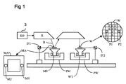
放射ビームBは、サポート構造(例えば、マスクテーブル)MT上に保持されているパターニングデバイス(例えば、マスク)MA上に入射して、パターニングデバイスによってパターン形成される。パターニングデバイス(例えば、マスク)MAから反射された後、放射ビームBは投影システムPSを通過し、投影システムPSは、基板Wのターゲット部分C上にビームの焦点をあわせる。第2ポジショナPWおよび位置センサIF2(例えば、干渉計デバイス、リニアエンコーダ、または静電容量センサ)を使って、例えば、さまざまなターゲット部分Cを放射ビームBの経路内に位置決めするように、基板テーブルWTを正確に動かすことができる。同様に、第1ポジショナPMおよび別の位置センサIF1を使い、パターニングデバイス(例えば、マスク)MAを放射ビームBの経路に対して正確に位置決めすることもできる。パターニングデバイス(例えば、マスク)MAおよび基板Wは、マスクアライメントマークM1およびM2と、基板アライメントマークP1およびP2とを使って、位置合わせされてもよい。
1.ステップモードにおいては、サポート構造(例えば、マスクテーブル)MTおよび基板テーブルWTを基本的に静止状態に保ちつつ、放射ビームに付けられたパターン全体を一度にターゲット部分C上に投影する(すなわち、単一静的露光)。その後、基板テーブルWTは、Xおよび/またはY方向に移動され、それによって別のターゲット部分Cを露光することができる。
2.スキャンモードにおいては、サポート構造(例えば、マスクテーブル)MTおよび基板テーブルWTを同期的にスキャンする一方で、放射ビームに付けられたパターンをターゲット部分C上に投影する(すなわち、単一動的露光)。サポート構造(例えば、マスクテーブル)MTに対する基板テーブルWTの速度および方向は、投影システムPSの(縮小)拡大率および像反転特性によって決めることができる。
3.別のモードにおいては、プログラマブルパターニングデバイスを保持した状態で、サポート構造(例えば、マスクテーブ)MTを基本的に静止状態に保ち、また基板テーブルWTを動かす、またはスキャンする一方で、放射ビームに付けられているパターンをターゲット部分C上に投影する。このモードにおいては、通常、パルス放射源が採用されており、さらにプログラマブルパターニングデバイスは、基板テーブルWTの移動後ごとに、またはスキャン中の連続する放射パルスと放射パルスとの間に、必要に応じて更新される。この動作モードは、前述の型のプログラマブルミラーアレイといったプログラマブルパターニングデバイスを利用するマスクレスリソグラフィに容易に適用することができる。
Claims (15)
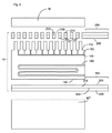
- 物体を支持テーブル上に保持する際に使用するための静電クランプであって、
複数の電気絶縁層間に位置付けられる導電層内に画成される電極を備えた多層膜と、
電位差の印加により前記多層膜を保持可能なコア部材と、を備え、
前記コア部材は複数の突起を有する表面を備え、前記多層膜は複数の貫通孔を備え、該貫通孔を貫通する前記突起を有する前記表面上に前記多層膜を位置付け可能にすることを特徴とする、
静電クランプ。 - 前記絶縁層は、ポリマー材料またはプラスチック材料から作られる、請求項1に記載の静電クランプ。
- 前記絶縁層は、ポリイミドから作られる、請求項2に記載の静電クランプ。
- 前記電気絶縁層は、ヤング率が10GPa以下の材料から形成される、請求項1〜3のいずれかに記載の静電クランプ。
- 前記膜は、150μm以下の厚さを有する、請求項1〜4のいずれかに記載の静電クランプ。
- 前記多層膜は、前記電極を、前記クランプから遠位の電圧源に電気的に接続するための電気接続を備えた伸長部分を備え、前記電気接続は、前記導電層の一体部分であり、かつ前記絶縁層の一体部分である絶縁体によって電気的に絶縁されている、請求項1〜5のいずれかに記載の静電クランプ。
- 前記導電層は、スパッタリング層であり、かつ/または前記電気絶縁層の少なくとも一層は、スピンコート層である、請求項1〜6のいずれかに記載の静電クランプ。
- 前記コア部材は、導電性部材であり、前記電極と前記コア部材との間に電位差を印加することにより、前記コア部材と前記電極との間に静電吸引力が生じる、請求項1〜7のいずれかに記載の静電クランプ。
- 前記コア部材内には、熱調整液体を通過させるためのチャネルが画成される、請求項1〜8のいずれかに記載の静電クランプ。
- 前記コア部材内には、前記物体と前記多層膜との間に向けてガスを通過させるための複数のチャネルが画成されている、請求項1〜9のいずれかに記載の静電クランプ。
- 複数の電気絶縁層間の導電層内に画成された電極を備えたさらなる多層膜をさらに備える、請求項1〜10のいずれかに記載の静電クランプ。
- 物体を保持するための支持テーブルと、前記物体を前記支持テーブル上に保持するための請求項1〜11のいずれかに記載の静電クランプと、を備える、リソグラフィ投影装置。
- 前記物体が基板である、請求項12に記載のリソグラフィ装置。
- 前記物体がマスクである、請求項12に記載のリソグラフィ装置。
- マスクを使用して投影ビームにパターンを付与するステップと、
前記パターン付与された投影ビームを基板上に投影するステップと、を備え、
前記マスクはマスクテーブルにより保持され、前記基板は基板テーブルにより保持され、
前記マスクおよび前記基板の少なくとも一方は、導電層内に画成された電極を備えた多層膜の電気絶縁層全体にわたって電位差を印加することにより、かつ、前記多層膜をコア部材上に保持するために電位差を印加することにより、各々のテーブルに保持され、前記導電層は、前記電気絶縁層の一面上に位置付けられ、前記導電層の他面上には別の電気絶縁層が位置付けられ、
前記コア部材は複数の突起を有する表面を備え、前記多層膜は複数の貫通孔を備え、該貫通孔を貫通する前記突起を有する前記表面上に前記多層膜を位置付け可能にすることを特徴とする、 デバイス製造方法。
Applications Claiming Priority (5)
| Application Number | Priority Date | Filing Date | Title |
|---|---|---|---|
| US201161453719P | 2011-03-17 | 2011-03-17 | |
| US61/453,719 | 2011-03-17 | ||
| US201161490682P | 2011-05-27 | 2011-05-27 | |
| US61/490,682 | 2011-05-27 | ||
| PCT/EP2012/052044 WO2012123188A1 (en) | 2011-03-17 | 2012-02-07 | Electrostatic clamp, lithographic apparatus, and device manufacturing method |
Publications (3)
| Publication Number | Publication Date |
|---|---|
| JP2014512675A JP2014512675A (ja) | 2014-05-22 |
| JP2014512675A5 JP2014512675A5 (ja) | 2015-03-26 |
| JP5898705B2 true JP5898705B2 (ja) | 2016-04-06 |
Family
ID=45562345
Family Applications (1)
| Application Number | Title | Priority Date | Filing Date |
|---|---|---|---|
| JP2013558344A Active JP5898705B2 (ja) | 2011-03-17 | 2012-02-07 | 静電クランプ、リソグラフィ装置、および、デバイス製造方法 |
Country Status (7)
| Country | Link |
|---|---|
| US (1) | US9360771B2 (ja) |
| EP (1) | EP2686736B1 (ja) |
| JP (1) | JP5898705B2 (ja) |
| KR (1) | KR101872886B1 (ja) |
| CN (1) | CN103415812B (ja) |
| TW (1) | TWI560526B (ja) |
| WO (1) | WO2012123188A1 (ja) |
Families Citing this family (3)
| Publication number | Priority date | Publication date | Assignee | Title |
|---|---|---|---|---|
| WO2016147539A1 (ja) * | 2015-03-16 | 2016-09-22 | セイコーエプソン株式会社 | 圧電素子の製造方法、圧電素子、圧電駆動装置、ロボット、およびポンプ |
| CN111771166B (zh) * | 2018-02-13 | 2023-12-05 | Asml荷兰有限公司 | 在光刻设备中的原位颗粒移除的设备和方法 |
| US11673161B2 (en) * | 2019-03-11 | 2023-06-13 | Technetics Group Llc | Methods of manufacturing electrostatic chucks |
Family Cites Families (28)
| Publication number | Priority date | Publication date | Assignee | Title |
|---|---|---|---|---|
| US4139833A (en) | 1976-11-22 | 1979-02-13 | Gould Inc. | Resistance temperature sensor |
| GB2106325A (en) * | 1981-09-14 | 1983-04-07 | Philips Electronic Associated | Electrostatic chuck |
| US5221403A (en) | 1990-07-20 | 1993-06-22 | Tokyo Electron Limited | Support table for plate-like body and processing apparatus using the table |
| JPH05166757A (ja) * | 1991-12-13 | 1993-07-02 | Tokyo Electron Ltd | 被処理体の温調装置 |
| KR100238629B1 (ko) | 1992-12-17 | 2000-01-15 | 히가시 데쓰로 | 정전척을 가지는 재치대 및 이것을 이용한 플라즈마 처리장치 |
| US5822171A (en) * | 1994-02-22 | 1998-10-13 | Applied Materials, Inc. | Electrostatic chuck with improved erosion resistance |
| US5646814A (en) * | 1994-07-15 | 1997-07-08 | Applied Materials, Inc. | Multi-electrode electrostatic chuck |
| US5671116A (en) * | 1995-03-10 | 1997-09-23 | Lam Research Corporation | Multilayered electrostatic chuck and method of manufacture thereof |
| US5835333A (en) | 1995-10-30 | 1998-11-10 | Lam Research Corporation | Negative offset bipolar electrostatic chucks |
| US5986873A (en) * | 1996-07-01 | 1999-11-16 | Packard Hughes Interconnect Co. | Creating surface topography on an electrostatic chuck with a mandrel |
| US5835334A (en) | 1996-09-30 | 1998-11-10 | Lam Research | Variable high temperature chuck for high density plasma chemical vapor deposition |
| JP3936004B2 (ja) * | 1996-11-26 | 2007-06-27 | 財団法人神奈川科学技術アカデミー | 静電浮上チャック |
| EP0947884B1 (en) | 1998-03-31 | 2004-03-10 | ASML Netherlands B.V. | Lithographic projection apparatus with substrate holder |
| JP2000036449A (ja) * | 1998-07-17 | 2000-02-02 | Nikon Corp | 露光装置 |
| JP4640876B2 (ja) * | 2000-06-13 | 2011-03-02 | 株式会社アルバック | 基板搬送装置 |
| US6542224B2 (en) | 2000-10-13 | 2003-04-01 | Corning Incorporated | Silica-based light-weight EUV lithography stages |
| EP1359469B1 (en) | 2002-05-01 | 2011-03-02 | ASML Netherlands B.V. | Chuck, lithographic projection apparatus and device manufacturing method |
| US6994444B2 (en) * | 2002-06-14 | 2006-02-07 | Asml Holding N.V. | Method and apparatus for managing actinic intensity transients in a lithography mirror |
| US7092231B2 (en) * | 2002-08-23 | 2006-08-15 | Asml Netherlands B.V. | Chuck, lithographic apparatus and device manufacturing method |
| US7105836B2 (en) * | 2002-10-18 | 2006-09-12 | Asml Holding N.V. | Method and apparatus for cooling a reticle during lithographic exposure |
| JP2004247387A (ja) * | 2003-02-12 | 2004-09-02 | Sumitomo Electric Ind Ltd | 半導体製造装置用ウェハ保持体およびそれを搭載した半導体製造装置 |
| TWI431707B (zh) | 2005-07-08 | 2014-03-21 | 創意科技股份有限公司 | Electrostatic cups and electrostatic chuck with the electrode sheet |
| US7626681B2 (en) * | 2005-12-28 | 2009-12-01 | Asml Netherlands B.V. | Lithographic apparatus and method |
| US7940511B2 (en) | 2007-09-21 | 2011-05-10 | Asml Netherlands B.V. | Electrostatic clamp, lithographic apparatus and method of manufacturing an electrostatic clamp |
| NL1036460A1 (nl) | 2008-02-20 | 2009-08-24 | Asml Netherlands Bv | Lithographic apparatus and device manufacturing method. |
| JP2010161319A (ja) * | 2009-01-09 | 2010-07-22 | Nikon Corp | 静電吸着保持装置、露光装置及びデバイスの製造方法 |
| SG177448A1 (en) | 2009-07-02 | 2012-02-28 | Creative Tech Corp | Electrostatic attracting structure and fabricating method therefor |
| NL2008630A (en) * | 2011-04-27 | 2012-10-30 | Asml Netherlands Bv | Substrate holder, lithographic apparatus, device manufacturing method, and method of manufacturing a substrate holder. |
-
2012
- 2012-02-07 JP JP2013558344A patent/JP5898705B2/ja active Active
- 2012-02-07 US US14/005,686 patent/US9360771B2/en active Active
- 2012-02-07 KR KR1020137027294A patent/KR101872886B1/ko active Active
- 2012-02-07 EP EP12702285.3A patent/EP2686736B1/en active Active
- 2012-02-07 WO PCT/EP2012/052044 patent/WO2012123188A1/en not_active Ceased
- 2012-02-07 CN CN201280012836.2A patent/CN103415812B/zh active Active
- 2012-02-22 TW TW101105881A patent/TWI560526B/zh active
Also Published As
| Publication number | Publication date |
|---|---|
| KR101872886B1 (ko) | 2018-06-29 |
| KR20140030154A (ko) | 2014-03-11 |
| EP2686736B1 (en) | 2014-12-17 |
| TW201239551A (en) | 2012-10-01 |
| US9360771B2 (en) | 2016-06-07 |
| TWI560526B (en) | 2016-12-01 |
| CN103415812A (zh) | 2013-11-27 |
| CN103415812B (zh) | 2015-10-21 |
| WO2012123188A1 (en) | 2012-09-20 |
| EP2686736A1 (en) | 2014-01-22 |
| JP2014512675A (ja) | 2014-05-22 |
| US20140218711A1 (en) | 2014-08-07 |
Similar Documents
| Publication | Publication Date | Title |
|---|---|---|
| JP5524845B2 (ja) | 静電クランプ、リソグラフィ装置および静電クランプを製造する方法 | |
| JP5960154B2 (ja) | 静電クランプ、リソグラフィ装置、および静電クランプの製造方法 | |
| JP6359565B2 (ja) | 静電クランプ | |
| JP6145564B2 (ja) | リソグラフィ装置における使用のための物体ホルダ、及び、物体ホルダを製造する方法 | |
| EP2555234B1 (en) | Electrostatic clamp, lithographic apparatus and method of manufacturing an electrostatic clamp | |
| US11048175B2 (en) | Apparatus for and method cleaning a support inside a lithography apparatus | |
| US7245357B2 (en) | Lithographic apparatus and device manufacturing method | |
| JP5898705B2 (ja) | 静電クランプ、リソグラフィ装置、および、デバイス製造方法 | |
| TWI569362B (zh) | 靜電夾具 | |
| NL2007631A (en) | Electrostatic clamp, lithographic apparatus, and device manufacturing method. |
Legal Events
| Date | Code | Title | Description |
|---|---|---|---|
| A521 | Request for written amendment filed |
Free format text: JAPANESE INTERMEDIATE CODE: A523 Effective date: 20150204 |
|
| A621 | Written request for application examination |
Free format text: JAPANESE INTERMEDIATE CODE: A621 Effective date: 20150204 |
|
| A131 | Notification of reasons for refusal |
Free format text: JAPANESE INTERMEDIATE CODE: A131 Effective date: 20150924 |
|
| A521 | Request for written amendment filed |
Free format text: JAPANESE INTERMEDIATE CODE: A523 Effective date: 20151211 |
|
| TRDD | Decision of grant or rejection written | ||
| A01 | Written decision to grant a patent or to grant a registration (utility model) |
Free format text: JAPANESE INTERMEDIATE CODE: A01 Effective date: 20160225 |
|
| A61 | First payment of annual fees (during grant procedure) |
Free format text: JAPANESE INTERMEDIATE CODE: A61 Effective date: 20160304 |
|
| R150 | Certificate of patent or registration of utility model |
Ref document number: 5898705 Country of ref document: JP Free format text: JAPANESE INTERMEDIATE CODE: R150 |
|
| R250 | Receipt of annual fees |
Free format text: JAPANESE INTERMEDIATE CODE: R250 |
|
| R250 | Receipt of annual fees |
Free format text: JAPANESE INTERMEDIATE CODE: R250 |
|
| R250 | Receipt of annual fees |
Free format text: JAPANESE INTERMEDIATE CODE: R250 |
|
| R250 | Receipt of annual fees |
Free format text: JAPANESE INTERMEDIATE CODE: R250 |
|
| R250 | Receipt of annual fees |
Free format text: JAPANESE INTERMEDIATE CODE: R250 |
|
| R250 | Receipt of annual fees |
Free format text: JAPANESE INTERMEDIATE CODE: R250 |
|
| R250 | Receipt of annual fees |
Free format text: JAPANESE INTERMEDIATE CODE: R250 |