JP5898705B2 - Electrostatic clamp, lithographic apparatus, and device manufacturing method - Google Patents
Electrostatic clamp, lithographic apparatus, and device manufacturing method Download PDFInfo
- Publication number
- JP5898705B2 JP5898705B2 JP2013558344A JP2013558344A JP5898705B2 JP 5898705 B2 JP5898705 B2 JP 5898705B2 JP 2013558344 A JP2013558344 A JP 2013558344A JP 2013558344 A JP2013558344 A JP 2013558344A JP 5898705 B2 JP5898705 B2 JP 5898705B2
- Authority
- JP
- Japan
- Prior art keywords
- electrostatic clamp
- substrate
- multilayer film
- core member
- mask
- Prior art date
- Legal status (The legal status is an assumption and is not a legal conclusion. Google has not performed a legal analysis and makes no representation as to the accuracy of the status listed.)
- Active
Links
Images

Classifications
-
- G—PHYSICS
- G03—PHOTOGRAPHY; CINEMATOGRAPHY; ANALOGOUS TECHNIQUES USING WAVES OTHER THAN OPTICAL WAVES; ELECTROGRAPHY; HOLOGRAPHY
- G03F—PHOTOMECHANICAL PRODUCTION OF TEXTURED OR PATTERNED SURFACES, e.g. FOR PRINTING, FOR PROCESSING OF SEMICONDUCTOR DEVICES; MATERIALS THEREFOR; ORIGINALS THEREFOR; APPARATUS SPECIALLY ADAPTED THEREFOR
- G03F7/00—Photomechanical, e.g. photolithographic, production of textured or patterned surfaces, e.g. printing surfaces; Materials therefor, e.g. comprising photoresists; Apparatus specially adapted therefor
- G03F7/70—Microphotolithographic exposure; Apparatus therefor
- G03F7/70691—Handling of masks or workpieces
- G03F7/707—Chucks, e.g. chucking or un-chucking operations or structural details
- G03F7/70708—Chucks, e.g. chucking or un-chucking operations or structural details being electrostatic; Electrostatically deformable vacuum chucks
-
- G—PHYSICS
- G03—PHOTOGRAPHY; CINEMATOGRAPHY; ANALOGOUS TECHNIQUES USING WAVES OTHER THAN OPTICAL WAVES; ELECTROGRAPHY; HOLOGRAPHY
- G03F—PHOTOMECHANICAL PRODUCTION OF TEXTURED OR PATTERNED SURFACES, e.g. FOR PRINTING, FOR PROCESSING OF SEMICONDUCTOR DEVICES; MATERIALS THEREFOR; ORIGINALS THEREFOR; APPARATUS SPECIALLY ADAPTED THEREFOR
- G03F7/00—Photomechanical, e.g. photolithographic, production of textured or patterned surfaces, e.g. printing surfaces; Materials therefor, e.g. comprising photoresists; Apparatus specially adapted therefor
- G03F7/70—Microphotolithographic exposure; Apparatus therefor
- G03F7/70691—Handling of masks or workpieces
- G03F7/707—Chucks, e.g. chucking or un-chucking operations or structural details
-
- H—ELECTRICITY
- H10—SEMICONDUCTOR DEVICES; ELECTRIC SOLID-STATE DEVICES NOT OTHERWISE PROVIDED FOR
- H10P—GENERIC PROCESSES OR APPARATUS FOR THE MANUFACTURE OR TREATMENT OF DEVICES COVERED BY CLASS H10
- H10P72/00—Handling or holding of wafers, substrates or devices during manufacture or treatment thereof
- H10P72/70—Handling or holding of wafers, substrates or devices during manufacture or treatment thereof for supporting or gripping
- H10P72/72—Handling or holding of wafers, substrates or devices during manufacture or treatment thereof for supporting or gripping using electrostatic chucks
Landscapes
- Physics & Mathematics (AREA)
- General Physics & Mathematics (AREA)
- Exposure And Positioning Against Photoresist Photosensitive Materials (AREA)
- Container, Conveyance, Adherence, Positioning, Of Wafer (AREA)
- Exposure Of Semiconductors, Excluding Electron Or Ion Beam Exposure (AREA)
Description
[関連出願の相互参照]
本出願は、参照により全体が本明細書に組み込まれる2011年3月17日に出願の米国特許仮出願第61/453,719号の利益を主張し、さらに、参照により全体が本明細書に組み込まれる2011年5月27日に出願の米国特許仮出願第61/490,682号の利益を主張する。
[Cross-reference of related applications]
This application claims the benefit of US Provisional Application No. 61 / 453,719, filed Mar. 17, 2011, which is hereby incorporated by reference in its entirety, and is further incorporated herein by reference in its entirety. The benefit of US Provisional Application No. 61 / 490,682, filed May 27, 2011, is incorporated.
[0001] 本発明は、リソグラフィ装置、静電クランプ、および、デバイス製造方法に関する。 The present invention relates to a lithographic apparatus, an electrostatic clamp, and a device manufacturing method.
[0002] リソグラフィ装置は、所望のパターンを基板上、通常、基板のターゲット部分上に付与する機械である。リソグラフィ装置は、例えば、集積回路(IC)の製造に用いることができる。その場合、ICの個々の層上に形成される回路パターンを生成するために、マスクまたはレチクルとも呼ばれるパターニングデバイスを用いることができる。このパターンは、基板(例えば、シリコンウェーハ)上のターゲット部分(例えば、ダイの一部、または1つ以上のダイを含む)に転写することができる。通常、パターンの転写は、基板上に設けられた放射感応性材料(レジスト)層上への結像によって行われる。一般には、単一の基板が、連続的にパターニングされる隣接したターゲット部分のネットワークを含んでいる。 A lithographic apparatus is a machine that applies a desired pattern onto a substrate, usually onto a target portion of the substrate. A lithographic apparatus can be used, for example, in the manufacture of integrated circuits (ICs). In that case, a patterning device, also referred to as a mask or a reticle, may be used to generate a circuit pattern formed on an individual layer of the IC. This pattern can be transferred onto a target portion (eg including part of, one, or more dies) on a substrate (eg a silicon wafer). Usually, the pattern is transferred by imaging on a radiation-sensitive material (resist) layer provided on the substrate. In general, a single substrate will contain a network of adjacent target portions that are successively patterned.
[0003] リソグラフィは、ICおよび他のデバイスおよび/または構造の製造における重要なステップの1つとして広く認識されている。しかし、リソグラフィを使用して作られるフィーチャの寸法が小さくなるにつれ、リソグラフィは、小型のICまたは他のデバイスおよび/または構造の製造を可能にするためのより重要な要因になってきている。 [0003] Lithography is widely recognized as one of the key steps in the manufacture of ICs and other devices and / or structures. However, as the dimensions of features created using lithography become smaller, lithography has become a more important factor to enable the manufacture of small ICs or other devices and / or structures.
[0004] パターンプリンティングの限界の理論的な推測は、式(1)に示す解像度についてのレイリー基準によって与えられ得る:
![]()
![]()
[0005] 露光波長を短くするため、ひいては、最小印刷可能サイズを縮小するために、極端紫外線(EUV)放射源を使用することが提案されている。EUV放射源は、約13nmの放射波長を出力するように構成される。したがって、EUV放射源は、小さいフィーチャの印刷を実現するための重要なステップを構成し得る。そのような放射は、極端紫外線または軟x線と呼ばれ、考えられる放射源としては、例えば、レーザ生成プラズマ源、放電プラズマ源、または電子蓄積リングからのシンクロトロン放射が含まれる。EUV放射源は、有用なEUV帯域内放射と共に、ほぼ同量の(時にはより多量の)望ましくない帯域外赤外線(IR)および深紫外線(DUV)放射を生成し得る。 [0005] It has been proposed to use an extreme ultraviolet (EUV) radiation source to shorten the exposure wavelength and thus reduce the minimum printable size. The EUV radiation source is configured to output a radiation wavelength of about 13 nm. Thus, EUV radiation sources can constitute an important step for achieving small feature printing. Such radiation is termed extreme ultraviolet or soft x-ray, and possible sources include, for example, laser-produced plasma sources, discharge plasma sources, or synchrotron radiation from electron storage rings. An EUV radiation source can produce approximately the same amount (sometimes more) of unwanted out-of-band infrared (IR) and deep ultraviolet (DUV) radiation, with useful EUV in-band radiation.
[0006] リソグラフィ装置において、基板は、基板テーブル上に非常に強固に保持されるため、スキャン動作中に基板テーブルが高加速を受けている時でも、基板の位置は正確に把握することができる。既存の機械では、基板ホルダまたはチャックは、壁に囲まれたピンプル状表面を備える。基板は、この壁およびピンプル上に載置され、基板後方の空間は、上方の空気圧が基板を定位置に保持する強力なクランプ力を提供するように、真空排気される。このような基板ホルダについて、参照により本明細書に組み込まれる欧州特許出願公開第0,947,884A号にさらに詳細に記載されている。 In a lithographic apparatus, the substrate is held very firmly on the substrate table, so that the position of the substrate can be accurately grasped even when the substrate table is subjected to high acceleration during the scanning operation. . In existing machines, the substrate holder or chuck comprises a pimple-like surface surrounded by a wall. The substrate rests on this wall and pimple, and the space behind the substrate is evacuated so that the upper air pressure provides a strong clamping force that holds the substrate in place. Such a substrate holder is described in more detail in EP 0,947,884A, which is incorporated herein by reference.
[0007] 上記のタイプの基板ホルダは、今日のリソグラフィ装置には有効であることが証明されている。しかし、上述したように、より小さいサイズのフィーチャを結像するという絶えず存在する需要を満たすには、投影ビームに使用する放射の波長を短くすることが必要である。したがって、現在のデバイスが、例えば248nm、193nm、または157nmの波長を有する紫外線を使用する一方、解像度の向上には、極端紫外線(EUV)(つまり、約50nm未満の波長を有する)、X線、電子またはイオンを利用したリソグラフィ装置の開発が必要になる。これらの提案されたタイプの放射には、全てに共通して、ビームパス、あるいは少なくともその実質部分が真空内に保たれなくてはならないという条件がある。したがって、基板上方に空気圧が全くない状態では、従来の真空型の基板ホルダは機能することができない。 [0007] A substrate holder of the type described above has proven effective in today's lithographic apparatus. However, as mentioned above, to meet the ever-present demand for imaging smaller sized features, it is necessary to shorten the wavelength of radiation used for the projection beam. Thus, while current devices use ultraviolet radiation having a wavelength of, for example, 248 nm, 193 nm, or 157 nm, for improved resolution, extreme ultraviolet (EUV) (ie, having a wavelength of less than about 50 nm), X-ray, It is necessary to develop a lithography apparatus using electrons or ions. All these proposed types of radiation have the common requirement that the beam path, or at least a substantial part thereof, must be kept in a vacuum. Therefore, the conventional vacuum type substrate holder cannot function when there is no air pressure above the substrate.
[0008] 同様の条件が、マスク描画装置、マスククリーニング装置、およびマスク検査装置でも満たされなくてはなないため、チャックは、リソグラフィ装置と同じ問題を抱える。 [0008] Since similar conditions must be satisfied in the mask drawing apparatus, mask cleaning apparatus, and mask inspection apparatus, the chuck has the same problem as the lithography apparatus.
[0009] したがって、静電チャックを使用して、静電力で基板を基板テーブル上に保持することが提案されている。静電力を生じさせるために、電極により、誘電材料全体に電位差が印加される。このような静電チャック(またはクランプ) の一例では、基板上の電極と、基板テーブル内または基板テーブル上の電極との間に電位差が印加される。電位差が印加されると、基板の電極とテーブルの電極とは逆帯電し、基板を定位置にクランプするのに十分な力で互いを吸引し合う。 Therefore, it has been proposed to use an electrostatic chuck to hold a substrate on a substrate table with an electrostatic force. In order to generate an electrostatic force, an electrode applies a potential difference across the dielectric material. In one example of such an electrostatic chuck (or clamp), a potential difference is applied between an electrode on the substrate and an electrode in or on the substrate table. When a potential difference is applied, the electrode on the substrate and the electrode on the table are reversely charged and attract each other with sufficient force to clamp the substrate in place.
[0010] 米国特許出願公開第2002/0044267号には、ホルダが位置決めされるULE(商標)ガラス製の定盤を備えたホルダが開示されている。ホルダは、例えば、米国特許第5,221,403号、第5,835,333号、または第5,835,334号に開示されるような静電チャックであってよい。 US Patent Application Publication No. 2002/0044267 discloses a holder having a surface plate made of ULE ™ glass on which the holder is positioned. The holder may be, for example, an electrostatic chuck as disclosed in US Pat. Nos. 5,221,403, 5,835,333, or 5,835,334.
[0011] 欧州特許出願公開第1,359,469A1号は、所定の特性を有する誘電体を使用することを開示し、かつ、ガラスまたはガラスセラミックスを使用することを示唆している。
PCT国際公開公報第2011/001978号および欧州特許出願公開第1,909,308号には、請求項1の特徴部以前に記載されたような静電クランプを開示している。
[0011] European Patent Application Publication No. 1,359,469A1 discloses the use of a dielectric having predetermined characteristics and suggests the use of glass or glass ceramics.
PCT International Publication No. 2011/001978 and European Patent Application Publication No. 1,909,308 disclose electrostatic clamps as described before the features of claim 1.
[0012] 電極を介在させたガラスまたはガラスセラミックスまたはセラミックスのスタックを製造することは難しいため、歩留まりが低いことから高価であり、かつリードタイムも長くなる。 [0012] Since it is difficult to manufacture glass or glass ceramics or ceramic stacks with electrodes interposed therebetween, the yield is low and the cost is high, and the lead time is long.
[0013] 例えば、静電クランプの複雑性を軽減することおよび/または静電クランプの製造をより容易にすることが望ましい。 [0013] For example, it may be desirable to reduce the complexity of the electrostatic clamp and / or make the manufacture of the electrostatic clamp easier.
[0014] 本発明の一実施形態によると、物体を支持テーブル上に保持する際に使用するための静電クランプであって、複数の電気絶縁層間に位置付けられる導電層内に画成される電極を備えた多層膜と、電位差の印加により多層膜を保持可能なコア部材と、を備え、コア部材は複数の突起を有する表面を備え、前記多層膜は複数の貫通孔を備え、該貫通孔を貫通する前記突起を有する前記表面上に前記多層膜を位置付け可能にすることを特徴とする、静電クランプが提供される。 [0014] According to one embodiment of the present invention, an electrode is defined in a conductive layer positioned between a plurality of electrically insulating layers for use in holding an object on a support table. And a core member capable of holding the multilayer film by applying a potential difference. The core member includes a surface having a plurality of protrusions. The multilayer film includes a plurality of through holes. An electrostatic clamp is provided , characterized in that the multilayer film can be positioned on the surface having the protrusion penetrating it .
[0015] 本発明の一実施形態によると、マスクを使用して投影ビームにパターンを付与するステップと、パターン付与された投影ビームを基板上に投影するステップと、を備えたデバイス製造方法であって、マスクはマスクテーブルにより保持され、基板は基板テーブルにより保持され、マスクおよび基板の少なくとも一方は、導電層内に画成された電極を備えた多層膜の電気絶縁層全体にわたって電位差を印加することにより、かつ、前記多層膜をコア部材上に保持するために電位差を印加することにより、各々のテーブルに保持され、導電層は、電気絶縁層の一面上に位置付けられ、導電層の他面上には別の電気絶縁層が位置付けられ、コア部材は複数の突起を有する表面を備え、多層膜は複数の貫通孔を備え、該貫通孔を貫通する突起を有する表面上に多層膜を位置付け可能にすることを特徴とする、デバイス製造方法が提供される。 [0015] According to an embodiment of the present invention, there is provided a device manufacturing method comprising: applying a pattern to a projection beam using a mask; and projecting the patterned projection beam onto a substrate. The mask is held by the mask table, the substrate is held by the substrate table, and at least one of the mask and the substrate applies a potential difference across the electrical insulating layer of the multilayer film with the electrodes defined in the conductive layer. And by applying a potential difference to hold the multilayer film on the core member , the conductive layer is held on each table, and the conductive layer is positioned on one surface of the electrically insulating layer. Another electrical insulating layer is positioned thereon , the core member has a surface having a plurality of protrusions, the multilayer film has a plurality of through holes, and the protrusions that pass through the through holes. There is provided a device manufacturing method characterized in that a multilayer film can be positioned on a surface to be processed.
[0017] 本発明の多様な特徴および利点、ならびに本発明の多様な実施形態の構造および動作を、添付の図面を参照して以下に詳細に説明する。本発明は、本明細書に記載する特定の実施形態に限定されない。このような実施形態は、説明のみを目的として本明細書に記載するものである。本明細書に含まれる教示に基づき、さらなる実施形態が当業者には明らかになるであろう。 [0017] Various features and advantages of the present invention, as well as the structure and operation of various embodiments of the present invention, are described in detail below with reference to the accompanying drawings. The present invention is not limited to the specific embodiments described herein. Such embodiments are described herein for illustrative purposes only. Further embodiments will be apparent to those skilled in the art based on the teachings contained herein.
[0018] 本発明のいくつかの実施形態を、単なる例として、添付の概略図を参照して以下に説明する。これらの図面において同じ参照符号は対応する部分を示す。 [0018] Some embodiments of the invention will now be described, by way of example only, with reference to the accompanying schematic drawings. In these drawings, the same reference numerals indicate corresponding parts.
[0022] 本発明の特徴および利点は、これらの図面と併せて以下に記載される詳細な説明からより明らかになるであろう。図面において、同じ参照記号は、全体を通じて対応する要素を特定する。図面において、同じ参照番号は、基本的に、同一の、機能的に同様な、および/または構造的に同様な要素を示す。 [0022] The features and advantages of the present invention will become more apparent from the detailed description set forth below when taken in conjunction with the drawings, in which: In the drawings, like reference characters identify corresponding elements throughout. In the drawings, like reference numbers generally indicate identical, functionally similar, and / or structurally similar elements.
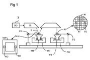
[0023] 図1は、本発明の一実施形態であり得る、あるいは本発明の一実施形態を含み得る、リソグラフィ装置の一実施形態を概略的に示している。このリソグラフィ装置は、放射ビームB(例えば、EUV放射)を調整するように構成された照明システム(イルミネータ)ILと、パターニングデバイス(例えば、マスクまたはレチクル)MAを支持するように構築され、かつパターニングデバイスを正確に位置決めするように構成された第1ポジショナPMに連結されたサポート構造またはパターニングデバイスサポート(例えば、マスクテーブル)MTと、基板(例えば、レジストコートウェーハ)Wを保持するように構築され、かつ基板を正確に位置決めするように構成された第2ポジショナPWに連結された基板テーブル(例えば、ウエーハテーブル)WTと、パターニングデバイスMAによって放射ビームBに付けられたパターンを基板Wのターゲット部分C(例えば、1つ以上のダイを含む)上に投影するように構成された投影システム(例えば、反射投影レンズシステム)PSと、を備える。 [0023] FIG. 1 schematically depicts an embodiment of a lithographic apparatus that may be an embodiment of the invention or may include an embodiment of the invention. The lithographic apparatus is constructed and patterned to support an illumination system (illuminator) IL configured to condition a radiation beam B (eg, EUV radiation) and a patterning device (eg, mask or reticle) MA. Built to hold a support structure or patterning device support (eg, mask table) MT coupled to a first positioner PM configured to accurately position the device and a substrate (eg, resist-coated wafer) W A substrate table (e.g., a wafer table) WT coupled to a second positioner PW configured to accurately position the substrate, and a pattern applied to the radiation beam B by the patterning device MA on a target portion of the substrate W C (for example, one or more Comprising a projection system configured to project onto includes a die) (e.g., a reflective projection lenses system) PS, a.
[0024] 照明システムとしては、放射を誘導し、整形し、または制御するために、屈折型、反射型、磁気型、電磁型、静電型、またはその他のタイプの光コンポーネント、あるいはそれらのあらゆる組合せなどのさまざまなタイプの光コンポーネントを含むことができる。 [0024] The illumination system may be a refractive, reflective, magnetic, electromagnetic, electrostatic, or other type of optical component, or any of them, to induce, shape, or control radiation Various types of optical components such as combinations can be included.
[0025] サポート構造MTは、パターニングデバイスの向き、リソグラフィ装置の設計、および、パターニングデバイスが真空環境内で保持されているか否かなどの他の条件に応じた態様で、パターニングデバイスMAを保持する。サポート構造は、機械式、真空式、静電式またはその他のクランプ技術を使って、パターニングデバイスを保持することができる。サポート構造は、例えば、必要に応じて固定または可動式にすることができるフレームまたはテーブルであってもよい。サポート構造は、パターニングデバイスを、例えば、投影システムに対して所望の位置に確実に置くことができる。 [0025] The support structure MT holds the patterning device MA in a manner that depends on the orientation of the patterning device, the design of the lithographic apparatus, and other conditions, such as whether or not the patterning device is held in a vacuum environment. . The support structure can hold the patterning device using mechanical, vacuum, electrostatic or other clamping techniques. The support structure may be, for example, a frame or table that can be fixed or movable as required. The support structure may ensure that the patterning device is at a desired position, for example with respect to the projection system.
[0026] 「パターニングデバイス」という用語は、基板のターゲット部分内にパターンを作り出すように、放射ビームの断面にパターンを与えるために使用できるあらゆるデバイスを指していると、広く解釈されるべきである。放射ビームに付与されたパターンは、集積回路などのターゲット部分内に作り出されるデバイス内の特定の機能層に対応することになる。 [0026] The term "patterning device" should be interpreted broadly to refer to any device that can be used to provide a pattern in a cross section of a radiation beam so as to create a pattern in a target portion of a substrate. . The pattern imparted to the radiation beam will correspond to a particular functional layer in a device being created in the target portion, such as an integrated circuit.
[0027] パターニングデバイスは、透過型であっても、反射型であってもよい。パターニングデバイスの例としては、マスク、プログラマブルミラーアレイ、およびプログラマブルLCDパネルが含まれる。マスクは、リソグラフィでは公知であり、バイナリ、レべンソン型(alternating)位相シフト、およびハーフトーン型(attenuated)位相シフトなどのマスク型、ならびに種々のハイブリッドマスク型を含む。プログラマブルミラーアレイの一例では、小型ミラーのマトリックス配列が用いられており、各小型ミラーは、入射する放射ビームを様々な方向に反射させるように、個別に傾斜させることができる。傾斜されたミラーは、ミラーマトリックスによって反射される放射ビームにパターンを付ける。 [0027] The patterning device may be transmissive or reflective. Examples of patterning devices include masks, programmable mirror arrays, and programmable LCD panels. Masks are well known in lithography and include mask types such as binary, alternating phase shift, and halftone phase shift, as well as various hybrid mask types. One example of a programmable mirror array uses a matrix array of small mirrors, and each small mirror can be individually tilted to reflect the incoming radiation beam in various directions. The tilted mirror patterns the radiation beam reflected by the mirror matrix.
[0028] 「投影システム」という用語は、使われている露光放射にとって、あるいは液浸液の使用または真空の使用といった他の要因にとって適切な、屈折型、反射型、反射屈折型、磁気型、電磁型、および静電型光学系、またはそれらのあらゆる組合せを含むあらゆる型の投影システムを包含し得る。EUV放射または電子ビーム放射では、他のガスが放射または電子を吸収し過ぎるおそれがあるため、真空を使用することが望ましい場合がある。したがって、真空壁および真空ポンプを使って、ビームパス全体に真空環境を提供してもよい。 [0028] The term "projection system" refers to refractive, reflective, catadioptric, magnetic, suitable for the exposure radiation used or for other factors such as the use of immersion liquid or vacuum. Any type of projection system can be included, including electromagnetic and electrostatic optics, or any combination thereof. For EUV radiation or electron beam radiation, it may be desirable to use a vacuum because other gases may absorb too much radiation or electrons. Thus, a vacuum wall and vacuum pump may be used to provide a vacuum environment for the entire beam path.
[0029] 本明細書に示されているとおり、リソグラフィ装置は、反射型のもの(例えば、反射型マスクを採用しているもの)である。また、リソグラフィ装置は、透過型のもの(例えば、透過型マスクを採用しているもの)であってもよい。 [0029] As shown herein, the lithographic apparatus is of a reflective type (eg employing a reflective mask). Further, the lithographic apparatus may be a transmissive type (for example, a type employing a transmissive mask).
[0030] リソグラフィ装置は、2つ(デュアルステージ)以上の基板テーブル(および/または2つ以上のマスクテーブル)を有する型のものであってもよい。そのような「マルチステージ」機械においては、追加のテーブルは並行して使うことができ、または予備工程を1つ以上のテーブル上で実行しつつ、別の1つ以上のテーブルを露光用に使うこともできる。 [0030] The lithographic apparatus may be of a type having two (dual stage) or more substrate tables (and / or two or more mask tables). In such “multi-stage” machines, additional tables can be used in parallel, or one or more tables are used for exposure while a preliminary process is performed on one or more tables. You can also.
[0031] 図1を参照すると、イルミネータILは、放射源SOから放射ビームを受ける。放射源SOは、放射システム3(つまり、放射生成ユニット3)の一部であり得る。また、放射システム3とリソグラフィ装置は、別個の構成要素であってもよい。そのような場合には、放射システム3は、リソグラフィ装置の一部を形成しているとはみなされず、また放射ビームは、放射システム3の放射源SOからイルミネータILへ、例えば、適切な誘導ミラーおよび/またはビームエキスパンダを含むビームデリバリシステムを使って送られる。その他の場合においては、放射源はリソグラフィ装置の一体部分とすることもできる。
[0031] Referring to FIG. 1, the illuminator IL receives a radiation beam from a radiation source SO. The radiation source SO may be part of the radiation system 3 (ie the radiation generation unit 3). The
[0032] 放射システム3の放射源SOは、多様に構成することができる。例えば、放射源SOは、レーザ生成プラズマ源(LPP源)、例えば、スズLPP源(このようなLPP源はそれ自体が公知である)であってもよく、あるいは、放電生成プラズマ源(DPP)であってもよい。放射源SOは、異なるタイプの放射源であってもよい。
[0032] The radiation source SO of the
[0033] イルミネータILは、放射ビームの角強度分布を調節するアジャスタを含むことができる。一般に、イルミネータの瞳面内の強度分布の少なくとも外側および/または内側半径範囲(通常、それぞれσ-outerおよびσ-innerと呼ばれる)を調節することができる。さらに、イルミネータILは、インテグレータおよびコンデンサといったさまざまな他のコンポーネントを含むことができる。イルミネータを使って放射ビームを調整すれば、放射ビームの断面に所望の均一性および強度分布をもたせることができる。 [0033] The illuminator IL may include an adjuster for adjusting the angular intensity distribution of the radiation beam. In general, at least the outer and / or inner radial extent (commonly referred to as σ-outer and σ-inner, respectively) of the intensity distribution in the illuminator pupil plane can be adjusted. In addition, the illuminator IL may include various other components such as integrators and capacitors. By adjusting the radiation beam using an illuminator, the desired uniformity and intensity distribution can be provided in the cross section of the radiation beam.
[0034]
放射ビームBは、サポート構造(例えば、マスクテーブル)MT上に保持されているパターニングデバイス(例えば、マスク)MA上に入射して、パターニングデバイスによってパターン形成される。パターニングデバイス(例えば、マスク)MAから反射された後、放射ビームBは投影システムPSを通過し、投影システムPSは、基板Wのターゲット部分C上にビームの焦点をあわせる。第2ポジショナPWおよび位置センサIF2(例えば、干渉計デバイス、リニアエンコーダ、または静電容量センサ)を使って、例えば、さまざまなターゲット部分Cを放射ビームBの経路内に位置決めするように、基板テーブルWTを正確に動かすことができる。同様に、第1ポジショナPMおよび別の位置センサIF1を使い、パターニングデバイス(例えば、マスク)MAを放射ビームBの経路に対して正確に位置決めすることもできる。パターニングデバイス(例えば、マスク)MAおよび基板Wは、マスクアライメントマークM1およびM2と、基板アライメントマークP1およびP2とを使って、位置合わせされてもよい。
[0034]
The radiation beam B is incident on the patterning device (eg, mask) MA, which is held on the support structure (eg, mask table) MT, and is patterned by the patterning device. After being reflected from the patterning device (eg mask) MA, the radiation beam B passes through the projection system PS, which focuses the beam onto the target portion C of the substrate W. The substrate table is used, for example, to position various target portions C in the path of the radiation beam B using the second positioner PW and the position sensor IF2 (eg, interferometer device, linear encoder, or capacitive sensor). The WT can be moved accurately. Similarly, the first positioner PM and another position sensor IF1 can be used to accurately position the patterning device (eg mask) MA with respect to the path of the radiation beam B. Patterning device (eg mask) MA and substrate W may be aligned using mask alignment marks M1 and M2 and substrate alignment marks P1 and P2.
[0035] 例示の装置は、以下に説明するモードのうち少なくとも1つのモードで使用できる。
1.ステップモードにおいては、サポート構造(例えば、マスクテーブル)MTおよび基板テーブルWTを基本的に静止状態に保ちつつ、放射ビームに付けられたパターン全体を一度にターゲット部分C上に投影する(すなわち、単一静的露光)。その後、基板テーブルWTは、Xおよび/またはY方向に移動され、それによって別のターゲット部分Cを露光することができる。
2.スキャンモードにおいては、サポート構造(例えば、マスクテーブル)MTおよび基板テーブルWTを同期的にスキャンする一方で、放射ビームに付けられたパターンをターゲット部分C上に投影する(すなわち、単一動的露光)。サポート構造(例えば、マスクテーブル)MTに対する基板テーブルWTの速度および方向は、投影システムPSの(縮小)拡大率および像反転特性によって決めることができる。
3.別のモードにおいては、プログラマブルパターニングデバイスを保持した状態で、サポート構造(例えば、マスクテーブ)MTを基本的に静止状態に保ち、また基板テーブルWTを動かす、またはスキャンする一方で、放射ビームに付けられているパターンをターゲット部分C上に投影する。このモードにおいては、通常、パルス放射源が採用されており、さらにプログラマブルパターニングデバイスは、基板テーブルWTの移動後ごとに、またはスキャン中の連続する放射パルスと放射パルスとの間に、必要に応じて更新される。この動作モードは、前述の型のプログラマブルミラーアレイといったプログラマブルパターニングデバイスを利用するマスクレスリソグラフィに容易に適用することができる。
[0035] The example apparatus can be used in at least one of the modes described below.
1. In step mode, the entire pattern applied to the radiation beam is projected onto the target portion C at a time (ie, a single pattern) while the support structure (eg, mask table) MT and substrate table WT are essentially stationary. One static exposure). Thereafter, the substrate table WT is moved in the X and / or Y direction so that another target portion C can be exposed.
2. In scan mode, the support structure (eg, mask table) MT and substrate table WT are scanned synchronously while a pattern imparted to the radiation beam is projected onto a target portion C (ie, a single dynamic exposure). . The speed and direction of the substrate table WT relative to the support structure (eg mask table) MT can be determined by the (reduction) magnification factor and image reversal characteristics of the projection system PS.
3. In another mode, while holding the programmable patterning device, the support structure (eg, mask table) MT is kept essentially stationary and the substrate table WT is moved or scanned while being applied to the radiation beam. The projected pattern is projected onto the target portion C. In this mode, a pulsed radiation source is typically employed, and the programmable patterning device can also be used after each movement of the substrate table WT or between successive radiation pulses during a scan as needed. Updated. This mode of operation can be readily applied to maskless lithography that utilizes programmable patterning device, such as a programmable mirror array of a type as described above.
[0036] 上述の使用モードの組合せおよび/またはバリエーション、あるいは完全に異なる使用モードもまた採用可能である。 [0036] Combinations and / or variations on the above described modes of use or entirely different modes of use may also be employed.
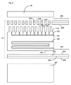
[0037] 図2は、本発明の静電クランプ10を拡大した断面図で示している。静電クランプ10は、基板Wをリソグラフィ投影装置内の基板テーブルWT上または基板ハンドラ(例えば、真空プレアライナなど)上に保持するために使用される。他の実施形態では、クランプ10は、マスクをリソグラフィ投影装置内のマスクテーブル上またはマスクハンドラ上に保持するために使用してもよい。
FIG. 2 shows an enlarged sectional view of the
[0038] 静電クランプ10は、3つの主要コンポーネント、つまり、第1膜200、コア100、および第2膜300を備える。他の設計のクランプも可能である。例えば、コア100または第2膜300を存在させずに、第1膜200を使用して基板Wを基板テーブルWTにクランプしてもよい。任意で、製造及び取扱い上の理由から、金属キャリア、例えば、金属箔または金属メッキを静電クランプの一部とすることもできる。これには、静電クランプのロバスト性が高くなるという利点がある。
The
[0039] 第1膜200および第2膜300は、多層膜である。これらの膜は、スピンコーティング、スパッタリング、スプレーコーティング、(スクリーン)印刷、化学気相蒸着(CVD)などの膜工学を使用して生成される。
[0039] The
[0040] 通常、膜200、300は可撓性であり、これは、膜が自重を支えるほどには強固ではないことを意味している。例えば、これらの膜が自重により変形可能になるように、材料のヤング率は比較的低く、層の厚さは比較的薄い。
[0040] Typically, the
[0041] 膜200、300は、典型的には、例えばスイス、レンツブルグのHIGHTEC MC AG社からHiCoFlexの商品名で入手可能なもののようなフレキシブルPCBまたは可撓性箔などの電気回路用の可撓性膜と同様の方法で作ることができる。
[0041] The
[0042] 第1および第2膜200、300は、電気絶縁層210、220、310、320の間に挟持された導電層230、330を備える。導電層230、330は、平面視で所望形状を有する1つまたは複数の電極(または導電路)を画成するように、パターン形成され得る。要求に応じて、より多くの層を使用してもよい。例えば、2層以上の導電層が絶縁層により分離され、さらに2層の外側絶縁層により挟持されている状態が、所定の状況において望ましい場合がある。
The first and
[0043] コア100は、導電性材料、例えば導電性セラミックから作ることができる。導電層230、コア100および導電層330の層間に適切な電圧を印加することにより、第1膜がコア100および基板Wに吸引され、第2膜がコア100および基板テーブルWTに吸引される。このようにして、基板Wを、基板テーブルWTに保持することができる。
[0043] The
[0044] 一実施形態において、コア100が1つ以上の電極備え、および/または、基板テーブルWTが1つ以上の電極を備え得る。しかし、基板Wおよび基板テーブルWTは、望ましい吸引力を生成するために電極を備える必要がないことが好ましい。これには、導電層230、330のそれぞれに2つ以上の電極を画成することが必要となり得る。これを実現する方法は、例えば、参照することによりその全体が本明細書に組み込まれる欧州特許出願公開第1,359,469A1号に記載されている。
[0044] In one embodiment, the
[0045] 第1および第2膜200、300の絶縁膜210、220、310、320は、ポリマー材料またはプラスチック材料から作られ得る。一実施形態において、絶縁層210、220、310、320は、ポリイミド、例えば、DuPont社からKapton(登録商標)の商品名で入手可能なポリ(4,4’−オキシジフェニレンピロメリットイミド)から作られる。
[0045] The insulating
[0046] 一実施形態において、第1膜および第2膜は、それぞれ、全厚さが150μm以下である。一実施形態では、第1膜および第2膜200、300は、それぞれ、全厚さが15μmを超える。一実施形態において、第1膜および/または第2膜200、300は、超薄可撓性膜(箔)(厚さ範囲20〜50μm)の形態を有し得る。例えば、超薄可撓性箔は、スイス、レンツブルグのHIGHTECH MC AG社から入手可能なHiCoFlex(登録商標)であり得る。このような膜は、マイクロエレクトロニクスで使用されている。この膜は、絶縁層210、220のスピンコーティングと、導電層230のスパッタリングを利用して作られる。これらのプロセスは、好ましい厚さ均一性を達成することができるが、これは、導電層230、330と吸引される部分(例えば、第1膜200に対する基板Wおよびコア100、第2膜300に対するコア100および基板テーブルWT)との間の有効ギャップのばらつきに応じて、静電力(基板Wの面積全体にわたって実質的に均一であることが望ましい)が変動し、有効ギャップは、絶縁層210、220、310、320の厚さのばらつきに応じて変動するため、重要である。HiCoFlex(登録商標)膜を使用する場合、全厚さに対する厚さ均一性は、±1.5−2μmである。
In one embodiment, the first film and the second film each have a total thickness of 150 μm or less. In one embodiment, the first film and the
[0047] 膜を構成する電気絶縁性材料の各層は、7〜8μmの厚さを有し得る。膜200、300は、2層(以上)の電気絶縁性材料(例えば、ポリイミド)の層を備え、全厚さが約15μmの電気絶縁層210、310を形成し得る。その後、導電層230がスパッタリングにより形成され、数百nmの厚さ(例えば、厚さ200nm)に成り得る。導電層230は、複数の層、例えば、TiCuTiまたはNiCrで構成され得る。スパッタリング中、マスクを使用することにより、堆積された金属にパターンを付与することができる。このようにして、導電層230内に電極が画成され得る。2層以上のさらなる電気絶縁層を導電層上に堆積して第2電気絶縁層220、320を形成し、それにより導電層を封入することができる。
[0047] Each layer of the electrically insulating material constituting the film may have a thickness of 7 to 8 μm. The
[0048] このような薄い可撓性箔は、いくつかの方法で生成することができる。例えば、プロダクト/プロセスキャリア(取り外し可/不可、厚い/薄い、可撓性/剛性)の使用、または、ウエーハテーブル(またはクランプ)上への直接的な膜生成(スピンコーティング)がある。これらの異なるケースでは、例えば、別個の可撓性膜、キャリア上の可撓性膜、またはウエーハテーブル上に一体化された可撓性膜というように、最終生成物が変わり得る。 [0048] Such thin flexible foils can be produced in several ways. For example, use of a product / process carrier (removable / impossible, thick / thin, flexible / rigid) or direct film formation (spin coating) on a wafer table (or clamp). In these different cases, the final product can vary, for example, a separate flexible membrane, a flexible membrane on a carrier, or a flexible membrane integrated on a wafer table.
[0049] 超薄可撓性箔のポリマー材料またはプラスチック材料は、ポリイミドであり得る。ポリイミドは、電極に印加される高電圧に耐性がある(ポリイミドは、漏れ止めである必要があり(例えば、ピンホール無しでは形成されない)、長期間の物理特性に優れている)。また、他の材料(または、異なる材料の組み合わせ)を絶縁層として使用してもよい。例えば、BCBまたはパリレンなどである。さらに、上述した材料の組み合わせもまた、絶縁層として使用することが可能である。例えば、ポリイミドとBCBの組み合わせを絶縁層として使用することができる。超薄可撓性膜を使用することの利点として、クランプの単純性の向上、クランプの製造容易性、および一体化した相互接続(以下参照)の形成可能性が挙げられる。つまり、可撓性膜の形成は、ガラスもしくはガラスセラミックもしくはセラミックコンポーネントを互いに接着すること、または、ガラスもしくはガラスセラミックもしくはセラミックコンポーネントを電極に接着することよりも容易である。加えて、超薄可撓性膜の製造の方が、かなり安価である。 [0049] The polymer material or plastic material of the ultra-thin flexible foil may be polyimide. Polyimides are resistant to high voltages applied to the electrodes (polyimides need to be leak-proof (eg, not formed without pinholes and have excellent long-term physical properties)). Other materials (or combinations of different materials) may be used as the insulating layer. For example, BCB or parylene. In addition, combinations of the above materials can also be used as the insulating layer. For example, a combination of polyimide and BCB can be used as the insulating layer. The advantages of using an ultra-thin flexible membrane include improved clamp simplicity, ease of manufacture of the clamp, and the possibility of forming an integrated interconnect (see below). That is, forming a flexible membrane is easier than bonding glass or glass ceramic or ceramic components to each other, or bonding glass or glass ceramic or ceramic components to an electrode. In addition, the production of ultra-thin flexible membranes is considerably less expensive.
[0050] 別の実施形態では、第1膜および/または第2膜200、300は、ベルギー、テッセンデルロのElectronic Apparatus NV社から入手可能なもののような標準的なフレキシブルPCB材料から作られてもよい。一実施形態において、このようなフレキシブルPCB材料には、PCB供給業者により使用される標準的なプロセス(例えば、ウェットエッチング加工と、それに続くホットラミネート(プレス)加工を行い、いくつかの可撓性銅クラッドを貼り合わせる/積層するプロセス)によって生成されたポリイミド、ポリエステル、PTFE、LCPのシートが含まれる。このようなフレキシブルPCB材料は、DuPont社から入手可能である。通常、フレキシブルPCBは、上面に導電層を有するKapton(登録商標)(ポリイミド、例えば、ポリ(4,4’−オキシジフェニレンピロメリットイミド))の層として供給され得る。ポリイミド層は25〜150μmの厚を有し、導電層(例えば、銅)は9〜70μmの厚さを有し得る。標準的な技法を用いて銅にパターンを付与することにより、電極を画成することができる。最終的に、カバー層(例えば、別のポリイミド層)を銅層に貼り付け、上部電気絶縁層を形成することができる。このカバー層として、全厚さが25〜125μm、典型的には約50μmの、一面に接着剤を有するKapton(登録商標)の層が市販されている。これを、パターン形成された導電層上に貼り付けることにより、電気絶縁層、接着層、導電層、および電気絶縁層を備えた多層膜を形成することができる。本実施形態では、膜200、300の全厚さは、典型的には、およそ100〜120μmになるが、60μm〜数百μmの範囲であってよい。
[0050] In another embodiment, the first membrane and / or the
[0051] 一実施形態における電気絶縁層のポリマー材料またはプラスチック材料は、ヤング率が10GPa以下、好ましくは5GPa以下である。ポリイミドは、ヤング率が約2.5GPaであり、これは、ヤング率が67GPaのULE(登録商標)に匹敵する。 [0051] The polymer material or plastic material of the electrical insulating layer in one embodiment has a Young's modulus of 10 GPa or less, preferably 5 GPa or less. Polyimide has a Young's modulus of about 2.5 GPa, which is comparable to ULE® with a Young's modulus of 67 GPa.
[0052] 図2に図示した一実施形態において、第1膜200は、使用中、コア100の上面110上に位置付けられる。第2膜300は、コア100の下面130と基板テーブルWTとの間に位置付けられる。
In the embodiment illustrated in FIG. 2, the
[0053] 一実施形態において、コア100の上面110は、複数の突起120を備え得る。第1膜200の複数の貫通孔235は、適正な位置にあるとき、平面視で突起120の位置に対応する。これにより、第1膜200を、コア100の上面110上に配置することができる。突起120は、その後、貫通孔235を貫通して突出する。突起120は、第1膜200の全厚さを超える距離分、上面110から延在するように作られる。このようにして、基板Wは、第1膜200を基板Wの下面とコア100の上面110との間に位置付けた状態で、突起120の頂部上に載置される。
[0053] In one embodiment, the
[0054] 一実施形態において、コア100の下面130上に同様の構成が使用される。つまり、コア100の下面130上には突起が存在し、第2膜300には対応する貫通孔が存在する。しかし、必ずしもこれに限られない。図2に図示したように、一実施形態において、コア100の下面130は、突起を備えず、コア100は基板テーブルWTに接触していいない。他の構成も可能である。例えば、コア100の上面110は、突起を備えず、下面130が突起を備えてもよい。別の実施形態では、下面130は突起を有するが、上面110は突起を有さない。
[0054] In one embodiment, a similar configuration is used on the
[0055] 図2に図示されるように、コア100にはチャネル140が設けられている。チャネル140は、熱調整液を通過させて提供するためのものである。このような熱調整液を使用して、コア100を一定温度に維持することができる。
As shown in FIG. 2, the
[0056] 一実施形態において、ガスを通過させて提供するためのチャネル150をコア100に設けることができる。チャネル150は、突起120と基板Wとの間にバックフィルガスを提供するためのものであり得る。第1膜200は、第1膜200と基板Wとの間の領域へとバックフィルガスを通過させることができるように孔を有し得る。このようなバックフィルガスは、基板Wと突起120との間に汚染が侵入することを防ぐことにより、清浄度を高めることができ、かつ/または、基板W上の熱分布を向上させるために使用することもできる。
[0056] In one embodiment, the
[0057] 本発明において可撓性膜を使用するさらなる利点としては、膜200、300の残りの部分と一体的な伸長部分250、350を設けることができる点が挙げられる。この伸長部分は、導電層230、330とクランプ10から遠位の電圧源との間の電気接続252(例えば、相互接続)として作用することができる。つまり、何らかの形で電極および電圧源に接続される可撓性ワイヤ(このワイヤは、基板テーブルWTがリソグラフィ装置内で移動するため、可撓性を有する必要がある)を使用する代わりに、別個のワイヤに代えて多層膜200、300の一体部分を使用することができる。
[0057] A further advantage of using a flexible membrane in the present invention is the ability to provide
[0058] 伸長部分250、330は、図3により明確に示されている。図3は、第1膜200の平面図である。伸長部分250は、任意の形状に作ることができ、クランプ10から遠位の電圧源と導電層内に画成された電極232との間に電気接続252を提供するために使用することができる。膜200の可撓性の性質により、伸長部分250は面外に湾曲し得る。
[0058] The
[0059] 導電層内には、電極232および電気接続252の両方が一体的に画成されている。電気接続252は、伸長部分250内の電気絶縁層220、210の一部により、周囲から電気的に絶縁されている。伸長部分250内の電気絶縁層220、210の一部は、電極232を絶縁する対応した電気絶縁層210、220と一体化されている。
[0059] Both
[0060] 図3に図示されるように、突起120が貫通して突出するための貫通孔235が設けられている。よりサイズの大きい追加の貫通孔245が図示されている。これらは、基板テーブルWTからコア100および第2膜300も貫通し得るピン用の貫通孔であり得る。これらのピンは、露光後、基板Wを持ち上げるために使用され得る。
As shown in FIG. 3, a through
[0061] 図3には明示されていないが、電極232は、この電極232のエッジが膜200内に完全に含まれて、貫通孔235のエッジで外部に露出しないように、貫通孔235のエッジまでは延在していなくてもよい。これは、図2において、導電層230が貫通孔235のエッジまでは延在していないという事実により示されている。
Although not explicitly shown in FIG. 3, the
[0062] 図3の膜200には、1つの電極232および1つの電気接続252のみが図示されているが、この場合に限らず、任意の数の電極232および電気接続252が存在してよい。一実施形態では、基板への電気接続の提供が必要になることを避けるために、導電層230内に2つの電極232が画成され、2つの対応する電気接続252が設けられる。
[0062] Although only one
[0063] 一実施形態において、導電路が導電層230内に画成され、かつ、反対端で電気接続252に接続されてもよい。このようにして、導電路を(電流を流すことにより)ヒータとして使用することができ、かつ/または、(例えば、抵抗の変化を検出することにより)センサとして使用することができる。その後、この膜を(例えば、接着により)リソグラフィ装置のコンポーネントの任意の表面に貼り付け、ヒータおよび/またはセンサとして使用することができる。局所ヒータおよび/または局所センサの恩恵を受け得るコンポーネントの例として、光学系のミラーの表面または他の光学要素またはチャックが挙げられる。
[0063] In one embodiment, a conductive path may be defined in the
[0064] 電極の電気接続に伸長部分250を使用することには、重量を小さくできるという利点があり、これは、より優れた動特性をもたらす。さらに、膜、特にポリマー材料またはプラスチック材料から作られた膜を使用することで、ガラスまたはガラスセラミックまたはセラミック材料を同一のコンポーネントに使用するよりも、重量が小さくなる。
[0064] The use of the
[0065] 本明細書において、IC製造におけるリソグラフィ装置の使用について具体的な言及がなされているが、本明細書記載のリソグラフィ装置が、集積光学システム、磁気ドメインメモリ用のガイダンスパターンおよび検出パターン、フラットパネルディスプレイ、液晶ディスプレイ(LCD)、薄膜磁気ヘッド等の製造といった他の用途を有し得ることが理解されるべきである。 [0065] Although specific reference is made herein to the use of a lithographic apparatus in IC manufacture, the lithographic apparatus described herein is an integrated optical system, a guidance pattern and a detection pattern for a magnetic domain memory, It should be understood that other applications such as the manufacture of flat panel displays, liquid crystal displays (LCDs), thin film magnetic heads and the like may be had.
[0066] 光リソグラフィの関連での本発明の実施形態の使用について上述のとおり具体的な言及がなされたが、当然のことながら、本発明は、他の用途、例えば、インプリントリソグラフィに使われてもよく、さらに状況が許すのであれば、光リソグラフィに限定されることはない。 [0066] Although specific reference has been made to the use of embodiments of the present invention in the context of optical lithography as described above, it will be appreciated that the present invention may be used in other applications, such as imprint lithography. However, it is not limited to optical lithography if the situation permits.
[0067] 本明細書で使用される「放射」および「ビーム」という用語は、紫外線(UV)(例えば、365nm、355nm、248nm、193nm、157nm、または126nmの波長、またはおよそこれらの値の波長を有する)、および極端紫外線(EUV)(例えば、5〜20nmの範囲の波長を有する)、ならびにイオンビームや電子ビームなどの微粒子ビームを含むあらゆる種類の電磁放射を包含している。 [0067] As used herein, the terms "radiation" and "beam" refer to ultraviolet (UV) (eg, 365 nm, 355 nm, 248 nm, 193 nm, 157 nm, or 126 nm wavelengths, or approximately the wavelength of these values). ), And extreme ultraviolet (EUV) (e.g., having a wavelength in the range of 5-20 nm), and all types of electromagnetic radiation, including particulate beams such as ion beams and electron beams.
[0068] 以上、本発明の具体的な実施形態を説明してきたが、本発明は、上述以外の態様で実施できることが明らかである。 [0068] While specific embodiments of the invention have been described above, it will be appreciated that the invention may be practiced otherwise than as described.
[0069] 上記の説明は、制限ではなく例示を意図したものである。したがって、当業者には明らかなように、添付の特許請求の範囲を逸脱することなく本記載の発明に変更を加えてもよい。 [0069] The descriptions above are intended to be illustrative, not limiting. Thus, it will be apparent to one skilled in the art that modifications may be made to the invention as described without departing from the scope of the claims set out below.
[0070] 当然のことながら、本出願において、「含む(including)」という用語は、他の要素または他のステップを排除するものではない。また、「a」および「an」という用語のそれぞれも、複数を排除するものではない。クレーム内の参照符号はいずれも、請求の範囲を限定するものと理解されるべきではない。 [0070] Of course, in this application, the term "including" does not exclude other elements or other steps. Also, the terms “a” and “an” do not exclude a plurality. Any reference signs in the claims should not be construed as limiting the claim.
Claims (15)
複数の電気絶縁層間に位置付けられる導電層内に画成される電極を備えた多層膜と、
電位差の印加により前記多層膜を保持可能なコア部材と、を備え、
前記コア部材は複数の突起を有する表面を備え、前記多層膜は複数の貫通孔を備え、該貫通孔を貫通する前記突起を有する前記表面上に前記多層膜を位置付け可能にすることを特徴とする、
静電クランプ。 An electrostatic clamp for use in holding an object on a support table,
A multilayer film comprising electrodes defined in a conductive layer positioned between a plurality of electrically insulating layers;
A core member capable of holding the multilayer film by applying a potential difference, and
The core member has a surface having a plurality of protrusions, the multilayer film has a plurality of through holes, and the multilayer film can be positioned on the surface having the protrusions passing through the through holes. To
Electrostatic clamp.
前記パターン付与された投影ビームを基板上に投影するステップと、を備え、
前記マスクはマスクテーブルにより保持され、前記基板は基板テーブルにより保持され、
前記マスクおよび前記基板の少なくとも一方は、導電層内に画成された電極を備えた多層膜の電気絶縁層全体にわたって電位差を印加することにより、かつ、前記多層膜をコア部材上に保持するために電位差を印加することにより、各々のテーブルに保持され、前記導電層は、前記電気絶縁層の一面上に位置付けられ、前記導電層の他面上には別の電気絶縁層が位置付けられ、
前記コア部材は複数の突起を有する表面を備え、前記多層膜は複数の貫通孔を備え、該貫通孔を貫通する前記突起を有する前記表面上に前記多層膜を位置付け可能にすることを特徴とする、 デバイス製造方法。
Applying a pattern to the projection beam using a mask;
Projecting the patterned projection beam onto a substrate, and
The mask is held by a mask table, the substrate is held by a substrate table;
At least one of the mask and the substrate is configured to apply a potential difference over the entire electrical insulating layer of the multilayer film including electrodes defined in the conductive layer, and to hold the multilayer film on the core member By applying a potential difference to each of the tables, the conductive layer is positioned on one surface of the electrical insulating layer, and another electrical insulating layer is positioned on the other surface of the conductive layer;
The core member has a surface having a plurality of protrusions, the multilayer film has a plurality of through holes, and the multilayer film can be positioned on the surface having the protrusions passing through the through holes. A device manufacturing method.
Applications Claiming Priority (5)
| Application Number | Priority Date | Filing Date | Title |
|---|---|---|---|
| US201161453719P | 2011-03-17 | 2011-03-17 | |
| US61/453,719 | 2011-03-17 | ||
| US201161490682P | 2011-05-27 | 2011-05-27 | |
| US61/490,682 | 2011-05-27 | ||
| PCT/EP2012/052044 WO2012123188A1 (en) | 2011-03-17 | 2012-02-07 | Electrostatic clamp, lithographic apparatus, and device manufacturing method |
Publications (3)
| Publication Number | Publication Date |
|---|---|
| JP2014512675A JP2014512675A (en) | 2014-05-22 |
| JP2014512675A5 JP2014512675A5 (en) | 2015-03-26 |
| JP5898705B2 true JP5898705B2 (en) | 2016-04-06 |
Family
ID=45562345
Family Applications (1)
| Application Number | Title | Priority Date | Filing Date |
|---|---|---|---|
| JP2013558344A Active JP5898705B2 (en) | 2011-03-17 | 2012-02-07 | Electrostatic clamp, lithographic apparatus, and device manufacturing method |
Country Status (7)
| Country | Link |
|---|---|
| US (1) | US9360771B2 (en) |
| EP (1) | EP2686736B1 (en) |
| JP (1) | JP5898705B2 (en) |
| KR (1) | KR101872886B1 (en) |
| CN (1) | CN103415812B (en) |
| TW (1) | TWI560526B (en) |
| WO (1) | WO2012123188A1 (en) |
Families Citing this family (4)
| Publication number | Priority date | Publication date | Assignee | Title |
|---|---|---|---|---|
| US20180076381A1 (en) * | 2015-03-16 | 2018-03-15 | Seiko Epson Corporation | Method for producing piezoelectric element, piezoelectric element, piezoelectric drive device, robot, and pump |
| CN111771166B (en) * | 2018-02-13 | 2023-12-05 | Asml荷兰有限公司 | Apparatus and method for in-situ particle removal in lithographic equipment |
| US11673161B2 (en) * | 2019-03-11 | 2023-06-13 | Technetics Group Llc | Methods of manufacturing electrostatic chucks |
| WO2022144144A1 (en) | 2020-12-29 | 2022-07-07 | Asml Holding N.V. | Vacuum sheet bond fixturing and flexible burl applications for substrate tables |
Family Cites Families (28)
| Publication number | Priority date | Publication date | Assignee | Title |
|---|---|---|---|---|
| US4139833A (en) | 1976-11-22 | 1979-02-13 | Gould Inc. | Resistance temperature sensor |
| GB2106325A (en) * | 1981-09-14 | 1983-04-07 | Philips Electronic Associated | Electrostatic chuck |
| US5221403A (en) | 1990-07-20 | 1993-06-22 | Tokyo Electron Limited | Support table for plate-like body and processing apparatus using the table |
| JPH05166757A (en) * | 1991-12-13 | 1993-07-02 | Tokyo Electron Ltd | Temperature regulator for material to be pr0cessed |
| KR100238629B1 (en) | 1992-12-17 | 2000-01-15 | 히가시 데쓰로 | Mounting table with electrostatic chuck and plasma processing apparatus using the same |
| US5822171A (en) * | 1994-02-22 | 1998-10-13 | Applied Materials, Inc. | Electrostatic chuck with improved erosion resistance |
| US5646814A (en) * | 1994-07-15 | 1997-07-08 | Applied Materials, Inc. | Multi-electrode electrostatic chuck |
| US5671116A (en) * | 1995-03-10 | 1997-09-23 | Lam Research Corporation | Multilayered electrostatic chuck and method of manufacture thereof |
| US5835333A (en) | 1995-10-30 | 1998-11-10 | Lam Research Corporation | Negative offset bipolar electrostatic chucks |
| US5986873A (en) * | 1996-07-01 | 1999-11-16 | Packard Hughes Interconnect Co. | Creating surface topography on an electrostatic chuck with a mandrel |
| US5835334A (en) | 1996-09-30 | 1998-11-10 | Lam Research | Variable high temperature chuck for high density plasma chemical vapor deposition |
| JP3936004B2 (en) * | 1996-11-26 | 2007-06-27 | 財団法人神奈川科学技術アカデミー | Electrostatic levitation chuck |
| EP0947884B1 (en) | 1998-03-31 | 2004-03-10 | ASML Netherlands B.V. | Lithographic projection apparatus with substrate holder |
| JP2000036449A (en) * | 1998-07-17 | 2000-02-02 | Nikon Corp | Exposure equipment |
| JP4640876B2 (en) * | 2000-06-13 | 2011-03-02 | 株式会社アルバック | Substrate transfer device |
| US6542224B2 (en) | 2000-10-13 | 2003-04-01 | Corning Incorporated | Silica-based light-weight EUV lithography stages |
| EP1359469B1 (en) | 2002-05-01 | 2011-03-02 | ASML Netherlands B.V. | Chuck, lithographic projection apparatus and device manufacturing method |
| US6994444B2 (en) * | 2002-06-14 | 2006-02-07 | Asml Holding N.V. | Method and apparatus for managing actinic intensity transients in a lithography mirror |
| US7092231B2 (en) * | 2002-08-23 | 2006-08-15 | Asml Netherlands B.V. | Chuck, lithographic apparatus and device manufacturing method |
| US7105836B2 (en) * | 2002-10-18 | 2006-09-12 | Asml Holding N.V. | Method and apparatus for cooling a reticle during lithographic exposure |
| JP2004247387A (en) * | 2003-02-12 | 2004-09-02 | Sumitomo Electric Ind Ltd | Wafer holder for semiconductor manufacturing apparatus and semiconductor manufacturing apparatus equipped with the same |
| WO2007007674A1 (en) * | 2005-07-08 | 2007-01-18 | Creative Technology Corporation | Electrostatic chuck and electrode sheet for electrostatic chuck |
| US7626681B2 (en) * | 2005-12-28 | 2009-12-01 | Asml Netherlands B.V. | Lithographic apparatus and method |
| US7940511B2 (en) * | 2007-09-21 | 2011-05-10 | Asml Netherlands B.V. | Electrostatic clamp, lithographic apparatus and method of manufacturing an electrostatic clamp |
| NL1036460A1 (en) * | 2008-02-20 | 2009-08-24 | Asml Netherlands Bv | Lithographic apparatus and device manufacturing method. |
| JP2010161319A (en) | 2009-01-09 | 2010-07-22 | Nikon Corp | Electrostatic chucking device, exposure apparatus, and device manufacturing method |
| CN102473668B (en) | 2009-07-02 | 2015-01-14 | 创意科技股份有限公司 | Electrostatic attracting structure and fabricating method therefor |
| NL2008630A (en) * | 2011-04-27 | 2012-10-30 | Asml Netherlands Bv | Substrate holder, lithographic apparatus, device manufacturing method, and method of manufacturing a substrate holder. |
-
2012
- 2012-02-07 WO PCT/EP2012/052044 patent/WO2012123188A1/en not_active Ceased
- 2012-02-07 US US14/005,686 patent/US9360771B2/en active Active
- 2012-02-07 EP EP12702285.3A patent/EP2686736B1/en active Active
- 2012-02-07 KR KR1020137027294A patent/KR101872886B1/en active Active
- 2012-02-07 JP JP2013558344A patent/JP5898705B2/en active Active
- 2012-02-07 CN CN201280012836.2A patent/CN103415812B/en active Active
- 2012-02-22 TW TW101105881A patent/TWI560526B/en active
Also Published As
| Publication number | Publication date |
|---|---|
| TWI560526B (en) | 2016-12-01 |
| WO2012123188A1 (en) | 2012-09-20 |
| US20140218711A1 (en) | 2014-08-07 |
| US9360771B2 (en) | 2016-06-07 |
| KR101872886B1 (en) | 2018-06-29 |
| CN103415812A (en) | 2013-11-27 |
| CN103415812B (en) | 2015-10-21 |
| JP2014512675A (en) | 2014-05-22 |
| TW201239551A (en) | 2012-10-01 |
| EP2686736B1 (en) | 2014-12-17 |
| EP2686736A1 (en) | 2014-01-22 |
| KR20140030154A (en) | 2014-03-11 |
Similar Documents
| Publication | Publication Date | Title |
|---|---|---|
| JP5524845B2 (en) | Electrostatic clamp, lithographic apparatus and method of manufacturing electrostatic clamp | |
| JP5960154B2 (en) | Electrostatic clamp, lithographic apparatus, and method of manufacturing electrostatic clamp | |
| JP6359565B2 (en) | Electrostatic clamp | |
| JP6145564B2 (en) | Object holder for use in a lithographic apparatus and method for manufacturing an object holder | |
| EP2555234B1 (en) | Electrostatic clamp, lithographic apparatus and method of manufacturing an electrostatic clamp | |
| US7245357B2 (en) | Lithographic apparatus and device manufacturing method | |
| WO2019042682A1 (en) | Apparatus for and method cleaning a support inside a lithography apparatus | |
| JP5898705B2 (en) | Electrostatic clamp, lithographic apparatus, and device manufacturing method | |
| TWI569362B (en) | Static fixture | |
| NL2007631A (en) | Electrostatic clamp, lithographic apparatus, and device manufacturing method. |
Legal Events
| Date | Code | Title | Description |
|---|---|---|---|
| A521 | Request for written amendment filed |
Free format text: JAPANESE INTERMEDIATE CODE: A523 Effective date: 20150204 |
|
| A621 | Written request for application examination |
Free format text: JAPANESE INTERMEDIATE CODE: A621 Effective date: 20150204 |
|
| A131 | Notification of reasons for refusal |
Free format text: JAPANESE INTERMEDIATE CODE: A131 Effective date: 20150924 |
|
| A521 | Request for written amendment filed |
Free format text: JAPANESE INTERMEDIATE CODE: A523 Effective date: 20151211 |
|
| TRDD | Decision of grant or rejection written | ||
| A01 | Written decision to grant a patent or to grant a registration (utility model) |
Free format text: JAPANESE INTERMEDIATE CODE: A01 Effective date: 20160225 |
|
| A61 | First payment of annual fees (during grant procedure) |
Free format text: JAPANESE INTERMEDIATE CODE: A61 Effective date: 20160304 |
|
| R150 | Certificate of patent or registration of utility model |
Ref document number: 5898705 Country of ref document: JP Free format text: JAPANESE INTERMEDIATE CODE: R150 |
|
| R250 | Receipt of annual fees |
Free format text: JAPANESE INTERMEDIATE CODE: R250 |
|
| R250 | Receipt of annual fees |
Free format text: JAPANESE INTERMEDIATE CODE: R250 |
|
| R250 | Receipt of annual fees |
Free format text: JAPANESE INTERMEDIATE CODE: R250 |
|
| R250 | Receipt of annual fees |
Free format text: JAPANESE INTERMEDIATE CODE: R250 |
|
| R250 | Receipt of annual fees |
Free format text: JAPANESE INTERMEDIATE CODE: R250 |
|
| R250 | Receipt of annual fees |
Free format text: JAPANESE INTERMEDIATE CODE: R250 |
|
| R250 | Receipt of annual fees |
Free format text: JAPANESE INTERMEDIATE CODE: R250 |
|
| R250 | Receipt of annual fees |
Free format text: JAPANESE INTERMEDIATE CODE: R250 |