JP5960154B2 - Electrostatic clamp, lithographic apparatus, and method of manufacturing electrostatic clamp - Google Patents
Electrostatic clamp, lithographic apparatus, and method of manufacturing electrostatic clamp Download PDFInfo
- Publication number
- JP5960154B2 JP5960154B2 JP2013542421A JP2013542421A JP5960154B2 JP 5960154 B2 JP5960154 B2 JP 5960154B2 JP 2013542421 A JP2013542421 A JP 2013542421A JP 2013542421 A JP2013542421 A JP 2013542421A JP 5960154 B2 JP5960154 B2 JP 5960154B2
- Authority
- JP
- Japan
- Prior art keywords
- layer
- support
- substrate
- bars
- burl
- Prior art date
- Legal status (The legal status is an assumption and is not a legal conclusion. Google has not performed a legal analysis and makes no representation as to the accuracy of the status listed.)
- Active
Links
Images


Classifications
-
- G—PHYSICS
- G03—PHOTOGRAPHY; CINEMATOGRAPHY; ANALOGOUS TECHNIQUES USING WAVES OTHER THAN OPTICAL WAVES; ELECTROGRAPHY; HOLOGRAPHY
- G03F—PHOTOMECHANICAL PRODUCTION OF TEXTURED OR PATTERNED SURFACES, e.g. FOR PRINTING, FOR PROCESSING OF SEMICONDUCTOR DEVICES; MATERIALS THEREFOR; ORIGINALS THEREFOR; APPARATUS SPECIALLY ADAPTED THEREFOR
- G03F7/00—Photomechanical, e.g. photolithographic, production of textured or patterned surfaces, e.g. printing surfaces; Materials therefor, e.g. comprising photoresists; Apparatus specially adapted therefor
- G03F7/70—Microphotolithographic exposure; Apparatus therefor
- G03F7/70691—Handling of masks or workpieces
- G03F7/707—Chucks, e.g. chucking or un-chucking operations or structural details
- G03F7/70708—Chucks, e.g. chucking or un-chucking operations or structural details being electrostatic; Electrostatically deformable vacuum chucks
-
- G—PHYSICS
- G03—PHOTOGRAPHY; CINEMATOGRAPHY; ANALOGOUS TECHNIQUES USING WAVES OTHER THAN OPTICAL WAVES; ELECTROGRAPHY; HOLOGRAPHY
- G03F—PHOTOMECHANICAL PRODUCTION OF TEXTURED OR PATTERNED SURFACES, e.g. FOR PRINTING, FOR PROCESSING OF SEMICONDUCTOR DEVICES; MATERIALS THEREFOR; ORIGINALS THEREFOR; APPARATUS SPECIALLY ADAPTED THEREFOR
- G03F7/00—Photomechanical, e.g. photolithographic, production of textured or patterned surfaces, e.g. printing surfaces; Materials therefor, e.g. comprising photoresists; Apparatus specially adapted therefor
- G03F7/70—Microphotolithographic exposure; Apparatus therefor
- G03F7/70691—Handling of masks or workpieces
-
- H—ELECTRICITY
- H01—ELECTRIC ELEMENTS
- H01L—SEMICONDUCTOR DEVICES NOT COVERED BY CLASS H10
- H01L21/00—Processes or apparatus adapted for the manufacture or treatment of semiconductor or solid state devices or of parts thereof
- H01L21/67—Apparatus specially adapted for handling semiconductor or electric solid state devices during manufacture or treatment thereof; Apparatus specially adapted for handling wafers during manufacture or treatment of semiconductor or electric solid state devices or components ; Apparatus not specifically provided for elsewhere
- H01L21/683—Apparatus specially adapted for handling semiconductor or electric solid state devices during manufacture or treatment thereof; Apparatus specially adapted for handling wafers during manufacture or treatment of semiconductor or electric solid state devices or components ; Apparatus not specifically provided for elsewhere for supporting or gripping
- H01L21/6831—Apparatus specially adapted for handling semiconductor or electric solid state devices during manufacture or treatment thereof; Apparatus specially adapted for handling wafers during manufacture or treatment of semiconductor or electric solid state devices or components ; Apparatus not specifically provided for elsewhere for supporting or gripping using electrostatic chucks
- H01L21/6833—Details of electrostatic chucks
-
- H—ELECTRICITY
- H02—GENERATION; CONVERSION OR DISTRIBUTION OF ELECTRIC POWER
- H02N—ELECTRIC MACHINES NOT OTHERWISE PROVIDED FOR
- H02N13/00—Clutches or holding devices using electrostatic attraction, e.g. using Johnson-Rahbek effect
Description
[関連出願の相互参照]
[0001] 本出願は、2010年12月8日に出願された米国仮出願第61/421,076号の利益を主張し、その全体が参照により本明細書に組み込まれる。
[Cross-reference of related applications]
[0001] This application claims the benefit of US Provisional Application No. 61 / 421,076, filed Dec. 8, 2010, which is incorporated herein by reference in its entirety.
[0002] 本発明は、物体を保持する静電クランプ、そのようなクランプを含むリソグラフィ装置、およびそのようなクランプに関する方法に関する。 [0002] The present invention relates to an electrostatic clamp for holding an object, a lithographic apparatus including such a clamp, and a method relating to such a clamp.
[0003] リソグラフィ装置は、所望のパターンを基板上、通常、基板のターゲット部分上に付与する機械である。リソグラフィ装置は、例えば、集積回路(IC)の製造に用いることができる。そのような場合、ICの個々の層上に形成される回路パターンを生成するために、パターニングデバイス、例えば、マスク(レチクル)を用いることができる。このパターンは、基板(例えば、シリコンウェーハ)上のターゲット部分(例えば、ダイの一部、または1つ以上のダイを含む)に転写することができる。通常、パターンの転写は、基板上に設けられた放射感応性材料(レジスト)層上への結像によって行われる。一般には、単一の基板が、連続的にパターニングされる隣接したターゲット部分のネットワークを含んでいる。 [0003] A lithographic apparatus is a machine that applies a desired pattern onto a substrate, usually onto a target portion of the substrate. A lithographic apparatus can be used, for example, in the manufacture of integrated circuits (ICs). In such cases, a patterning device, such as a mask (reticle), may be used to generate a circuit pattern that is formed on an individual layer of the IC. This pattern can be transferred onto a target portion (eg including part of, one, or more dies) on a substrate (eg a silicon wafer). Usually, the pattern is transferred by imaging on a radiation-sensitive material (resist) layer provided on the substrate. In general, a single substrate will contain a network of adjacent target portions that are successively patterned.
[0004] 静電クランプは、静電力を用いて物体をクランプするように動作するクランプである。そのようなクランプは、リソグラフィ装置において用いられ得る。例えばEUV放射または電子ビーム放射を用いるリソグラフィ装置は、真空条件下で特定の領域において動作し得る。静電クランプは、そのような領域において物体をクランプするために有用であり得る。静電クランプは、マスクまたは基板(ウェーハ)などの物体を、それぞれ、マスクテーブルまたは基板テーブルなどの物体サポートに対して静電的にクランプするために用いられ得る。 An electrostatic clamp is a clamp that operates to clamp an object using electrostatic force. Such a clamp can be used in a lithographic apparatus. For example, a lithographic apparatus that uses EUV radiation or electron beam radiation may operate in certain areas under vacuum conditions. Electrostatic clamps can be useful for clamping objects in such areas. An electrostatic clamp may be used to electrostatically clamp an object such as a mask or substrate (wafer) to an object support such as a mask table or substrate table, respectively.
[0005] 図2および図3は、例えばアルミニウムから形成された熱伝導サポート3、5を含む静電チャック(クランプ)2上に配置された基板1を示している。基板1をチャック2上に位置決めするために、位置決めピン13a、13bが、基板1の平らなエッジ1aがピン13aに当接し、丸みをつけたエッジ13bがピン13bに当接するように設けられてよく、それによって、基板1の位置を一義的に画定することができる。サポートは、厚さ6mmとすることができる周縁部3と、約3.5mmの厚さを有する、より薄い有孔中心部5とを有する。中心部は、直径3mmを有する断面が円形の穿孔または開口6を有する。また、静電チャック2は、開口6内に固定された銅のピラー7の形態をとる熱伝導部を含む。長さが6mmであり直径3mmを有するピラー7は、サポートの中心部と熱接触しており、また、その比較的大きいサイズにより、熱シンクとして機能することができる周縁部3と熱接触している。
FIGS. 2 and 3 show a
[0006] ピラー7は、同一の固定平面にある平らな端面8を有し、それにより、基板1は、平らな端面8の上に載ることができ、かつサポートの周縁部3の主要面9の上に載ることができる。このように、基板は、静電チャック2に対する固定平面において支持され得る。さらに、ピラー7は金属から形成されるので電気的に(および熱的に)伝導性を有し、それにより、基板1はその後面(すなわち、静電チャック2に面した表面)において、ピラー7によって電気的に接触される。
[0006] The pillar 7 has a flat end face 8 in the same fixed plane, so that the
[0007] また、チャック2は、例えばアルミニウムから形成され得るグリッド電極10の形態をとる導電部材を有する。実質的に、グリッド10は、直径90mmおよび厚さ1.3mmを有する円形である。グリッド10のメッシュは、直径5mmを有する円形開口11によって構成され得る。グリッド10は、ピラー7が開口11を通って延在するように配置されるので、ピラー7間に延在する部分を有するが、ピラー7およびグリッド10は、誘電体材料層12によって互いに絶縁される。例えばエポキシ樹脂であり得る誘電体材料層12はグリッド10を囲み、それにより、グリッドをピラー7から絶縁することに加えて、グリッド10をサポートの中心部5から絶縁する。ピラー7およびサポート2の中心部5の両方からのグリッド10の隔離距離は、例えば1mmであり、誘電体層10はこれらのさまざまな部材間の空間全体を埋める。さらに、誘電体層はグリッド10の上面に存在するが、層10のこの部分は約200マイクロメートルの厚さを有する。以下により詳細に説明する通り、ピラー7は誘電体層12から突出してよく、それにより、基板1は層12から約10マイクロメートル離される。
[0007] Further, the chuck 2 has a conductive member in the form of a
[0008] 基板1をチャック2に対して保持するために、基板1とグリッド電極10との間に電位差が与えられる。通常、この電位差は4kVである。電気接触が、サポート2からピラー7を介して基板1の後面に対して形成され、例えば約4kVのバイアス電位が、サポートの中心部5および誘電体層12を通って延在する電気接続部4を介してグリッド10に与えられる。従って、静電クランプ力が誘電体層12にわたって確立され、それにより、基板1は、実質的な固定平面においてチャック2のピラー7に対して保持される。クランプ力の大きさは、基板1と電極10との間の電位差の2乗に比例し、層12の誘電率に正比例し、基板1とグリッド10との間の距離の2乗に反比例する。
In order to hold the
[0009] 図3は、図2の基板1およびチャック2の、上方からの平面図であり、基板1は部分的に切り取られている。図2は、図3の線I−I’に沿う断面を示している。図3に示すように、チャック2はピラー7の対称分布を有する。基板をチャックに対して均一に保持するために、ピラー7を比較的狭い間隔で配置して基板の局所的な反りを回避することが望ましい。これは、基板1の温度変化を回避する必要性とも一致する。ピラー7の数が多いほど、かつその間隔が狭いほど、基板からサポートの厚い周縁熱シンク3への熱伝達がより効率的になり得る。しかし、ピラーの数に関する限り、ピラー7の数が増加するにつれて静電引力による接触圧力が低下するため、妥協点を見いだす必要がある。ただし、ピラー7は誘電体層12から突出するので、基板1は、ピラー7の端面8および主要面9の内側周縁部においてのみチャック2に接触する。接触領域をこのように限定することによって、接触圧力(すなわち、単位面積当たりの力)は最大化される。これは有益である。というのは、基板1とピラー7との間の伝熱効率は接触電圧に依存するからである。
FIG. 3 is a plan view from above of the
[0010] 静電クランプ上にクランプされた物体は、非常に高い精度で静電クランプ上に位置決めされる必要があり、静電クランプ上の物体の位置は、経時的に安定している必要がある。例えば、物体の位置の高精度および安定性を示す静電クランプを提供することが有益であろう。 [0010] The object clamped on the electrostatic clamp needs to be positioned on the electrostatic clamp with very high accuracy, and the position of the object on the electrostatic clamp needs to be stable over time. is there. For example, it would be beneficial to provide an electrostatic clamp that exhibits high accuracy and stability of the position of the object.
[0011] 本発明の一態様によれば、実質的な固定平面において物体を保持するように構成された静電クランプが提供される。該静電クランプは、基部と該基部から延在する複数のバールとを含むサポートを含む。該複数のバールの各々は頂部と底部とを含み、該バールの頂部は前記物体が保持される平面を決定する。また、該クランプは、隣接するバール間に設けられた材料の第1層および材料の第2層を含み、該第1層および該第2層は該隣接するバールの頂部より高く延在せず、該隣接するバールの底部より低く延在しない。電極が、前記隣接するバール間に設けられ、かつ前記第1層および前記第2層によって囲まれる。 [0011] According to one aspect of the invention, an electrostatic clamp is provided that is configured to hold an object in a substantially stationary plane. The electrostatic clamp includes a support including a base and a plurality of bars extending from the base. Each of the plurality of bars includes a top and a bottom, the top of the bar determining a plane in which the object is held. The clamp also includes a first layer of material and a second layer of material disposed between adjacent bars, the first layer and the second layer not extending higher than the top of the adjacent bar. , Does not extend below the bottom of the adjacent bar. An electrode is provided between the adjacent bars and is surrounded by the first layer and the second layer.
[0012] 本発明の一態様によれば、物体を物体サポートに対して静電的にクランプするように構成された静電クランプを製造する方法が提供される。該静電クランプは、基部と該基部から延在する複数のバールとを含むサポートであって、該複数のバールの各々は頂部と底部とを含み、該バールの該頂部は前記物体が保持される平面を決定する、サポートを含む。該方法は、前記基部および前記バールの頂部の上に材料の第1層を設けることと、前記第1層を含んで、前記基部および前記バールの上に電極を設けることと、少なくとも前記第1層が前記バールから前記第1距離だけ離れるように、少なくとも第1層において前記複数のバールの周囲に第1凹みをエッチングで形成することと、前記第1層を含む前記基部、前記第1凹み、および前記バールの前記頂部の上に材料の第2層を設けることと、少なくとも前記第2層が前記バールから前記第2距離だけ離れるように、少なくとも第2層において前記複数のバールの周囲に第2凹みをエッチングすることと、を含む。 [0012] According to one aspect of the invention, a method of manufacturing an electrostatic clamp configured to electrostatically clamp an object against an object support is provided. The electrostatic clamp is a support including a base and a plurality of bars extending from the base, each of the plurality of bars including a top and a bottom, the top of the bar holding the object. Includes support to determine which plane to use. The method includes providing a first layer of material over the base and the top of the burl, providing an electrode over the base and the burl including the first layer, and at least the first Etching a first recess around the plurality of bars in at least the first layer such that the layer is separated from the bar by the first distance; and the base including the first layer, the first recess And providing a second layer of material on the top of the bar, and at least in the second layer around the plurality of bars such that the second layer is separated from the bar by the second distance. Etching the second recess.
[0013] 本発明の一態様によれば、装置であって、放射ビームのビーム経路において物体を支持する物体サポートと、前記物体サポートに対して前記物体を静電的にクランプする静電クランプであって、基部と該基部から延在する複数のバールとを含むサポートであって、該複数のバールの各々は頂部と底部とを含み、該バールの該頂部は前記物体が保持される平面を決定する、サポートと、隣接するバール間に設けられた材料の第1層および材料の第2層であって、該第1層および該第2層は該隣接するバールの頂部より高く延在せず、該隣接するバールの底部より低く延在しない、第1層および第2層と、前記隣接するバール間に設けられ、かつ前記第1層および前記第2層によって囲まれた電極と、を備える、静電クランプと、を備える、装置が提供される。 [0013] According to one aspect of the present invention, an apparatus includes an object support that supports an object in a beam path of a radiation beam, and an electrostatic clamp that electrostatically clamps the object with respect to the object support. And a support including a base and a plurality of bars extending from the base, each of the plurality of bars including a top and a bottom, the top of the bar having a plane on which the object is held. A support and a first layer of material and a second layer of material provided between adjacent bars, the first layer and the second layer extending higher than the top of the adjacent bar. A first layer and a second layer that do not extend below the bottom of the adjacent bar, and an electrode provided between the adjacent bars and surrounded by the first layer and the second layer. Comprising an electrostatic clamp Apparatus is provided.
[0014] 本発明の一態様によれば、リソグラフィ装置であって、放射ビームにパターンを付けてパターン付き放射ビームを形成するように構成されたパターニングデバイスを保持するパターニングデバイスサポートと、基板を保持する基板サポートと、パターン付き放射ビームを前記基板上に投影する投影システムと、前記パターニングデバイスまたは前記パターニングデバイスまたは前記基板をそれぞれのサポート上に静電的にクランプする静電クランプと、を備える、リソグラフィ装置が提供される。前記クランプは、基部と該基部から延在する複数のバールとを含むテーブルを含む。該複数のバールの各々は頂部と底部とを含み、該バールの該頂部は前記パターニングデバイスまたは前記基板が保持される実質的に平らな面を決定する。また、前記クランプは、隣接するバール間に設けられた材料の第1層および材料の第2層であって、該第1層および該第2層は該隣接するバールの頂部より高く延在せず、該隣接するバールの底部より低く延在しない、第1層および第2層と、前記隣接するバール間に設けられ、かつ前記第1層および前記第2層によって囲まれた電極とを含む。 [0014] According to one aspect of the present invention, a lithographic apparatus, comprising a patterning device support that holds a patterning device configured to pattern a radiation beam to form a patterned radiation beam, and to hold a substrate A substrate support that projects, a projection system that projects a patterned beam of radiation onto the substrate, and an electrostatic clamp that electrostatically clamps the patterning device or the patterning device or the substrate onto a respective support. A lithographic apparatus is provided. The clamp includes a table including a base and a plurality of burls extending from the base. Each of the plurality of bars includes a top and a bottom, and the top of the bar determines a substantially flat surface on which the patterning device or the substrate is held. The clamp includes a first layer of material and a second layer of material provided between adjacent bars, the first layer and the second layer extending higher than the top of the adjacent bar. And a first layer and a second layer that do not extend below the bottom of the adjacent bar, and an electrode provided between the adjacent bars and surrounded by the first layer and the second layer .
[0015] 本発明のいくつかの実施形態を、単なる例として、添付の概略図を参照して以下に説明する。これらの図面において同じ参照符号は対応する部分を示す。 [0015] Some embodiments of the invention will now be described, by way of example only, with reference to the accompanying schematic drawings. In these drawings, the same reference numerals indicate corresponding parts.
[0027] 図1は、本発明の一実施形態に係るリソグラフィ装置を概略的に示している。このリソグラフィ装置は、放射ビームB(例えば紫外線またはEUV放射)を調整するように構成された照明システム(イルミネータ)ILと、パターニングデバイス(例えば、マスク)MAを支持するように構築され、かつ特定のパラメータに従ってパターニングデバイスを正確に位置決めするように構成された第1ポジショナPMに連結されたサポート構造、サポート、またはパターンサポート(例えば、マスクテーブル)MTと、基板(例えば、レジストコートウェーハ)Wを保持するように構築され、かつ特定のパラメータに従って基板を正確に位置決めするように構成された第2ポジショナPWに連結された基板テーブル(例えば、ウェーハテーブル)WTと、パターニングデバイスMAによって放射ビームBに付けられたパターンを基板Wのターゲット部分C(例えば、1つ以上のダイを含む)上に投影するように構成された投影システム(例えば、屈折投影レンズシステム)PSと、を含む。 FIG. 1 schematically depicts a lithographic apparatus according to one embodiment of the invention. The lithographic apparatus is constructed to support an illumination system (illuminator) IL configured to condition a radiation beam B (eg, ultraviolet or EUV radiation) and a patterning device (eg, mask) MA, and a specific Holds a support structure, support or pattern support (eg mask table) MT and substrate (eg resist coated wafer) W coupled to a first positioner PM configured to accurately position the patterning device according to the parameters A substrate table (eg, a wafer table) WT coupled to a second positioner PW configured to accurately position the substrate according to certain parameters and attached to the radiation beam B by the patterning device MA Putter The target portion of the substrate W C (e.g., comprising one or more dies) including a projection system configured to project onto (e.g., a refractive projection lens system) and PS, a.
[0028] 照明システムとしては、放射を誘導し、整形し、または制御するための、屈折型、反射型、磁気型、電磁型、静電型、またはその他のタイプの光学コンポーネント、あるいはそれらのあらゆる組合せなどのさまざまなタイプの光学コンポーネントを含むことができる。 [0028] The illumination system can be a refractive, reflective, magnetic, electromagnetic, electrostatic, or other type of optical component, or any of them, to induce, shape, or control radiation Various types of optical components such as combinations can be included.
[0029] サポート構造は、パターニングデバイスを保持する。サポート構造は、パターニングデバイスの向き、リソグラフィ装置の設計、および、パターニングデバイスが真空環境内で保持されているか否かなどの他の条件に応じた態様で、パターニングデバイスを保持し得る。サポート構造は、機械式、真空式、静電式またはその他のクランプ技術を使って、パターニングデバイスを保持することができる。サポート構造は、例えば、必要に応じて固定または可動式にすることができるフレームまたはテーブルであってもよい。サポート構造は、パターニングデバイスを、例えば、投影システムに対して所望の位置に確実に置くことができる。本明細書において使用される「レチクル」または「マスク」という用語はすべて、より一般的な「パターニングデバイス」という用語と同義であると考えるとよい。 [0029] The support structure holds the patterning device. The support structure may hold the patterning device in a manner that depends on the orientation of the patterning device, the design of the lithographic apparatus, and other conditions, such as whether or not the patterning device is held in a vacuum environment. The support structure can hold the patterning device using mechanical, vacuum, electrostatic or other clamping techniques. The support structure may be, for example, a frame or table that can be fixed or movable as required. The support structure may ensure that the patterning device is at a desired position, for example with respect to the projection system. Any use of the terms “reticle” or “mask” herein may be considered synonymous with the more general term “patterning device.”
[0030] 本明細書において使用される「パターニングデバイス」という用語は、基板のターゲット部分内にパターンを作り出すように、放射ビームの断面にパターンを与えるために使用できるあらゆるデバイスを指していると、広く解釈されるべきである。なお、留意すべき点として、放射ビームに付与されたパターンは、例えば、そのパターンが位相シフトフィーチャまたはいわゆるアシストフィーチャを含む場合、基板のターゲット部分内の所望のパターンに正確に一致しない場合もある。通常、放射ビームに付けたパターンは、集積回路などのターゲット部分内に作り出されるデバイス内の特定の機能層に対応することになる。 [0030] As used herein, the term "patterning device" refers to any device that can be used to provide a pattern in a cross-section of a radiation beam so as to create a pattern in a target portion of a substrate. Should be interpreted widely. It should be noted that the pattern imparted to the radiation beam may not exactly match the desired pattern in the target portion of the substrate, for example if the pattern includes phase shift features or so-called assist features. . Typically, the pattern applied to the radiation beam will correspond to a particular functional layer in a device being created in the target portion, such as an integrated circuit.
[0031] パターニングデバイスは、透過型であっても、反射型であってもよい。パターニングデバイスの例としては、マスク、プログラマブルミラーアレイ、およびプログラマブルLCDパネルが含まれる。マスクは、リソグラフィでは公知であり、バイナリ、レベンソン型(alternating)位相シフト、およびハーフトーン型(attenuated)位相シフトなどのマスク型、ならびに種々のハイブリッドマスク型を含む。プログラマブルミラーアレイの一例では、小型ミラーのマトリックス配列が用いられており、各小型ミラーは、入射する放射ビームを様々な方向に反射させるように、個別に傾斜させることができる。傾斜されたミラーは、ミラーマトリックスによって反射される放射ビームにパターンを付ける。 [0031] The patterning device may be transmissive or reflective. Examples of patterning devices include masks, programmable mirror arrays, and programmable LCD panels. Masks are well known in lithography, and include mask types such as binary, alternating phase shift, and attenuated phase shift, as well as various hybrid mask types. One example of a programmable mirror array uses a matrix array of small mirrors, and each small mirror can be individually tilted to reflect the incoming radiation beam in various directions. The tilted mirror patterns the radiation beam reflected by the mirror matrix.
[0032] 本明細書において使用される「投影システム」という用語は、使われている露光放射にとって、あるいは液浸液の使用または真空の使用といった他の要因にとって適切な、屈折型、反射型、反射屈折型、磁気型、電磁型、および静電型光学系、またはそれらのあらゆる組合せを含むあらゆる型の投影システムを包含していると広く解釈されるべきである。本明細書において使用される「投影レンズ」という用語はすべて、より一般的な「投影システム」という用語と同義であると考えるとよい。 [0032] As used herein, the term "projection system" refers to a refractive, reflective, appropriate for the exposure radiation used or for other factors such as the use of immersion liquid or vacuum. It should be construed broadly to encompass any type of projection system including catadioptric, magnetic, electromagnetic, and electrostatic optics, or any combination thereof. Any use of the term “projection lens” herein may be considered as synonymous with the more general term “projection system”.
[0033] サポート構造および基板テーブルは、本明細書において物品サポートとも呼ばれ得る。物品は、レチクルなどのパターニングデバイスおよびウェーハなどの基板を含むがこれらに限定されない。 [0033] The support structure and substrate table may also be referred to herein as an article support. Articles include, but are not limited to, patterning devices such as reticles and substrates such as wafers.
[0034] 本明細書に示されているとおり、リソグラフィ装置は、反射型のもの(例えば、反射型マスクを採用しているもの)である。また、リソグラフィ装置は、透過型のもの(例えば、透過型マスクを採用しているもの)であってもよい。 [0034] As shown herein, the lithographic apparatus is of a reflective type (eg employing a reflective mask). Further, the lithographic apparatus may be a transmissive type (for example, a type employing a transmissive mask).
[0035] リソグラフィ装置は、2つ(デュアルステージ)以上の基板テーブル(および/または2つ以上のマスクテーブル)を有する型のものであってもよい。そのような「マルチステージ」機械においては、追加のテーブルは並行して使うことができ、または予備工程を1つ以上のテーブル上で実行しつつ、別の1つ以上のテーブルを露光用に使うこともできる。 [0035] The lithographic apparatus may be of a type having two (dual stage) or more substrate tables (and / or two or more mask tables). In such “multi-stage” machines, additional tables can be used in parallel, or one or more tables are used for exposure while a preliminary process is performed on one or more tables. You can also.
[0036] また、リソグラフィ装置は、投影システムと基板との間の空間を満たすように、比較的高屈折率を有する液体(例えば、水)によって基板の少なくとも一部を覆うことができるタイプのものであってもよい。また、リソグラフィ装置内の別の空間(例えば、マスクと投影システムとの間)に液浸液を加えてもよい。液浸技術は、投影システムの開口数を増加させることで当技術分野において周知である。本明細書において使用される「液浸」という用語は、基板のような構造物を液体内に沈めなければならないという意味ではなく、単に、露光中、投影システムと基板との間に液体があるということを意味するものである。 [0036] Further, the lithographic apparatus may be of a type capable of covering at least a part of the substrate with a liquid having a relatively high refractive index (eg, water) so as to fill a space between the projection system and the substrate. It may be. An immersion liquid may also be added to another space in the lithographic apparatus (eg, between the mask and the projection system). Immersion techniques are well known in the art for increasing the numerical aperture of projection systems. The term “immersion” as used herein does not mean that a structure, such as a substrate, must be submerged in the liquid, but simply the liquid between the projection system and the substrate during exposure. It means that.
[0037] 図1を参照すると、イルミネータILは、放射源SOから放射ビームを受ける。例えば、放射源がエキシマレーザである場合、放射源とリソグラフィ装置は、別個の構成要素であってもよい。そのような場合には、放射源は、リソグラフィ装置の一部を形成しているとはみなされず、また放射ビームは、放射源SOからイルミネータILへ、例えば、適切な誘導ミラーおよび/またはビームエキスパンダを含むビームデリバリシステムを使って送られる。その他の場合においては、例えば、放射源が水銀ランプである場合、放射源は、リソグラフィ装置の一体部分とすることもできる。放射源SOおよびイルミネータILは、必要ならばビームデリバリシステムとともに、放射システムと呼んでもよい。 [0037] Referring to FIG. 1, the illuminator IL receives a radiation beam from a radiation source SO. For example, if the radiation source is an excimer laser, the radiation source and the lithographic apparatus may be separate components. In such a case, the radiation source is not considered to form part of the lithographic apparatus, and the radiation beam is directed from the radiation source SO to the illuminator IL, eg, a suitable guiding mirror and / or beam extractor. Sent using a beam delivery system that includes a panda. In other cases the source may be an integral part of the lithographic apparatus, for example when the source is a mercury lamp. Radiation source SO and illuminator IL may be referred to as a radiation system along with a beam delivery system if necessary.
[0038] イルミネータILは、放射ビームの角強度分布を調節するアジャスタを含むことができる。一般に、イルミネータの瞳面内の強度分布の少なくとも外側および/または内側半径範囲(通常、それぞれσ-outerおよびσ-innerと呼ばれる)を調節することができる。さらに、イルミネータILは、インテグレータおよびコンデンサといったさまざまな他のコンポーネントを含むことができる。イルミネータを使って放射ビームを調整すれば、放射ビームの断面に所望の均一性および強度分布をもたせることができる。 [0038] The illuminator IL may include an adjuster for adjusting the angular intensity distribution of the radiation beam. In general, at least the outer and / or inner radial extent (commonly referred to as σ-outer and σ-inner, respectively) of the intensity distribution in the illuminator pupil plane can be adjusted. In addition, the illuminator IL may include various other components such as integrators and capacitors. By adjusting the radiation beam using an illuminator, the desired uniformity and intensity distribution can be provided in the cross section of the radiation beam.
[0039] 放射ビームBは、サポート構造(例えば、マスクテーブル)MT上に保持されているパターニングデバイス(例えば、マスク)MA上に入射して、パターニングデバイスによってパターン形成される。パターニングデバイス(例えば、マスク)MAによって反射された後、放射ビームBは投影システムPSを通過し、投影システムPSは、基板Wのターゲット部分C上にビームの焦点をあわせる。第2ポジショナPWおよび位置センサIF2(例えば、干渉計デバイス、リニアエンコーダ、または静電容量センサ)を使って、例えば、さまざまなターゲット部分Cを放射ビームBの経路内に位置決めするように、基板テーブルWTを正確に動かすことができる。同様に、第1ポジショナPMおよび別の位置センサIF1を使い、例えば、マスクライブラリから機械的に取り出した後またはスキャン中に、パターニングデバイス(例えば、マスク)MAを放射ビームBの経路に対して正確に位置決めすることもできる。通常、サポート構造(例えば、マスクテーブル)MTの移動は、第1ポジショナPMの一部を形成するロングストロークモジュール(粗動位置決め)およびショートストロークモジュール(微動位置決め)を使って達成することができる。同様に、基板テーブルWTの移動も、第2ポジショナPWの一部を形成するロングストロークモジュールおよびショートストロークモジュールを使って達成することができる。ステッパの場合は(スキャナとは対照的に)、サポート構造(例えば、マスクテーブル)MTは、ショートストロークアクチュエータのみに連結されてもよく、または固定されてもよい。パターニングデバイス(例えば、マスク)MAおよび基板Wは、マスクアライメントマークM1およびM2と、基板アライメントマークP1およびP2とを使って、位置合わせされてもよい。例示では基板アライメントマークが専用ターゲット部分を占めているが、基板アライメントマークをターゲット部分とターゲット部分との間の空間内に置くこともできる(これらは、スクライブラインアライメントマークとして公知である)。同様に、複数のダイがパターニングデバイス(例えば、マスク)MA上に設けられている場合、マスクアライメントマークは、ダイとダイの間に置かれてもよい。 [0039] The radiation beam B is incident on the patterning device (eg, mask) MA, which is held on the support structure (eg, mask table) MT, and is patterned by the patterning device. After being reflected by the patterning device (eg mask) MA, the radiation beam B passes through the projection system PS, which focuses the beam onto the target portion C of the substrate W. The substrate table is used, for example, to position various target portions C in the path of the radiation beam B using the second positioner PW and the position sensor IF2 (eg, interferometer device, linear encoder, or capacitive sensor). The WT can be moved accurately. Similarly, using the first positioner PM and another position sensor IF1, for example after the mechanical removal from the mask library or during the scan, the patterning device (eg mask) MA is accurately relative to the path of the radiation beam B. Can also be positioned. Typically, movement of the support structure (eg mask table) MT can be achieved using a long stroke module (coarse positioning) and a short stroke module (fine positioning) that form part of the first positioner PM. Similarly, movement of the substrate table WT can also be achieved using a long stroke module and a short stroke module that form part of the second positioner PW. In the case of a stepper (as opposed to a scanner) the support structure (eg mask table) MT may be connected to a short stroke actuator only, or may be fixed. Patterning device (eg mask) MA and substrate W may be aligned using mask alignment marks M1 and M2 and substrate alignment marks P1 and P2. In the example, the substrate alignment mark occupies the dedicated target portion, but the substrate alignment mark can also be placed in the space between the target portion (these are known as scribe line alignment marks). Similarly, if multiple dies are provided on the patterning device (eg, mask) MA, mask alignment marks may be placed between the dies.
[0040] 例示の装置は、以下に説明するモードのうち少なくとも1つのモードで使用できる。 [0040] The example apparatus can be used in at least one of the modes described below.
[0041] 1.ステップモードにおいては、パターニングデバイス(例えば、マスクテーブル)MTおよび基板テーブルWTを基本的に静止状態に保ちつつ、放射ビームに付けられたパターン全体を一度にターゲット部分C上に投影する(すなわち、単一静的露光)。その後、基板テーブルWTは、Xおよび/またはY方向に移動され、それによって別のターゲット部分Cを露光することができる。ステップモードにおいては、露光フィールドの最大サイズによって、単一静的露光時に結像されるターゲット部分Cのサイズが限定される。 [0041] In step mode, the entire pattern applied to the radiation beam is projected onto the target portion C at one time (ie, simply while the patterning device (eg mask table) MT and the substrate table WT are essentially stationary. One static exposure). Thereafter, the substrate table WT is moved in the X and / or Y direction so that another target portion C can be exposed. In step mode, the maximum size of the exposure field limits the size of the target portion C imaged during a single static exposure.
[0042] 2.スキャンモードにおいては、サポート構造(例えば、マスクテーブル)MTおよび基板テーブルWTを同期的にスキャンする一方で、放射ビームに付けられたパターンをターゲット部分C上に投影する(すなわち、単一動的露光)。サポート構造(例えば、マスクテーブル)MTに対する基板テーブルWTの速度および方向は、投影システムPSの(縮小)拡大率および像反転特性によって決めることができる。スキャンモードにおいては、露光フィールドの最大サイズによって、単一動的露光時のターゲット部分の幅(非スキャン方向)が限定される一方、スキャン動作の長さによって、ターゲット部分の高さ(スキャン方向)が決まる。 [0042] 2. In scan mode, the support structure (eg, mask table) MT and substrate table WT are scanned synchronously while a pattern imparted to the radiation beam is projected onto a target portion C (ie, a single dynamic exposure). . The speed and direction of the substrate table WT relative to the support structure (eg mask table) MT can be determined by the (reduction) magnification factor and image reversal characteristics of the projection system PS. In the scan mode, the maximum size of the exposure field limits the width of the target portion during single dynamic exposure (non-scan direction), while the length of the scan operation determines the height of the target portion (scan direction). Determined.
[0043] 3.別のモードにおいては、プログラマブルパターニングデバイスを保持した状態で、サポート構造(例えば、マスクテーブル)MTを基本的に静止状態に保ち、また基板テーブルWTを動かす、またはスキャンする一方で、放射ビームに付けられているパターンをターゲット部分C上に投影する。このモードにおいては、通常、パルス放射源が採用されており、さらにプログラマブルパターニングデバイスは、基板テーブルWTの移動後ごとに、またはスキャン中の連続する放射パルスと放射パルスとの間に、必要に応じて更新される。この動作モードは、前述の型のプログラマブルミラーアレイといったプログラマブルパターニングデバイスを利用するマスクレスリソグラフィに容易に適用することができる。 [0043] 3. In another mode, with the programmable patterning device held, the support structure (eg, mask table) MT is kept essentially stationary and the substrate table WT is moved or scanned while being attached to the radiation beam. The pattern being projected is projected onto the target portion C. In this mode, a pulsed radiation source is typically employed, and the programmable patterning device can also be used after each movement of the substrate table WT or between successive radiation pulses during a scan as needed. Updated. This mode of operation can be readily applied to maskless lithography that utilizes programmable patterning device, such as a programmable mirror array of a type as described above.
[0044] 図4は、本発明の一実施形態に係る静電クランプの部分断面を示している。図4に示す実施形態において、静電クランプ20は、使用中、実質的な固定平面24において物体を保持するように構成され、バール21を備えたサポートまたはテーブル25を含む。バール21の頂部は物体が保持される平面24を決定し、誘電体23によって囲まれた(例えば、封入された)電極22がバール21間に設けられる。誘電体23は絶縁体としても機能する。実質的な固定平面(または実質的に平らな面)は、基板露光中に基板が保持される平面に対応し得る。電極22とバール21の頂部との間の距離は、50〜1000μmであり得る。図4には2つのバール21しか示されていないが、当然のことながら、通常、複数のバールが用いられてよく、また、電極22および誘電体材料23がバール21の各々の間に配置されてよい。一実施形態において、バール21を備えたサポート25は1つの材料から形成されてよく、それにより、サポート25上のバール21の位置が非常に安定し固定される。これは、物体を平面24内の当該位置上で安定して保持するのに役立つ。安定性を向上させるために、サポート25は、バール21の高さの10〜200倍の厚さを有してよい。例えば、サポートの厚さは40nmとすることでき、バールの高さは約300μmとすることができる。
FIG. 4 shows a partial cross section of an electrostatic clamp according to an embodiment of the present invention. In the embodiment shown in FIG. 4, the
[0045] バール21の頂部は、物体が保持される平面24(または実質的に平らな面)を決定する。バール21の頂部は、物体と接触することができ、この接触は、バール21の材料が耐摩耗性を有することを必要とし得る。というのは、物体がバール21上にクランプされるたびにバール21上に力が及ぼされ、これはバール21の摩耗を引き起こすおそれがあるからである。摩耗によって、クランプ20のバール21は付着作用の影響をより受けやすくなり得る。付着作用は、通常、物体の底部とバール21の頂部との間の接着力に起因し、および/または、残留静電荷によって生成された静電力に起因する。接着力は、材料不純物と、接触面のラフネス欠陥とによって生成され得る。物体は、バール21上を滑ることがあり、それによって、バール21上の摩耗およびラフネス欠陥が引き起こされ、それが更なる付着につながり得る。摩耗の別の原因は、汚染物質がバール21に付着した場合に望ましいバール21の洗浄であり得る。
[0045] The top of the burl 21 determines a plane 24 (or a substantially flat surface) on which the object is held. The top of the bar 21 can be in contact with an object, and this contact may require the material of the bar 21 to be wear resistant. This is because every time an object is clamped on the burl 21, a force is exerted on the burl 21, which can cause wear of the burl 21. Due to wear, the bar 21 of the
[0046] 静電クランプ20上にクランプされる物体は、非常に高い精度で位置決めされる必要があり、静電クランプ20上の物体の位置は、経時的に安定している必要がある。バール21およびサポート25のそれぞれに銅およびアルミニウムが使用される場合、金属の熱膨張(それぞれ、16.5m/m.K×10−6および22.5m/m.K×10−6)が高いので、十分に高い精度で位置を保証できない場合がある。クランプ20の温度が変化する場合、高い熱膨張は、バール21の平面24の非平坦性および移動にリスクをもたらすおそれがある。さらに、またはあるいは、クランプ20に用いられる異なる材料の熱膨張係数の違いは、材料間の張力とクランプ20の非平坦性を招き得る。別のリスクとしては、バール21とサポート25との間の接続が弱すぎることがあり、それによって、例えば電極22または誘電体23によって引き起こされるあらゆる張力がクランプに非平坦性および/または平面24におけるバール21の平行移動の原因となり得る、ということがある。従って、サポート25およびバール21を1つの材料から形成することが有益であり得る。1つの物から形成された場合、向上した剛性を有して両者間の接続を形成することができ、それによって、クランプ20内のあらゆる張力が解消される。バール21を備えたサポート25の材料は、10m/m.K×10−6未満の熱膨張を有することが望ましい。材料としては、例えば、SiC(4m/m.K×10−6の熱膨張を有する炭化ケイ素)、SiSiC(4m/m.K×10−6の熱膨張を有するシリコン処理された炭化ケイ素)、またはSi3N4(3.3m/m.K×10−6の熱膨張を有する窒化ケイ素)が挙げられる。静電クランプ2上にクランプされる必要があり得る物体は、シリコン(基板など)および石英(レチクルなど)から形成され得る。シリコンは、2〜3m/m.K×10−6の熱膨張を有し、石英は、その製造プロセスによって、0.05〜9m/m.K×10−6の熱膨張を有する。クランプ20の熱膨張は、クランプ20上にクランプされる物体の熱膨張に近くなるように選択されて、物体と静電クランプ20との間の張力を低減させ得る、または最小限にし得る。これによって、クランプ20上の物体のより良好な平坦性およびクランプ2上の物体のより安定した位置がもたらされる。
[0046] The object clamped on the
[0047] 上記の材料は、銅よりかなり硬い。SiCおよびSiSiCの(ヌープ100g)硬度は、9〜10のモース硬度に当たる2800Kg/mm2であり、Si3N4は、9のモース硬度に当たる2200Kg/mm2の(ヌープ100g)硬度を有する。上述の通り、硬度は、バール21の摩耗および接着力を回避するために重要である。銅は、約3〜5のモース硬度を有し、これは、上記のシリコンケイ素および窒化ケイ素よりかなり軟らかいことを意味する。本明細書で述べる通り、静電クランプ2上にクランプされる必要があり得る物体は、シリコンおよび/または石英で形成され得る。シリコンは6〜7のモース硬度を有し、石英は7のモース硬度を有し、それによって、バール21に銅が用いられる場合、摩耗するバールとなる。バール21が摩耗すると、平面24が異なることがあり、バール21は接着力に影響されやすくなることがある。
[0047] The above materials are considerably harder than copper. The hardness of SiC and SiSiC (Knoop 100 g) is 2800 Kg / mm 2 , which corresponds to a Mohs hardness of 9-10, and Si 3 N 4 has a hardness of 2200 Kg / mm 2 (Knoop 100 g), which corresponds to a Mohs hardness of 9. As described above, the hardness is important in order to avoid wear and adhesion of the bar 21. Copper has a Mohs hardness of about 3-5, which means it is much softer than the silicon silicon and silicon nitride described above. As described herein, the object that may need to be clamped on the electrostatic clamp 2 may be formed of silicon and / or quartz. Silicon has a Mohs hardness of 6-7, and quartz has a Mohs hardness of 7, so that when copper is used for the bar 21, it becomes a worn bar. When the burl 21 is worn, the
[0048] SiCの熱伝導率は120W/m.Kであり、窒化ケイ素の熱伝導率は30W/m.Kであり、それらは394W/m.Kである銅の熱伝導率または237W/m.Kであるアルミニウムの熱伝導率より低い。しかし、たいていの用途において、これは、温度制御システムへの十分な熱伝達を得るために十分である。温度制御システムは、静電クランプ20のサポート25内の液体(例えば水)導管27を用いてクランプ2の温度を制御し得る。
[0048] The thermal conductivity of SiC is 120 W / m. K, and the thermal conductivity of silicon nitride is 30 W / m. K, which are 394 W / m. K thermal conductivity of copper or 237 W / m. It is lower than the thermal conductivity of aluminum which is K. However, in most applications this is sufficient to obtain sufficient heat transfer to the temperature control system. The temperature control system may control the temperature of the clamp 2 using a liquid (eg, water)
[0049] 片面または両面クランプに対して誘電体層を形成することは、重大な歩留まりの問題を有することがある。静電クランプの薄層を形成するために用いられる製造プロセスの一部は、さまざまな制限および限定、例えばピンホールおよび/または材料不安定性を伴い得る。例えば、静電クランプの一部の設計には、静電クランプ用の誘電体層およびパターン付き電極を形成するための製造プロセスの一部として、接着および/または陽極接合などの技術が利用される。クランプ上に安定した層を設けることは、基板を支持することに対する安定した基礎を設けることの役に立つ。 [0049] Forming a dielectric layer for a single-sided or double-sided clamp may have significant yield problems. Some of the manufacturing processes used to form a thin layer of an electrostatic clamp can involve various limitations and limitations, such as pinholes and / or material instabilities. For example, some designs of electrostatic clamps utilize techniques such as bonding and / or anodic bonding as part of the manufacturing process to form dielectric layers and patterned electrodes for electrostatic clamping. . Providing a stable layer on the clamp helps to provide a stable foundation for supporting the substrate.
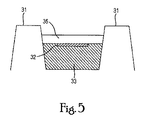
[0050] 図5は、本発明の一実施形態に係る静電クランプの最上層の一部断面を示している。図4に示す実施形態において、電極32は絶縁体33、35に囲まれ、バール31間に設けられる。一実施形態において、絶縁体は誘電体材料から形成され得る。図5の実施形態において、誘電体材料35は電極32の上方に設けられ、絶縁材料層(誘電体を有し得る)33は電極32の下方に設けられる。誘電体材料としては、例えば、Para Tech Coating,Inc.によるPARYLENE(登録商標)ポリ(p−キシレン)ポリマー、E.I. du Pont de Nemours and CompanyによるKAPTON(登録商標)ポリイミドもしくはMYLAR(登録商標)ポリエステル、または液晶ポリマー(LCP)などのプラスチックが挙げられる。SCHOTT(登録商標)封着ガラス、SCHOTT(登録商標)AF37またはSCHOTT BOROFLOAT(登録商標)33などの石英が誘電体材料として用いられ得る。絶縁体および/または誘電体として用いられ得る別の材料は、窒化ホウ素であり得る。
FIG. 5 shows a partial cross section of the uppermost layer of the electrostatic clamp according to one embodiment of the present invention. In the embodiment shown in FIG. 4, the electrode 32 is surrounded by
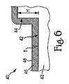
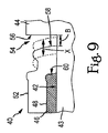
[0051] 図6〜図9は、本発明の一実施形態に係る静電クランプに2つ以上の層を塗布する製造方法の工程の詳細な部分断面図である。すなわち、本明細書記載の実施形態において、誘電体材料(例えば、PARYLENE(登録商標))の2つ以上の層が静電クランプのサポート上に塗布され、アルミニウム電極がバール間に位置し、誘電体層によって囲まれる。本実施形態の複数の誘電体層は、放射(例えば、EUV放射)を照射する際、最小限の固有の絶縁破壊強度を増加させ、誘電体層の局所破壊を低減させる。誘電体層の数の増加によって電極の周囲の厚さを増加させることができ、従って、クランプ領域あたりの不良の数の低下をもたらすことができる。例えば、多くの誘電体不良は欠陥によるものである。複数の層を用いることによってどの層において欠陥の影響を軽減することができ、より最小の絶縁破壊強度がもたらされる。また、クランプを歪めるまたは変形させるパワーまたは力は、層の厚さに正比例する。つまり、誘電体層の厚さが増加するにつれて、強度も増加し、それによってクランプの変形しやすさが低下する。 FIGS. 6 to 9 are detailed partial cross-sectional views of the steps of the manufacturing method for applying two or more layers to the electrostatic clamp according to the embodiment of the present invention. That is, in the embodiments described herein, two or more layers of dielectric material (eg, PARYLENE®) are applied on the support of the electrostatic clamp, the aluminum electrode is positioned between the bars, and the dielectric Surrounded by body layers. The plurality of dielectric layers of this embodiment increase the minimum intrinsic breakdown strength and reduce local breakdown of the dielectric layer when irradiated with radiation (eg, EUV radiation). Increasing the number of dielectric layers can increase the perimeter thickness of the electrode, thus reducing the number of defects per clamp area. For example, many dielectric defects are due to defects. By using multiple layers, the effect of defects in any layer can be reduced, resulting in a minimum dielectric breakdown strength. Also, the power or force that distorts or deforms the clamp is directly proportional to the layer thickness. That is, as the thickness of the dielectric layer increases, the strength also increases, thereby reducing the ease of deformation of the clamp.
[0052] 図6〜図9は、物体を(図4に示す方法と同様の方法で)実質的な固定平面に保持するように構成された静電クランプ40を製造する工程の詳細な図である。静電クランプ40は、基部43と、基部43から延在する複数のバール44とを含むサポートまたはテーブル42を含む。複数のバール44の各々は、頂部および底部を含む。バール44は、底部(またはサポート42の表面)から頂部まで測定される高さHを有する。一実施形態において、バール44は、約85μmの範囲の高さHで設けられる。一実施形態において、バールの頂部は物体が保持される平面を決定する。
[0052] FIGS. 6-9 are detailed views of a process for manufacturing an
[0053] 図6は、サポート42およびそのバール44に対する材料の第1層46が設けられるまたは塗布される、サポート42の表面を示している。第1層46は、基部43とバール44の頂部に対して設けられる。また、電極層48が、少なくともバール44間に設けられる、または塗布される。図示の実施形態において、電極48は、第1層46、基部43、およびバール44の頂部の上に完全に塗布される。
[0053] FIG. 6 shows the surface of the
[0054] 一実施形態において、第1層46は誘電体材料を含む。一実施形態において、第1層46はプラスチックを含む。一実施形態において、第1層46はPARYLENE(登録商標)を含む。
[0054] In one embodiment, the
[0055] 一実施形態において、電極48はアルミニウムを含む。
[0055] In one embodiment, the
[0056] サポート42の表面上に設けられる、または塗布される第1層46の厚さTは、限定されるべきでない。一実施形態において、材料の第1層46の厚さTは、約20ミクロン以上かつ約30ミクロン以下である。一実施形態において、第1層46の厚さTは約25ミクロンである。一実施形態において、電極の厚さは約300nmである。
[0056] The thickness T of the
[0057] 次のステップにおいて、図7に示すように、サポート42の表面から、少なくとも第1層46をエッチングする。すなわち、複数のバール44に対して、および/または複数のバール44の周囲に、第1凹み50が少なくとも第1層46において形成されるように、少なくとも第1層46をエッチングし、それにより、第1層46は、バール44のエッジ56から第1距離Aだけ離れる。また、バール44から、電極層48をエッチングし得る。一実施形態において、第1凹み50は、各バール44のエッジ56から約100ミクロンだけ第1層46および電極層48をエッチングすることによって形成される(すなわち、A=約100ミクロン)。一実施形態において、第1層46をエッチングする量は、距離A+/−Xミクロンである。一実施形態において、バール44から約100+/−25ミクロンだけ第1層46をエッチングする。
In the next step, as shown in FIG. 7, at least the
[0058] 図8において、サポート42に、基部43に対する(第1層46、第1凹み50、および複数のバール44の頂部の上に、を含む)材料の第2層52が設けられる、または塗布される。一実施形態において、第2層52は誘電体材料を含む。一実施形態において、第2層52はプラスチックを含む。一実施形態において、第2層52はPARYLENE(登録商標)を含む。
[0058] In FIG. 8, the
[0059] 一実施形態において、第1層46および第2層52は同様の材料を含む。一実施形態において、第1層46および第2層52はともにPARYLENE(登録商標)を含む。
[0059] In one embodiment, the
[0060] サポート42の表面上(第1層46、第1凹み50、およびバール44に対する、を含む)に設けられる、または塗布される第2層52の厚さT2は、限定されるべきでない。一実施形態において、第2層52の厚さT2は、約40ミクロン以上かつ約60ミクロン以下である。一実施形態において、第2層52の厚さT2は約50ミクロンである。一実施形態において、第2層52がサポート42の表面上に塗布される際、第2層52の厚さT2は実質的に均一である。一実施形態において、第2層52の厚さT2は、サポート42の表面に沿って均一でなくてよい。
[0060] The thickness T2 of the
[0061] そして、図9に示すように、サポート42の表面から、少なくとも第2層52をエッチングする。すなわち、複数のバール44に対して、および/または複数のバール44の周囲に、第2凹み54が少なくとも第2層52において形成されるように、少なくとも第2層52をエッチングし、それにより、第2層52は、バール44のエッジ56から第2距離Bだけ離れる。一実施形態において、第2凹み54は、各バール44から約25ミクロンだけ第2層52をエッチングすることによって形成される(すなわち、B=約25ミクロン)。一実施形態において、第2層52をエッチングする量は、距離B+/−Xミクロンである(ここで、Xは第1層46についての値と同じ値である必要はない)。一実施形態において、バール44のエッジ56から約25+/−25ミクロンだけ第2層52をエッチングする。一実施形態において、距離Bは距離Aより短い。
Then, as shown in FIG. 9, at least the
[0062] 第1および第2層46、52の塗布は限定されるべきでない。例えば、一実施形態において、第1層46および/または第2層52は、スパッタリングプロセスを用いて、化学蒸着プロセス、またはその組合せを用いてサポート上に設けられる。さらに、第1および第2層46、52のエッチング(すなわち、第1および第2凹み50、54のエッチング)は、あらゆる方法で行われて良く、限定されるべきでない。一実施形態において、第1および第2凹みを形成するために、レーザアブレーションプロセスが利用される。
[0062] The application of the first and
[0063] 図10は、本発明の一実施形態に係る、図6〜図9に示すエッチングおよび処理の後の、サポート42上のバール44の、上方からの詳細な上面図である。バール44は、バール44のエッジ56と第2層52のエッジ58との間に実質的に形成された第2凹み54を有する。第1層46および電極48のエッジ60は、図10において破線によっておおむね表されている(というのは、それらの層は、図7に示すように、バール44から、層46および48を第1距離Aだけエッチングすることにより、第2層52の下に設けられるからである)。
[0063] FIG. 10 is a detailed top view from above of the
[0064] 一実施形態において、第1層46および第2層52は誘電体材料を含む。一実施形態において、第1層46および第2層52はPARYLENE(登録商標)を含む。
[0064] In one embodiment, the
[0065] 一実施形態において、バール44は、約500ミクロンの直径を有する。材料の第1層46および電極層48は、バール44の周囲から、最大約700+/−ミクロンの直径だけ除去され得る。材料の第2層52は、バール44を囲む最大約550+/−ミクロンの直径だけ除去され得る。
[0065] In one embodiment, the
[0066] 1つのバール44の一部しか図6〜図10に示されていないが、通常、複数のバールが用いられ得ることと、電極48および材料層46、52がそれらのバール44の各々の間に位置し得ることとが明らかである。図11は、本発明の一実施形態に係る、基部と複数のバール44とを有するサポート42の詳細な平面図である。一実施形態において、バール44を備えたサポート42は1つの材料から形成されてよく、それにより、サポート42上のバール44の位置が安定し固定され、これは、物体を平面内の当該位置上で安定して保持するのに役立つ。
[0066] Although only a portion of one
[0067] 安定性を向上させるために、サポート42は、バール44の高さの10〜200倍とすることができる。例えば、一実施形態において、約85μmのバールの高さHで、サポートは直径約500μmを有し得る。隣接するバールの中心62間の距離Cは、最大約2mm(ミリメートル)であり得る。
[0067] In order to improve stability, the
[0068] バールの中心62から層52、48、および46のエッジ58までの距離Dは、限定されるべきでない。バールの中心62を用いて、例えば2mm×2mmすなわち4mm2の領域を形成することによって、正方形単位セル(square unit cell)が測定され得る。一実施形態において、バールの中心62から層52、48、および46のエッジ58までの距離Dは、約375μmであり得る。4mm2によって形成された領域は、層46、52および電極48の約89%を覆い得る。
[0068] The distance D from the
[0069] 一実施形態において、電極48とバール44の頂部との間の距離は、50〜1000μmであり得る。
[0069] In one embodiment, the distance between the
[0070] 図6〜図9の実施形態のサポート42、その基部43、および複数のバール44ならびに図10および図11に示す実施形態は、1つ以上の材料から形成されてよく(当該材料は上記に開示した材料を含むが、これらに限定されない)、限定的であるべきでない。
[0070] The
[0071] 本明細書において、IC製造におけるリソグラフィ装置の使用について具体的な言及がなされているが、本明細書記載のリソグラフィ装置が、集積光学システム、磁気ドメインメモリ用のガイダンスパターンおよび検出パターン、フラットパネルディスプレイ、液晶ディスプレイ(LCD)、薄膜磁気ヘッド等の製造といった他の用途を有し得ることが理解されるべきである。当業者にとっては当然のことであるが、そのような別の用途においては、本明細書で使用される「ウェーハ」または「ダイ」という用語はすべて、それぞれより一般的な「基板」または「ターゲット部分」という用語と同義であるとみなしてよい。本明細書に記載した基板は、露光の前後を問わず、例えば、トラック(通常、基板にレジスト層を塗布し、かつ露光されたレジストを現像するツール)、メトロロジーツール、および/またはインスペクションツールで処理されてもよい。適用可能な場合には、本明細書中の開示内容を上記のような基板プロセシングツールおよびその他の基板プロセシングツールに適用してもよい。さらに基板は、例えば、多層ICを作るために複数回処理されてもよいので、本明細書で使用される基板という用語は、すでに多重処理層を包含している基板を表すものとしてもよい。 [0071] Although specific reference is made herein to the use of a lithographic apparatus in IC manufacturing, the lithographic apparatus described herein is an integrated optical system, a guidance pattern and a detection pattern for a magnetic domain memory, It should be understood that other applications such as the manufacture of flat panel displays, liquid crystal displays (LCDs), thin film magnetic heads and the like may be had. As will be appreciated by those skilled in the art, in such other applications, the terms “wafer” or “die” as used herein are all more general “substrate” or “target” respectively. It may be considered synonymous with the term “part”. The substrate described herein can be used, for example, before or after exposure, such as a track (usually a tool for applying a resist layer to the substrate and developing the exposed resist), a metrology tool, and / or an inspection tool. May be processed. Where applicable, the disclosure herein may be applied to substrate processing tools such as those described above and other substrate processing tools. Further, since the substrate may be processed multiple times, for example, to make a multi-layer IC, the term substrate as used herein may refer to a substrate that already contains multiple processing layers.
[0072] 光リソグラフィの関連での本発明の実施形態の使用について上述のとおり具体的な言及がなされたが、当然のことながら、本発明は、他の用途、例えば、インプリントリソグラフィに使われてもよく、さらに状況が許すのであれば、光リソグラフィに限定されることはない。インプリントリソグラフィにおいては、パターニングデバイス内のトポグラフィによって、基板上に創出されるパターンが定義される。パターニングデバイスのトポグラフィは、基板に供給されたレジスト層の中にプレス加工され、基板上では、電磁放射、熱、圧力、またはそれらの組合せによってレジストは硬化される。パターニングデバイスは、レジストが硬化した後、レジスト内にパターンを残してレジストの外へ移動される。 [0072] Although specific reference has been made to the use of embodiments of the present invention in the context of optical lithography as described above, it will be appreciated that the present invention may be used in other applications, such as imprint lithography. However, it is not limited to optical lithography if the situation permits. In imprint lithography, the topography within the patterning device defines the pattern that is created on the substrate. The topography of the patterning device is pressed into a resist layer supplied to the substrate, whereupon the resist is cured by electromagnetic radiation, heat, pressure, or a combination thereof. The patterning device is moved out of the resist leaving a pattern in it after the resist is cured.
[0073] 本明細書で使用される「放射」および「ビーム」という用語は、紫外線(UV)(例えば、365nm、355nm、248nm、193nm、157nm、または126nmの波長、またはおよそこれらの値の波長を有する)、および極端紫外線(EUV)(例えば、5〜20nmの範囲の波長を有する)、ならびにイオンビームや電子ビームなどの微粒子ビームを含むあらゆる種類の電磁放射を包含している。 [0073] As used herein, the terms "radiation" and "beam" refer to ultraviolet (UV) (eg, wavelengths of 365 nm, 355 nm, 248 nm, 193 nm, 157 nm, or 126 nm, or about these wavelengths) ), And extreme ultraviolet (EUV) (e.g., having a wavelength in the range of 5-20 nm), and all types of electromagnetic radiation, including particulate beams such as ion beams and electron beams.
[0074] 「レンズ」という用語は、文脈によっては、屈折、反射、磁気、電磁気、および静電型光学コンポーネントを含む様々な種類の光学コンポーネントのいずれか1つまたはこれらの組合せを指すことができる。 [0074] The term "lens" can refer to any one or combination of various types of optical components, including refractive, reflective, magnetic, electromagnetic, and electrostatic optical components, depending on the context. .
[0075] 上記の説明は、制限ではなく例示を意図したものである。従って、当業者には明らかなように、添付の特許請求の範囲を逸脱することなく本記載の発明に変更を加えてもよい。 [0075] The descriptions above are intended to be illustrative, not limiting. Thus, it will be apparent to one skilled in the art that modifications may be made to the invention as described without departing from the scope of the claims set out below.
Claims (13)
基部と該基部から延在する複数のバールとを含むサポートであって、該複数のバールの各々は頂部と底部とを含み、該バールの該頂部は前記物体が保持される平面を決定する、サポートと、
隣接するバール間に設けられた材料の第1層および材料の第2層であって、該第1層および該第2層は該隣接するバールの頂部より高く延在せず、該隣接するバールの底部より低く延在しない、第1層および第2層と、
前記隣接するバール間に設けられ、かつ前記第1層および前記第2層によって囲まれた電極と、を備え、
前記第1層は、各バールから第1距離だけ離れて設けられ、
前記第2層は、前記第1層と前記バールとの間の前記第1距離によって形成された領域の少なくとも一部内に設けられる、
静電クランプ。 An electrostatic clamp for holding an object on a substantially fixed surface,
A support including a base and a plurality of bars extending from the base, each of the plurality of bars including a top and a bottom, the top of the bar determining a plane in which the object is held; Support,
A first layer of material and a second layer of material provided between adjacent bars, wherein the first layer and the second layer do not extend higher than the top of the adjacent bar, and the adjacent bar A first layer and a second layer that do not extend below the bottom of the
An electrode provided between the adjacent bars and surrounded by the first layer and the second layer;
The first layer is provided at a first distance from each bar;
The second layer is provided in at least a portion of a region formed by the first distance between the first layer and the burl;
Electrostatic clamp.
前記基部および前記バールの頂部の上に材料の第1層を設けることと、
前記第1層を含んで、前記基部および前記バールの上に電極を設けることと、
少なくとも前記第1層が前記バールから前記第1距離だけ離れるように、少なくとも第1層において前記複数のバールの周囲に第1凹みをエッチングで形成することと、
前記第1層を含む前記基部、前記第1凹み、および前記バールの前記頂部の上に材料の第2層を設けることと、
少なくとも前記材料の第2層が前記バールから前記第2距離だけ離れるように、少なくとも第2層において前記複数のバールの周囲に第2凹みをエッチングで形成することと、を含む、方法。 A method of manufacturing an electrostatic clamp for electrostatically clamping an object to an object support, the electrostatic clamp comprising a base and a plurality of bars extending from the base, the method comprising: Each of the plurality of bars includes a top and a bottom, the top of the bar comprising a support that determines a plane in which the object is held, the method comprising:
Providing a first layer of material on the base and the top of the burl;
Including the first layer and providing electrodes on the base and the burl;
Etching at least the first layer around the plurality of bars so that at least the first layer is separated from the burl by the first distance; and
Providing a second layer of material on the base including the first layer, the first recess, and the top of the burl;
Etching a second recess at least around the plurality of bars in the second layer such that at least a second layer of the material is separated from the burl by the second distance.
放射ビームのビーム経路において物体を支持する物体サポートと、
前記物体サポートに対して前記物体を静電的にクランプする静電クランプであって、
基部と該基部から延在する複数のバールとを含むサポートであって、該複数のバールの各々は頂部と底部とを含み、該バールの該頂部は前記物体が保持される平面を決定する、サポートと、
隣接するバール間に設けられた材料の第1層および材料の第2層であって、該第1層および該第2層は該隣接するバールの頂部より高く延在せず、該隣接するバールの底部より低く延在しない、第1層および第2層と、
前記隣接するバール間に設けられ、かつ前記第1層および前記第2層によって囲まれた電極と、を備える、静電クランプと、を備え、
前記第1層は、各バールから第1距離だけ離れて設けられ、
前記第2層は、前記第1層と前記バールとの間の前記第1距離によって形成された領域の少なくとも一部内に設けられる、
装置。 A device,
An object support that supports the object in the beam path of the radiation beam;
An electrostatic clamp that electrostatically clamps the object against the object support,
A support including a base and a plurality of bars extending from the base, each of the plurality of bars including a top and a bottom, the top of the bar determining a plane in which the object is held; Support,
A first layer of material and a second layer of material provided between adjacent bars, wherein the first layer and the second layer do not extend higher than the top of the adjacent bar, and the adjacent bar A first layer and a second layer that do not extend below the bottom of the
An electrostatic clamp comprising: an electrode provided between the adjacent bars and surrounded by the first layer and the second layer;
The first layer is provided at a first distance from each bar;
The second layer is provided in at least a portion of a region formed by the first distance between the first layer and the burl;
apparatus.
The apparatus is a lithographic apparatus, wherein the patterning device support holds a patterning device that patterns the radiation beam to form a patterned radiation beam, a substrate support that holds the substrate, and a patterned radiation beam projected onto the substrate The apparatus according to any one of claims 10 to 12, wherein the object support is the patterning device or the substrate support.
Applications Claiming Priority (3)
| Application Number | Priority Date | Filing Date | Title |
|---|---|---|---|
| US42107610P | 2010-12-08 | 2010-12-08 | |
| US61/421,076 | 2010-12-08 | ||
| PCT/EP2011/066387 WO2012076207A1 (en) | 2010-12-08 | 2011-09-21 | Electrostatic clamp, lithographic apparatus and method of manufacturing an electrostatic clamp |
Publications (3)
| Publication Number | Publication Date |
|---|---|
| JP2014502053A JP2014502053A (en) | 2014-01-23 |
| JP2014502053A5 JP2014502053A5 (en) | 2014-11-06 |
| JP5960154B2 true JP5960154B2 (en) | 2016-08-02 |
Family
ID=44653342
Family Applications (1)
| Application Number | Title | Priority Date | Filing Date |
|---|---|---|---|
| JP2013542421A Active JP5960154B2 (en) | 2010-12-08 | 2011-09-21 | Electrostatic clamp, lithographic apparatus, and method of manufacturing electrostatic clamp |
Country Status (5)
| Country | Link |
|---|---|
| US (1) | US9348236B2 (en) |
| JP (1) | JP5960154B2 (en) |
| NL (1) | NL2007452A (en) |
| TW (1) | TWI527150B (en) |
| WO (1) | WO2012076207A1 (en) |
Families Citing this family (13)
| Publication number | Priority date | Publication date | Assignee | Title |
|---|---|---|---|---|
| WO2014012749A1 (en) | 2012-07-17 | 2014-01-23 | Asml Netherlands B.V. | Electrostatic clamp, lithographic apparatus and method |
| DE102014008029B4 (en) | 2014-05-28 | 2023-05-17 | Asml Netherlands B.V. | Electrostatic chuck having an electrode support disc and method of making the chuck |
| DE102014008031B4 (en) | 2014-05-28 | 2020-06-25 | Berliner Glas Kgaa Herbert Kubatz Gmbh & Co. | Electrostatic holding device with a ceramic electrode and method for producing such a holding device |
| DE102014008030A1 (en) | 2014-05-28 | 2015-12-03 | Berliner Glas Kgaa Herbert Kubatz Gmbh & Co | Method of making an electrostatic chuck |
| DE102014007903A1 (en) | 2014-05-28 | 2015-12-03 | Berliner Glas Kgaa Herbert Kubatz Gmbh & Co. | Electrostatic holding device with nubbed electrodes and method for their production |
| KR102590964B1 (en) * | 2016-07-20 | 2023-10-18 | 삼성디스플레이 주식회사 | Electro-static chuck |
| DE102018116463A1 (en) | 2018-07-06 | 2020-01-09 | Berliner Glas Kgaa Herbert Kubatz Gmbh & Co. | Electrostatic chuck and method of making the same |
| NL2025069A (en) * | 2019-03-13 | 2020-09-17 | Asml Holding Nv | Electrostatic clamp for a lithographic apparatus |
| DE102019108855B4 (en) * | 2019-04-04 | 2020-11-12 | Berliner Glas Kgaa Herbert Kubatz Gmbh & Co. | Electrostatic holding device with a layer composite electrode device and method for its production |
| KR20220010725A (en) * | 2019-05-29 | 2022-01-26 | 에이에스엠엘 홀딩 엔.브이. | Split double-sided wafer and reticle clamp |
| DE102020104238A1 (en) | 2020-02-18 | 2021-08-19 | Berliner Glas GmbH | Method and polishing device for processing a plate-shaped component, and plate-shaped component, in particular electrostatic holding device or immersion wafer board |
| KR20230149310A (en) | 2021-03-02 | 2023-10-26 | 에이에스엠엘 네델란즈 비.브이. | Operation of metrology systems, lithographic apparatus, and methods thereof |
| DE102021115970A1 (en) | 2021-06-21 | 2022-12-22 | Asml Netherlands B.V. | Holding device for holding components and method for producing the holding device |
Family Cites Families (32)
| Publication number | Priority date | Publication date | Assignee | Title |
|---|---|---|---|---|
| GB2106325A (en) * | 1981-09-14 | 1983-04-07 | Philips Electronic Associated | Electrostatic chuck |
| JPH07142555A (en) | 1993-06-29 | 1995-06-02 | Hitachi Ltd | Wafer chuck |
| EP0669644B1 (en) * | 1994-02-28 | 1997-08-20 | Applied Materials, Inc. | Electrostatic chuck |
| JP3954177B2 (en) * | 1997-01-29 | 2007-08-08 | 日本碍子株式会社 | Bonding structure between metal member and ceramic member and method for manufacturing the same |
| US6117246A (en) | 1997-01-31 | 2000-09-12 | Applied Materials, Inc. | Conductive polymer pad for supporting a workpiece upon a workpiece support surface of an electrostatic chuck |
| US5880924A (en) | 1997-12-01 | 1999-03-09 | Applied Materials, Inc. | Electrostatic chuck capable of rapidly dechucking a substrate |
| US6107192A (en) * | 1997-12-30 | 2000-08-22 | Applied Materials, Inc. | Reactive preclean prior to metallization for sub-quarter micron application |
| JP2000340640A (en) | 1999-05-31 | 2000-12-08 | Toto Ltd | Non-contacting electrostatically attracting apparatus |
| JP2001244177A (en) | 2000-02-28 | 2001-09-07 | Nikon Corp | Stage apparatus and holder, scanning aligner and aligner |
| DE10157487C1 (en) | 2001-11-23 | 2003-06-18 | Sgl Carbon Ag | Fiber-reinforced composite body for protective armor, its manufacture and uses |
| US6673714B2 (en) * | 2002-04-25 | 2004-01-06 | Hewlett-Packard Development Company, L.P. | Method of fabricating a sub-lithographic sized via |
| KR100511854B1 (en) | 2002-06-18 | 2005-09-02 | 아네르바 가부시키가이샤 | Electrostatic chuck device |
| JP4010541B2 (en) * | 2002-06-18 | 2007-11-21 | キヤノンアネルバ株式会社 | Electrostatic adsorption device |
| US20030233977A1 (en) | 2002-06-20 | 2003-12-25 | Yeshwanth Narendar | Method for forming semiconductor processing components |
| US7092231B2 (en) | 2002-08-23 | 2006-08-15 | Asml Netherlands B.V. | Chuck, lithographic apparatus and device manufacturing method |
| US6835415B2 (en) | 2003-01-07 | 2004-12-28 | Euv Llc | Compliant layer chucking surface |
| JP4472372B2 (en) | 2003-02-03 | 2010-06-02 | 株式会社オクテック | Plasma processing apparatus and electrode plate for plasma processing apparatus |
| US6897945B1 (en) * | 2003-12-15 | 2005-05-24 | Asml Netherlands B.V. | Lithographic apparatus and device manufacturing method |
| US7133120B2 (en) | 2004-05-04 | 2006-11-07 | Asml Netherlands B.V. | Lithographic apparatus, article support member, and method |
| US20070097346A1 (en) | 2005-10-28 | 2007-05-03 | Asml Netherlands B.V. | Lithographic apparatus and device manufacturing method |
| US7564536B2 (en) | 2005-11-08 | 2009-07-21 | Asml Netherlands B.V. | Lithographic apparatus and device manufacturing method |
| US7646581B2 (en) | 2006-01-31 | 2010-01-12 | Sumitomo Osaka Cement Co., Ltd. | Electrostatic chuck |
| US8325321B2 (en) | 2006-07-28 | 2012-12-04 | Mapper Lithography Ip B.V. | Lithography system, method of heat dissipation and frame |
| US7715170B2 (en) * | 2007-03-26 | 2010-05-11 | Varian Semiconductor Equipment Associates, Inc. | Electrostatic chuck with separated electrodes |
| US7940511B2 (en) * | 2007-09-21 | 2011-05-10 | Asml Netherlands B.V. | Electrostatic clamp, lithographic apparatus and method of manufacturing an electrostatic clamp |
| JP4974873B2 (en) | 2007-12-26 | 2012-07-11 | 新光電気工業株式会社 | Electrostatic chuck and substrate temperature control fixing device |
| TWI475594B (en) * | 2008-05-19 | 2015-03-01 | Entegris Inc | Electrostatic chuck |
| KR100984177B1 (en) * | 2008-06-13 | 2010-09-28 | 엘아이지에이디피 주식회사 | Electrostatic chuck and plasma ion implantation apparatus using the same |
| US20100063568A1 (en) * | 2008-09-11 | 2010-03-11 | Staunton Douglas A | Implantable electrode array assembly with extraction sleeve/tether |
| JP2010161319A (en) * | 2009-01-09 | 2010-07-22 | Nikon Corp | Electrostatic chucking device, exposure apparatus, and device manufacturing method |
| JP5453902B2 (en) * | 2009-04-27 | 2014-03-26 | Toto株式会社 | Electrostatic chuck and method of manufacturing electrostatic chuck |
| JP2011192991A (en) * | 2010-03-12 | 2011-09-29 | Asml Netherlands Bv | Lithographic apparatus and method |
-
2011
- 2011-09-21 US US13/991,089 patent/US9348236B2/en active Active
- 2011-09-21 WO PCT/EP2011/066387 patent/WO2012076207A1/en active Application Filing
- 2011-09-21 JP JP2013542421A patent/JP5960154B2/en active Active
- 2011-09-21 NL NL2007452A patent/NL2007452A/en not_active Application Discontinuation
- 2011-10-06 TW TW100136322A patent/TWI527150B/en active
Also Published As
| Publication number | Publication date |
|---|---|
| JP2014502053A (en) | 2014-01-23 |
| US20130308116A1 (en) | 2013-11-21 |
| NL2007452A (en) | 2012-06-11 |
| TW201232696A (en) | 2012-08-01 |
| US9348236B2 (en) | 2016-05-24 |
| WO2012076207A1 (en) | 2012-06-14 |
| TWI527150B (en) | 2016-03-21 |
Similar Documents
| Publication | Publication Date | Title |
|---|---|---|
| JP5960154B2 (en) | Electrostatic clamp, lithographic apparatus, and method of manufacturing electrostatic clamp | |
| JP5524845B2 (en) | Electrostatic clamp, lithographic apparatus and method of manufacturing electrostatic clamp | |
| KR100883610B1 (en) | Lithographic apparatus and method of manufacturing an electrostatic clamp for a lithographic apparatus | |
| JP6145564B2 (en) | Object holder for use in a lithographic apparatus and method for manufacturing an object holder | |
| JP6300432B2 (en) | Electrostatic clamp, lithographic apparatus and method of manufacturing electrostatic clamp | |
| JP5210354B2 (en) | Coil, positioning device, actuator, and lithographic projection apparatus | |
| JP4599334B2 (en) | Method for manufacturing article support member | |
| US7245357B2 (en) | Lithographic apparatus and device manufacturing method | |
| KR20070003694A (en) | Lithographic apparatus and device manufacturing method | |
| KR20060135508A (en) | Lithographic apparatus and device manufacturing method | |
| TWI569362B (en) | Electrostatic clamp | |
| CN103415812B (en) | Electrostatic chuck, lithographic equipment and device making method |
Legal Events
| Date | Code | Title | Description |
|---|---|---|---|
| A521 | Request for written amendment filed |
Free format text: JAPANESE INTERMEDIATE CODE: A523 Effective date: 20140919 |
|
| A621 | Written request for application examination |
Free format text: JAPANESE INTERMEDIATE CODE: A621 Effective date: 20140919 |
|
| A977 | Report on retrieval |
Free format text: JAPANESE INTERMEDIATE CODE: A971007 Effective date: 20150826 |
|
| A131 | Notification of reasons for refusal |
Free format text: JAPANESE INTERMEDIATE CODE: A131 Effective date: 20150902 |
|
| A521 | Request for written amendment filed |
Free format text: JAPANESE INTERMEDIATE CODE: A523 Effective date: 20151127 |
|
| A131 | Notification of reasons for refusal |
Free format text: JAPANESE INTERMEDIATE CODE: A131 Effective date: 20160418 |
|
| A521 | Request for written amendment filed |
Free format text: JAPANESE INTERMEDIATE CODE: A523 Effective date: 20160428 |
|
| TRDD | Decision of grant or rejection written | ||
| A01 | Written decision to grant a patent or to grant a registration (utility model) |
Free format text: JAPANESE INTERMEDIATE CODE: A01 Effective date: 20160526 |
|
| A61 | First payment of annual fees (during grant procedure) |
Free format text: JAPANESE INTERMEDIATE CODE: A61 Effective date: 20160622 |
|
| R150 | Certificate of patent or registration of utility model |
Ref document number: 5960154 Country of ref document: JP Free format text: JAPANESE INTERMEDIATE CODE: R150 |
|
| R250 | Receipt of annual fees |
Free format text: JAPANESE INTERMEDIATE CODE: R250 |
|
| R250 | Receipt of annual fees |
Free format text: JAPANESE INTERMEDIATE CODE: R250 |
|
| R250 | Receipt of annual fees |
Free format text: JAPANESE INTERMEDIATE CODE: R250 |
|
| R250 | Receipt of annual fees |
Free format text: JAPANESE INTERMEDIATE CODE: R250 |
|
| R250 | Receipt of annual fees |
Free format text: JAPANESE INTERMEDIATE CODE: R250 |