JP5716637B2 - 半導体モジュール及び半導体モジュールの製造方法 - Google Patents
半導体モジュール及び半導体モジュールの製造方法 Download PDFInfo
- Publication number
- JP5716637B2 JP5716637B2 JP2011241856A JP2011241856A JP5716637B2 JP 5716637 B2 JP5716637 B2 JP 5716637B2 JP 2011241856 A JP2011241856 A JP 2011241856A JP 2011241856 A JP2011241856 A JP 2011241856A JP 5716637 B2 JP5716637 B2 JP 5716637B2
- Authority
- JP
- Japan
- Prior art keywords
- semiconductor module
- base
- circuit board
- semiconductor
- groove
- Prior art date
- Legal status (The legal status is an assumption and is not a legal conclusion. Google has not performed a legal analysis and makes no representation as to the accuracy of the status listed.)
- Expired - Fee Related
Links
Images


Classifications
-
- H—ELECTRICITY
- H01—ELECTRIC ELEMENTS
- H01L—SEMICONDUCTOR DEVICES NOT COVERED BY CLASS H10
- H01L21/00—Processes or apparatus adapted for the manufacture or treatment of semiconductor or solid state devices or of parts thereof
- H01L21/02—Manufacture or treatment of semiconductor devices or of parts thereof
- H01L21/04—Manufacture or treatment of semiconductor devices or of parts thereof the devices having potential barriers, e.g. a PN junction, depletion layer or carrier concentration layer
- H01L21/50—Assembly of semiconductor devices using processes or apparatus not provided for in a single one of the groups H01L21/18 - H01L21/326 or H10D48/04 - H10D48/07 e.g. sealing of a cap to a base of a container
-
- H—ELECTRICITY
- H01—ELECTRIC ELEMENTS
- H01L—SEMICONDUCTOR DEVICES NOT COVERED BY CLASS H10
- H01L23/00—Details of semiconductor or other solid state devices
- H01L23/02—Containers; Seals
- H01L23/04—Containers; Seals characterised by the shape of the container or parts, e.g. caps, walls
- H01L23/043—Containers; Seals characterised by the shape of the container or parts, e.g. caps, walls the container being a hollow construction and having a conductive base as a mounting as well as a lead for the semiconductor body
- H01L23/049—Containers; Seals characterised by the shape of the container or parts, e.g. caps, walls the container being a hollow construction and having a conductive base as a mounting as well as a lead for the semiconductor body the other leads being perpendicular to the base
-
- H—ELECTRICITY
- H01—ELECTRIC ELEMENTS
- H01L—SEMICONDUCTOR DEVICES NOT COVERED BY CLASS H10
- H01L25/00—Assemblies consisting of a plurality of semiconductor or other solid state devices
- H01L25/03—Assemblies consisting of a plurality of semiconductor or other solid state devices all the devices being of a type provided for in a single subclass of subclasses H10B, H10D, H10F, H10H, H10K or H10N, e.g. assemblies of rectifier diodes
- H01L25/04—Assemblies consisting of a plurality of semiconductor or other solid state devices all the devices being of a type provided for in a single subclass of subclasses H10B, H10D, H10F, H10H, H10K or H10N, e.g. assemblies of rectifier diodes the devices not having separate containers
- H01L25/07—Assemblies consisting of a plurality of semiconductor or other solid state devices all the devices being of a type provided for in a single subclass of subclasses H10B, H10D, H10F, H10H, H10K or H10N, e.g. assemblies of rectifier diodes the devices not having separate containers the devices being of a type provided for in group subclass H10D
- H01L25/072—Assemblies consisting of a plurality of semiconductor or other solid state devices all the devices being of a type provided for in a single subclass of subclasses H10B, H10D, H10F, H10H, H10K or H10N, e.g. assemblies of rectifier diodes the devices not having separate containers the devices being of a type provided for in group subclass H10D the devices being arranged next to each other
-
- H—ELECTRICITY
- H01—ELECTRIC ELEMENTS
- H01L—SEMICONDUCTOR DEVICES NOT COVERED BY CLASS H10
- H01L25/00—Assemblies consisting of a plurality of semiconductor or other solid state devices
- H01L25/18—Assemblies consisting of a plurality of semiconductor or other solid state devices the devices being of the types provided for in two or more different main groups of the same subclass of H10B, H10D, H10F, H10H, H10K or H10N
-
- H—ELECTRICITY
- H01—ELECTRIC ELEMENTS
- H01L—SEMICONDUCTOR DEVICES NOT COVERED BY CLASS H10
- H01L2224/00—Indexing scheme for arrangements for connecting or disconnecting semiconductor or solid-state bodies and methods related thereto as covered by H01L24/00
- H01L2224/01—Means for bonding being attached to, or being formed on, the surface to be connected, e.g. chip-to-package, die-attach, "first-level" interconnects; Manufacturing methods related thereto
- H01L2224/26—Layer connectors, e.g. plate connectors, solder or adhesive layers; Manufacturing methods related thereto
- H01L2224/28—Structure, shape, material or disposition of the layer connectors prior to the connecting process
- H01L2224/29—Structure, shape, material or disposition of the layer connectors prior to the connecting process of an individual layer connector
- H01L2224/29001—Core members of the layer connector
- H01L2224/29099—Material
- H01L2224/291—Material with a principal constituent of the material being a metal or a metalloid, e.g. boron [B], silicon [Si], germanium [Ge], arsenic [As], antimony [Sb], tellurium [Te] and polonium [Po], and alloys thereof
- H01L2224/29101—Material with a principal constituent of the material being a metal or a metalloid, e.g. boron [B], silicon [Si], germanium [Ge], arsenic [As], antimony [Sb], tellurium [Te] and polonium [Po], and alloys thereof the principal constituent melting at a temperature of less than 400°C
-
- H—ELECTRICITY
- H01—ELECTRIC ELEMENTS
- H01L—SEMICONDUCTOR DEVICES NOT COVERED BY CLASS H10
- H01L2224/00—Indexing scheme for arrangements for connecting or disconnecting semiconductor or solid-state bodies and methods related thereto as covered by H01L24/00
- H01L2224/01—Means for bonding being attached to, or being formed on, the surface to be connected, e.g. chip-to-package, die-attach, "first-level" interconnects; Manufacturing methods related thereto
- H01L2224/26—Layer connectors, e.g. plate connectors, solder or adhesive layers; Manufacturing methods related thereto
- H01L2224/31—Structure, shape, material or disposition of the layer connectors after the connecting process
- H01L2224/32—Structure, shape, material or disposition of the layer connectors after the connecting process of an individual layer connector
- H01L2224/321—Disposition
- H01L2224/32151—Disposition the layer connector connecting between a semiconductor or solid-state body and an item not being a semiconductor or solid-state body, e.g. chip-to-substrate, chip-to-passive
- H01L2224/32221—Disposition the layer connector connecting between a semiconductor or solid-state body and an item not being a semiconductor or solid-state body, e.g. chip-to-substrate, chip-to-passive the body and the item being stacked
- H01L2224/32225—Disposition the layer connector connecting between a semiconductor or solid-state body and an item not being a semiconductor or solid-state body, e.g. chip-to-substrate, chip-to-passive the body and the item being stacked the item being non-metallic, e.g. insulating substrate with or without metallisation
-
- H—ELECTRICITY
- H01—ELECTRIC ELEMENTS
- H01L—SEMICONDUCTOR DEVICES NOT COVERED BY CLASS H10
- H01L2224/00—Indexing scheme for arrangements for connecting or disconnecting semiconductor or solid-state bodies and methods related thereto as covered by H01L24/00
- H01L2224/01—Means for bonding being attached to, or being formed on, the surface to be connected, e.g. chip-to-package, die-attach, "first-level" interconnects; Manufacturing methods related thereto
- H01L2224/42—Wire connectors; Manufacturing methods related thereto
- H01L2224/47—Structure, shape, material or disposition of the wire connectors after the connecting process
- H01L2224/48—Structure, shape, material or disposition of the wire connectors after the connecting process of an individual wire connector
- H01L2224/4805—Shape
- H01L2224/4809—Loop shape
- H01L2224/48091—Arched
-
- H—ELECTRICITY
- H01—ELECTRIC ELEMENTS
- H01L—SEMICONDUCTOR DEVICES NOT COVERED BY CLASS H10
- H01L2224/00—Indexing scheme for arrangements for connecting or disconnecting semiconductor or solid-state bodies and methods related thereto as covered by H01L24/00
- H01L2224/01—Means for bonding being attached to, or being formed on, the surface to be connected, e.g. chip-to-package, die-attach, "first-level" interconnects; Manufacturing methods related thereto
- H01L2224/42—Wire connectors; Manufacturing methods related thereto
- H01L2224/47—Structure, shape, material or disposition of the wire connectors after the connecting process
- H01L2224/49—Structure, shape, material or disposition of the wire connectors after the connecting process of a plurality of wire connectors
- H01L2224/491—Disposition
- H01L2224/4911—Disposition the connectors being bonded to at least one common bonding area, e.g. daisy chain
- H01L2224/49113—Disposition the connectors being bonded to at least one common bonding area, e.g. daisy chain the connectors connecting different bonding areas on the semiconductor or solid-state body to a common bonding area outside the body, e.g. converging wires
-
- H—ELECTRICITY
- H01—ELECTRIC ELEMENTS
- H01L—SEMICONDUCTOR DEVICES NOT COVERED BY CLASS H10
- H01L2224/00—Indexing scheme for arrangements for connecting or disconnecting semiconductor or solid-state bodies and methods related thereto as covered by H01L24/00
- H01L2224/73—Means for bonding being of different types provided for in two or more of groups H01L2224/10, H01L2224/18, H01L2224/26, H01L2224/34, H01L2224/42, H01L2224/50, H01L2224/63, H01L2224/71
- H01L2224/732—Location after the connecting process
- H01L2224/73251—Location after the connecting process on different surfaces
- H01L2224/73265—Layer and wire connectors
-
- H—ELECTRICITY
- H01—ELECTRIC ELEMENTS
- H01L—SEMICONDUCTOR DEVICES NOT COVERED BY CLASS H10
- H01L23/00—Details of semiconductor or other solid state devices
- H01L23/34—Arrangements for cooling, heating, ventilating or temperature compensation ; Temperature sensing arrangements
- H01L23/36—Selection of materials, or shaping, to facilitate cooling or heating, e.g. heatsinks
- H01L23/373—Cooling facilitated by selection of materials for the device or materials for thermal expansion adaptation, e.g. carbon
- H01L23/3735—Laminates or multilayers, e.g. direct bond copper ceramic substrates
-
- H—ELECTRICITY
- H01—ELECTRIC ELEMENTS
- H01L—SEMICONDUCTOR DEVICES NOT COVERED BY CLASS H10
- H01L23/00—Details of semiconductor or other solid state devices
- H01L23/34—Arrangements for cooling, heating, ventilating or temperature compensation ; Temperature sensing arrangements
- H01L23/42—Fillings or auxiliary members in containers or encapsulations selected or arranged to facilitate heating or cooling
- H01L23/433—Auxiliary members in containers characterised by their shape, e.g. pistons
- H01L23/4334—Auxiliary members in encapsulations
-
- H—ELECTRICITY
- H01—ELECTRIC ELEMENTS
- H01L—SEMICONDUCTOR DEVICES NOT COVERED BY CLASS H10
- H01L24/00—Arrangements for connecting or disconnecting semiconductor or solid-state bodies; Methods or apparatus related thereto
- H01L24/01—Means for bonding being attached to, or being formed on, the surface to be connected, e.g. chip-to-package, die-attach, "first-level" interconnects; Manufacturing methods related thereto
- H01L24/26—Layer connectors, e.g. plate connectors, solder or adhesive layers; Manufacturing methods related thereto
- H01L24/28—Structure, shape, material or disposition of the layer connectors prior to the connecting process
- H01L24/29—Structure, shape, material or disposition of the layer connectors prior to the connecting process of an individual layer connector
-
- H—ELECTRICITY
- H01—ELECTRIC ELEMENTS
- H01L—SEMICONDUCTOR DEVICES NOT COVERED BY CLASS H10
- H01L24/00—Arrangements for connecting or disconnecting semiconductor or solid-state bodies; Methods or apparatus related thereto
- H01L24/01—Means for bonding being attached to, or being formed on, the surface to be connected, e.g. chip-to-package, die-attach, "first-level" interconnects; Manufacturing methods related thereto
- H01L24/26—Layer connectors, e.g. plate connectors, solder or adhesive layers; Manufacturing methods related thereto
- H01L24/31—Structure, shape, material or disposition of the layer connectors after the connecting process
- H01L24/32—Structure, shape, material or disposition of the layer connectors after the connecting process of an individual layer connector
-
- H—ELECTRICITY
- H01—ELECTRIC ELEMENTS
- H01L—SEMICONDUCTOR DEVICES NOT COVERED BY CLASS H10
- H01L24/00—Arrangements for connecting or disconnecting semiconductor or solid-state bodies; Methods or apparatus related thereto
- H01L24/01—Means for bonding being attached to, or being formed on, the surface to be connected, e.g. chip-to-package, die-attach, "first-level" interconnects; Manufacturing methods related thereto
- H01L24/42—Wire connectors; Manufacturing methods related thereto
- H01L24/47—Structure, shape, material or disposition of the wire connectors after the connecting process
- H01L24/48—Structure, shape, material or disposition of the wire connectors after the connecting process of an individual wire connector
-
- H—ELECTRICITY
- H01—ELECTRIC ELEMENTS
- H01L—SEMICONDUCTOR DEVICES NOT COVERED BY CLASS H10
- H01L24/00—Arrangements for connecting or disconnecting semiconductor or solid-state bodies; Methods or apparatus related thereto
- H01L24/01—Means for bonding being attached to, or being formed on, the surface to be connected, e.g. chip-to-package, die-attach, "first-level" interconnects; Manufacturing methods related thereto
- H01L24/42—Wire connectors; Manufacturing methods related thereto
- H01L24/47—Structure, shape, material or disposition of the wire connectors after the connecting process
- H01L24/49—Structure, shape, material or disposition of the wire connectors after the connecting process of a plurality of wire connectors
-
- H—ELECTRICITY
- H01—ELECTRIC ELEMENTS
- H01L—SEMICONDUCTOR DEVICES NOT COVERED BY CLASS H10
- H01L24/00—Arrangements for connecting or disconnecting semiconductor or solid-state bodies; Methods or apparatus related thereto
- H01L24/71—Means for bonding not being attached to, or not being formed on, the surface to be connected
- H01L24/72—Detachable connecting means consisting of mechanical auxiliary parts connecting the device, e.g. pressure contacts using springs or clips
-
- H—ELECTRICITY
- H01—ELECTRIC ELEMENTS
- H01L—SEMICONDUCTOR DEVICES NOT COVERED BY CLASS H10
- H01L2924/00—Indexing scheme for arrangements or methods for connecting or disconnecting semiconductor or solid-state bodies as covered by H01L24/00
- H01L2924/0001—Technical content checked by a classifier
- H01L2924/00014—Technical content checked by a classifier the subject-matter covered by the group, the symbol of which is combined with the symbol of this group, being disclosed without further technical details
-
- H—ELECTRICITY
- H01—ELECTRIC ELEMENTS
- H01L—SEMICONDUCTOR DEVICES NOT COVERED BY CLASS H10
- H01L2924/00—Indexing scheme for arrangements or methods for connecting or disconnecting semiconductor or solid-state bodies as covered by H01L24/00
- H01L2924/10—Details of semiconductor or other solid state devices to be connected
- H01L2924/102—Material of the semiconductor or solid state bodies
- H01L2924/1025—Semiconducting materials
- H01L2924/1026—Compound semiconductors
- H01L2924/1027—IV
- H01L2924/10272—Silicon Carbide [SiC]
-
- H—ELECTRICITY
- H01—ELECTRIC ELEMENTS
- H01L—SEMICONDUCTOR DEVICES NOT COVERED BY CLASS H10
- H01L2924/00—Indexing scheme for arrangements or methods for connecting or disconnecting semiconductor or solid-state bodies as covered by H01L24/00
- H01L2924/10—Details of semiconductor or other solid state devices to be connected
- H01L2924/102—Material of the semiconductor or solid state bodies
- H01L2924/1025—Semiconducting materials
- H01L2924/1026—Compound semiconductors
- H01L2924/1032—III-V
- H01L2924/1033—Gallium nitride [GaN]
-
- H—ELECTRICITY
- H01—ELECTRIC ELEMENTS
- H01L—SEMICONDUCTOR DEVICES NOT COVERED BY CLASS H10
- H01L2924/00—Indexing scheme for arrangements or methods for connecting or disconnecting semiconductor or solid-state bodies as covered by H01L24/00
- H01L2924/10—Details of semiconductor or other solid state devices to be connected
- H01L2924/11—Device type
- H01L2924/13—Discrete devices, e.g. 3 terminal devices
- H01L2924/1304—Transistor
- H01L2924/1305—Bipolar Junction Transistor [BJT]
- H01L2924/13055—Insulated gate bipolar transistor [IGBT]
-
- H—ELECTRICITY
- H01—ELECTRIC ELEMENTS
- H01L—SEMICONDUCTOR DEVICES NOT COVERED BY CLASS H10
- H01L2924/00—Indexing scheme for arrangements or methods for connecting or disconnecting semiconductor or solid-state bodies as covered by H01L24/00
- H01L2924/10—Details of semiconductor or other solid state devices to be connected
- H01L2924/11—Device type
- H01L2924/13—Discrete devices, e.g. 3 terminal devices
- H01L2924/1304—Transistor
- H01L2924/1306—Field-effect transistor [FET]
- H01L2924/13091—Metal-Oxide-Semiconductor Field-Effect Transistor [MOSFET]
Landscapes
- Engineering & Computer Science (AREA)
- Microelectronics & Electronic Packaging (AREA)
- Power Engineering (AREA)
- Physics & Mathematics (AREA)
- Condensed Matter Physics & Semiconductors (AREA)
- General Physics & Mathematics (AREA)
- Computer Hardware Design (AREA)
- Manufacturing & Machinery (AREA)
- Inverter Devices (AREA)
Description
<半導体モジュール>
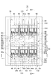
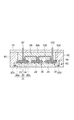
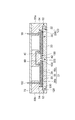
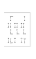
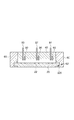
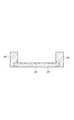
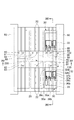
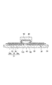
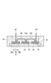
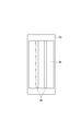
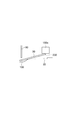
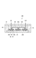
図1は、第1実施形態に係る半導体モジュールを模式的に示す平面図である。図2は、図1のII−II線に沿った半導体モジュールの断面図である。図3は、図1のIII−III線に沿った半導体モジュールの断面図である。図1において蓋70は便宜上表示されていない。
図6〜図21を参照しながら、本実施形態に係る半導体モジュールの製造方法の一例として、図1〜3に示される半導体モジュール10の製造方法について説明する。半導体モジュール10は例えば以下のようにして製造される。
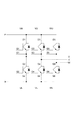
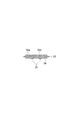
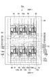
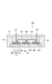
まず、図6〜図8に示されるように、回路基板30を準備する。回路基板30の凸部35は、例えば以下にようにして形成される。まず、絶縁基板33の主面とは反対側の面に設けられた金属層34上に金属膜を形成する。次に、フォトリソグラフィー法を用いて当該金属膜をエッチングすることによって凸部35を形成する。
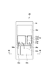
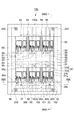
次に、図9〜図13に示されるように、ベース20に絶縁支持体40を取り付ける。絶縁支持体40は、ベース20の溝22に端子80〜91が対向配置されるように取り付けられ得る。絶縁支持体40は、樹脂中に端子80〜91を圧入し、樹脂を成型することにより形成される。また、ベース20に絶縁支持体60を取り付けてもよい。ベース20の溝22は、フォトリソグラフィー法を用いてベースをエッチングすることによって形成され得る。
次に、図14〜図16に示されるように、回路基板30をベース20に嵌め合わせる。回路基板30の凸部35が、ベース20の溝22に嵌め合わされ得る。例えば、凸部35が溝22に嵌め合わされた状態で、回路基板30をベース20の溝22に沿ってベース20の端部120から中央部220に向かってスライドさせることによって、端子80〜91とベース20との間に、回路基板30の第1の端部130を挿入する。これにより、半導体素子32の電極パッド36a,36b,36cが端子80〜91と接触して電気的に接続され得る。
次に、図17〜図20に示されるように、ベース20に絶縁支持体50a,50bを取り付ける。絶縁支持体50a,50bは、樹脂中に端子92〜102を圧入し、樹脂を成型することにより形成される。これにより、回路基板30の端部230がベース20に固定され得る。また、半導体素子32の電極パッド36a,36b,36cが端子92〜102と接触して電気的に接続され得る。
次に、図21に示されるように、蓋70を絶縁支持体40,50a,50b,60に貼り付ける。蓋70によって、ベース20及び絶縁支持体40,50a,50b,60によって囲まれた空間が封止される。
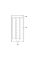
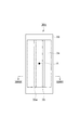
図22は、第2実施形態に係る半導体モジュールを模式的に示す平面図である。図23は、図22のXXIII−XXIII線に沿った半導体モジュールの断面図である。図24は、図22のXXIV−XXIV線に沿った半導体モジュールの断面図である。図22において蓋70は便宜上表示されていない。
図29は、第3実施形態に係る半導体モジュールを模式的に示す平面図である。図30は、図29のXXX−XXX線に沿った半導体モジュールの断面図である。図31は、図29のXXXI−XXXI線に沿った半導体モジュールの断面図である。図29において蓋70は便宜上表示されていない。
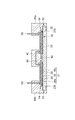
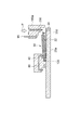
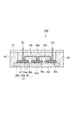
図34は、第4実施形態に係る半導体モジュールを模式的に示す断面図である。図34に示される半導体モジュール10cは、回路基板をベースに嵌め合わせるための構造が異なること以外は半導体モジュール10と同じ構成を備える。半導体モジュール10cは、回路基板30b及びベース20bを備える。
図37は、第5実施形態に係る半導体モジュールを模式的に示す断面図である。図37に示される半導体モジュール10dは、回路基板をベースに嵌め合わせるための構造が異なること以外は半導体モジュール10と同じ構成を備える。半導体モジュール10dは、回路基板30c及びベース20cを備える。回路基板30cは、金属層34に形成された凹部35aを備える。ベース20cは、凹部35aに対応する凸部22aを備える。
図38は、第6実施形態に係る半導体モジュールを模式的に示す断面図である。図38に示される半導体モジュール10eは、回路基板をベースに嵌め合わせるための構造が異なること以外は半導体モジュール10と同じ構成を備える。半導体モジュール10eは、回路基板30d及びベース20dを備える。回路基板30dは、凸部35及び凹部35aを備えていない。ベース20dは、回路基板30d全体に対応する溝22を備える。
図39は、第7実施形態に係る半導体モジュールを模式的に示す断面図である。図39に示される半導体モジュール10fは、回路基板をベースに嵌め合わせるための構造が異なること以外は半導体モジュール10と同じ構成を備える。半導体モジュール10fは、回路基板30e及びベース20eを備える。回路基板30eでは、凸部35の延在方向に垂直な断面形状が三角形になっている。このため、ベース20eでは、溝22の延在方向に垂直な断面形状も三角形になっている。
図40は、第8実施形態に係る半導体モジュールを模式的に示す断面図である。図40に示される半導体モジュール10gは、回路基板をベースに嵌め合わせるための構造が異なること以外は半導体モジュール10と同じ構成を備える。半導体モジュール10gは、回路基板30f及びベース20fを備える。回路基板30fでは、凸部35の延在方向に垂直な断面形状が半円になっている。このため、ベース20fでは、溝22の延在方向に垂直な断面形状も半円になっている。
Claims (9)
- ベースと、
少なくとも1つの回路基板と、
を備える半導体モジュールであって、
前記少なくとも1つの回路基板が、支持基板と前記支持基板によって支持される半導体素子とを有し、
前記ベースが、前記少なくとも1つの回路基板を前記ベースに嵌め合わせるための溝を有し、
前記溝が、前記溝の延在方向に沿って深くなっている、
半導体モジュール。 - 前記少なくとも1つの回路基板が複数の回路基板を備え、
前記複数の回路基板のそれぞれが、前記支持基板と前記半導体素子とを有する、請求項1に記載の半導体モジュール。 - 前記半導体素子と電気的に接続される端子を支持すると共に、前記ベースに取り付けられる絶縁支持体を更に備える、請求項1又は2に記載の半導体モジュール。
- 前記少なくとも1つの回路基板を前記ベースに固定する固定部材を更に備える、請求項1〜3のいずれか一項に記載の半導体モジュール。
- 前記少なくとも1つの回路基板の主面の中心を通ると共に前記主面に垂直な軸線に対して、前記溝が非対称に形成されている、請求項1〜4のいずれか一項に記載の半導体モジュール。
- 前記半導体素子がワイドバンドギャップ半導体を含む、請求項1〜5のいずれか一項に記載の半導体モジュール。
- 前記ワイドバンドギャップ半導体がSiC又はGaNである、請求項6に記載の半導体モジュール。
- 溝を有するベースに、前記溝に対向配置された端子を支持する絶縁支持体を取り付ける工程と、
前記端子と前記ベースとの間に、支持基板と前記支持基板によって支持される半導体素子とを有する回路基板の第1の端部を挿入する工程と、
前記回路基板の第1の端部とは異なる第2の端部を固定部材によって前記ベースに固定して、前記端子を前記半導体素子と電気的に接続すると共に、前記回路基板を前記ベースの前記溝に嵌め合わせる工程と、
を含む、半導体モジュールの製造方法。 - 前記溝が、前記溝の延在方向に沿って前記端子に向かって深くなっている、請求項8に記載の半導体モジュールの製造方法。
Priority Applications (2)
| Application Number | Priority Date | Filing Date | Title |
|---|---|---|---|
| JP2011241856A JP5716637B2 (ja) | 2011-11-04 | 2011-11-04 | 半導体モジュール及び半導体モジュールの製造方法 |
| US13/665,394 US8759839B2 (en) | 2011-11-04 | 2012-10-31 | Semiconductor module and method for manufacturing semiconductor module |
Applications Claiming Priority (1)
| Application Number | Priority Date | Filing Date | Title |
|---|---|---|---|
| JP2011241856A JP5716637B2 (ja) | 2011-11-04 | 2011-11-04 | 半導体モジュール及び半導体モジュールの製造方法 |
Publications (2)
| Publication Number | Publication Date |
|---|---|
| JP2013098450A JP2013098450A (ja) | 2013-05-20 |
| JP5716637B2 true JP5716637B2 (ja) | 2015-05-13 |
Family
ID=48223109
Family Applications (1)
| Application Number | Title | Priority Date | Filing Date |
|---|---|---|---|
| JP2011241856A Expired - Fee Related JP5716637B2 (ja) | 2011-11-04 | 2011-11-04 | 半導体モジュール及び半導体モジュールの製造方法 |
Country Status (2)
| Country | Link |
|---|---|
| US (1) | US8759839B2 (ja) |
| JP (1) | JP5716637B2 (ja) |
Families Citing this family (8)
| Publication number | Priority date | Publication date | Assignee | Title |
|---|---|---|---|---|
| JP6165025B2 (ja) * | 2013-10-31 | 2017-07-19 | 三菱電機株式会社 | 半導体モジュール |
| JP6308780B2 (ja) * | 2013-12-27 | 2018-04-11 | 三菱電機株式会社 | パワーモジュール |
| US10510642B2 (en) * | 2016-06-03 | 2019-12-17 | Mitsubishi Electric Corporation | Semiconductor device module |
| CN108738368B (zh) * | 2017-02-13 | 2022-06-17 | 新电元工业株式会社 | 电子设备 |
| US11109370B2 (en) * | 2017-03-21 | 2021-08-31 | Lg Electronics Inc. | Method for transmitting data in next generation communication system, and device therefor |
| JP7067255B2 (ja) * | 2018-05-16 | 2022-05-16 | 富士電機株式会社 | 半導体装置及び半導体装置の製造方法 |
| EP3989274A1 (en) * | 2020-10-23 | 2022-04-27 | SwissSEM Technologies AG | Power module |
| EP4336551B1 (en) * | 2022-09-09 | 2025-09-03 | Hitachi Energy Ltd | Power module comprising a semiconductor module component and an alignment part, and method for forming the power module |
Family Cites Families (14)
| Publication number | Priority date | Publication date | Assignee | Title |
|---|---|---|---|---|
| JPH02266557A (ja) * | 1989-04-06 | 1990-10-31 | Mitsubishi Electric Corp | 半導体装置 |
| JP2924498B2 (ja) | 1992-07-16 | 1999-07-26 | 富士電機株式会社 | 半導体装置 |
| JPH11214612A (ja) * | 1998-01-26 | 1999-08-06 | Hitachi Ltd | パワー半導体モジュール |
| JP2000031358A (ja) * | 1998-07-08 | 2000-01-28 | Sansha Electric Mfg Co Ltd | 電力用半導体モジュール |
| JP3919398B2 (ja) * | 1999-10-27 | 2007-05-23 | 三菱電機株式会社 | 半導体モジュール |
| JP2001168256A (ja) * | 1999-12-13 | 2001-06-22 | Sumitomo Electric Ind Ltd | 半導体素子用放熱構造体とそれを備えた半導体装置 |
| JP3972550B2 (ja) * | 2000-01-21 | 2007-09-05 | 三菱電機株式会社 | 電力用半導体装置 |
| JP4070470B2 (ja) * | 2002-01-24 | 2008-04-02 | 新光電気工業株式会社 | 半導体装置用多層回路基板及びその製造方法並びに半導体装置 |
| JP2004103936A (ja) * | 2002-09-11 | 2004-04-02 | Mitsubishi Electric Corp | 電力半導体装置およびその製造方法 |
| JP4991495B2 (ja) * | 2007-11-26 | 2012-08-01 | 東京エレクトロン株式会社 | 検査用保持部材及び検査用保持部材の製造方法 |
| JP2009188327A (ja) * | 2008-02-08 | 2009-08-20 | Toyota Motor Corp | パワーモジュールとその製造方法 |
| JP2011091088A (ja) * | 2009-10-20 | 2011-05-06 | Yaskawa Electric Corp | 発熱体の放熱構造、および該放熱構造を用いた半導体装置 |
| JP5574422B2 (ja) * | 2010-09-16 | 2014-08-20 | Fdkトワイセル株式会社 | 回路基板支持装置、該回路基板支持装置を備える電池ユニット |
| JP5383621B2 (ja) * | 2010-10-20 | 2014-01-08 | 三菱電機株式会社 | パワー半導体装置 |
-
2011
- 2011-11-04 JP JP2011241856A patent/JP5716637B2/ja not_active Expired - Fee Related
-
2012
- 2012-10-31 US US13/665,394 patent/US8759839B2/en active Active
Also Published As
| Publication number | Publication date |
|---|---|
| US20130112994A1 (en) | 2013-05-09 |
| US8759839B2 (en) | 2014-06-24 |
| JP2013098450A (ja) | 2013-05-20 |
Similar Documents
| Publication | Publication Date | Title |
|---|---|---|
| JP5716637B2 (ja) | 半導体モジュール及び半導体モジュールの製造方法 | |
| JP7352763B1 (ja) | 半導体モジュール | |
| JP7352753B2 (ja) | 半導体モジュール | |
| JP7382534B1 (ja) | 半導体モジュール | |
| US20110163432A1 (en) | Semiconductor device and method of manufacturing the same | |
| US20070290303A1 (en) | Dual leadframe semiconductor device package | |
| JP5924213B2 (ja) | 半導体モジュール | |
| JP5880127B2 (ja) | 半導体モジュールの製造方法及び半導体モジュールの製造装置 | |
| JP6065089B2 (ja) | 半導体モジュール |
Legal Events
| Date | Code | Title | Description |
|---|---|---|---|
| A621 | Written request for application examination |
Free format text: JAPANESE INTERMEDIATE CODE: A621 Effective date: 20140625 |
|
| A977 | Report on retrieval |
Free format text: JAPANESE INTERMEDIATE CODE: A971007 Effective date: 20141027 |
|
| A131 | Notification of reasons for refusal |
Free format text: JAPANESE INTERMEDIATE CODE: A131 Effective date: 20141118 |
|
| A521 | Request for written amendment filed |
Free format text: JAPANESE INTERMEDIATE CODE: A523 Effective date: 20150113 |
|
| TRDD | Decision of grant or rejection written | ||
| A01 | Written decision to grant a patent or to grant a registration (utility model) |
Free format text: JAPANESE INTERMEDIATE CODE: A01 Effective date: 20150217 |
|
| A61 | First payment of annual fees (during grant procedure) |
Free format text: JAPANESE INTERMEDIATE CODE: A61 Effective date: 20150302 |
|
| R150 | Certificate of patent or registration of utility model |
Ref document number: 5716637 Country of ref document: JP Free format text: JAPANESE INTERMEDIATE CODE: R150 |
|
| R250 | Receipt of annual fees |
Free format text: JAPANESE INTERMEDIATE CODE: R250 |
|
| R250 | Receipt of annual fees |
Free format text: JAPANESE INTERMEDIATE CODE: R250 |
|
| R250 | Receipt of annual fees |
Free format text: JAPANESE INTERMEDIATE CODE: R250 |
|
| R250 | Receipt of annual fees |
Free format text: JAPANESE INTERMEDIATE CODE: R250 |
|
| R250 | Receipt of annual fees |
Free format text: JAPANESE INTERMEDIATE CODE: R250 |
|
| R250 | Receipt of annual fees |
Free format text: JAPANESE INTERMEDIATE CODE: R250 |
|
| R250 | Receipt of annual fees |
Free format text: JAPANESE INTERMEDIATE CODE: R250 |
|
| LAPS | Cancellation because of no payment of annual fees |