JP5716637B2 - Semiconductor module and method for manufacturing semiconductor module - Google Patents

Semiconductor module and method for manufacturing semiconductor module Download PDF

Info

Publication number
JP5716637B2
JP5716637B2 JP2011241856A JP2011241856A JP5716637B2 JP 5716637 B2 JP5716637 B2 JP 5716637B2 JP 2011241856 A JP2011241856 A JP 2011241856A JP 2011241856 A JP2011241856 A JP 2011241856A JP 5716637 B2 JP5716637 B2 JP 5716637B2
Authority
JP
Japan
Prior art keywords
semiconductor module
base
circuit board
semiconductor
groove
Prior art date
Legal status (The legal status is an assumption and is not a legal conclusion. Google has not performed a legal analysis and makes no representation as to the accuracy of the status listed.)
Active
Application number
JP2011241856A
Other languages
Japanese (ja)
Other versions
JP2013098450A (en
Inventor
研一 澤田
研一 澤田
Current Assignee (The listed assignees may be inaccurate. Google has not performed a legal analysis and makes no representation or warranty as to the accuracy of the list.)
Sumitomo Electric Industries Ltd
Original Assignee
Sumitomo Electric Industries Ltd
Priority date (The priority date is an assumption and is not a legal conclusion. Google has not performed a legal analysis and makes no representation as to the accuracy of the date listed.)
Filing date
Publication date
Application filed by Sumitomo Electric Industries Ltd filed Critical Sumitomo Electric Industries Ltd
Priority to JP2011241856A priority Critical patent/JP5716637B2/en
Priority to US13/665,394 priority patent/US8759839B2/en
Publication of JP2013098450A publication Critical patent/JP2013098450A/en
Application granted granted Critical
Publication of JP5716637B2 publication Critical patent/JP5716637B2/en
Active legal-status Critical Current
Anticipated expiration legal-status Critical

Links

Images

Classifications

    • HELECTRICITY
    • H01ELECTRIC ELEMENTS
    • H01LSEMICONDUCTOR DEVICES NOT COVERED BY CLASS H10
    • H01L21/00Processes or apparatus adapted for the manufacture or treatment of semiconductor or solid state devices or of parts thereof
    • H01L21/02Manufacture or treatment of semiconductor devices or of parts thereof
    • H01L21/04Manufacture or treatment of semiconductor devices or of parts thereof the devices having at least one potential-jump barrier or surface barrier, e.g. PN junction, depletion layer or carrier concentration layer
    • H01L21/50Assembly of semiconductor devices using processes or apparatus not provided for in a single one of the subgroups H01L21/06 - H01L21/326, e.g. sealing of a cap to a base of a container
    • HELECTRICITY
    • H01ELECTRIC ELEMENTS
    • H01LSEMICONDUCTOR DEVICES NOT COVERED BY CLASS H10
    • H01L23/00Details of semiconductor or other solid state devices
    • H01L23/02Containers; Seals
    • H01L23/04Containers; Seals characterised by the shape of the container or parts, e.g. caps, walls
    • H01L23/043Containers; Seals characterised by the shape of the container or parts, e.g. caps, walls the container being a hollow construction and having a conductive base as a mounting as well as a lead for the semiconductor body
    • H01L23/049Containers; Seals characterised by the shape of the container or parts, e.g. caps, walls the container being a hollow construction and having a conductive base as a mounting as well as a lead for the semiconductor body the other leads being perpendicular to the base
    • HELECTRICITY
    • H01ELECTRIC ELEMENTS
    • H01LSEMICONDUCTOR DEVICES NOT COVERED BY CLASS H10
    • H01L25/00Assemblies consisting of a plurality of individual semiconductor or other solid state devices ; Multistep manufacturing processes thereof
    • H01L25/03Assemblies consisting of a plurality of individual semiconductor or other solid state devices ; Multistep manufacturing processes thereof all the devices being of a type provided for in the same subgroup of groups H01L27/00 - H01L33/00, or in a single subclass of H10K, H10N, e.g. assemblies of rectifier diodes
    • H01L25/04Assemblies consisting of a plurality of individual semiconductor or other solid state devices ; Multistep manufacturing processes thereof all the devices being of a type provided for in the same subgroup of groups H01L27/00 - H01L33/00, or in a single subclass of H10K, H10N, e.g. assemblies of rectifier diodes the devices not having separate containers
    • H01L25/07Assemblies consisting of a plurality of individual semiconductor or other solid state devices ; Multistep manufacturing processes thereof all the devices being of a type provided for in the same subgroup of groups H01L27/00 - H01L33/00, or in a single subclass of H10K, H10N, e.g. assemblies of rectifier diodes the devices not having separate containers the devices being of a type provided for in group H01L29/00
    • H01L25/072Assemblies consisting of a plurality of individual semiconductor or other solid state devices ; Multistep manufacturing processes thereof all the devices being of a type provided for in the same subgroup of groups H01L27/00 - H01L33/00, or in a single subclass of H10K, H10N, e.g. assemblies of rectifier diodes the devices not having separate containers the devices being of a type provided for in group H01L29/00 the devices being arranged next to each other
    • HELECTRICITY
    • H01ELECTRIC ELEMENTS
    • H01LSEMICONDUCTOR DEVICES NOT COVERED BY CLASS H10
    • H01L25/00Assemblies consisting of a plurality of individual semiconductor or other solid state devices ; Multistep manufacturing processes thereof
    • H01L25/18Assemblies consisting of a plurality of individual semiconductor or other solid state devices ; Multistep manufacturing processes thereof the devices being of types provided for in two or more different subgroups of the same main group of groups H01L27/00 - H01L33/00, or in a single subclass of H10K, H10N
    • HELECTRICITY
    • H01ELECTRIC ELEMENTS
    • H01LSEMICONDUCTOR DEVICES NOT COVERED BY CLASS H10
    • H01L2224/00Indexing scheme for arrangements for connecting or disconnecting semiconductor or solid-state bodies and methods related thereto as covered by H01L24/00
    • H01L2224/01Means for bonding being attached to, or being formed on, the surface to be connected, e.g. chip-to-package, die-attach, "first-level" interconnects; Manufacturing methods related thereto
    • H01L2224/26Layer connectors, e.g. plate connectors, solder or adhesive layers; Manufacturing methods related thereto
    • H01L2224/28Structure, shape, material or disposition of the layer connectors prior to the connecting process
    • H01L2224/29Structure, shape, material or disposition of the layer connectors prior to the connecting process of an individual layer connector
    • H01L2224/29001Core members of the layer connector
    • H01L2224/29099Material
    • H01L2224/291Material with a principal constituent of the material being a metal or a metalloid, e.g. boron [B], silicon [Si], germanium [Ge], arsenic [As], antimony [Sb], tellurium [Te] and polonium [Po], and alloys thereof
    • H01L2224/29101Material with a principal constituent of the material being a metal or a metalloid, e.g. boron [B], silicon [Si], germanium [Ge], arsenic [As], antimony [Sb], tellurium [Te] and polonium [Po], and alloys thereof the principal constituent melting at a temperature of less than 400°C
    • HELECTRICITY
    • H01ELECTRIC ELEMENTS
    • H01LSEMICONDUCTOR DEVICES NOT COVERED BY CLASS H10
    • H01L2224/00Indexing scheme for arrangements for connecting or disconnecting semiconductor or solid-state bodies and methods related thereto as covered by H01L24/00
    • H01L2224/01Means for bonding being attached to, or being formed on, the surface to be connected, e.g. chip-to-package, die-attach, "first-level" interconnects; Manufacturing methods related thereto
    • H01L2224/26Layer connectors, e.g. plate connectors, solder or adhesive layers; Manufacturing methods related thereto
    • H01L2224/31Structure, shape, material or disposition of the layer connectors after the connecting process
    • H01L2224/32Structure, shape, material or disposition of the layer connectors after the connecting process of an individual layer connector
    • H01L2224/321Disposition
    • H01L2224/32151Disposition the layer connector connecting between a semiconductor or solid-state body and an item not being a semiconductor or solid-state body, e.g. chip-to-substrate, chip-to-passive
    • H01L2224/32221Disposition the layer connector connecting between a semiconductor or solid-state body and an item not being a semiconductor or solid-state body, e.g. chip-to-substrate, chip-to-passive the body and the item being stacked
    • H01L2224/32225Disposition the layer connector connecting between a semiconductor or solid-state body and an item not being a semiconductor or solid-state body, e.g. chip-to-substrate, chip-to-passive the body and the item being stacked the item being non-metallic, e.g. insulating substrate with or without metallisation
    • HELECTRICITY
    • H01ELECTRIC ELEMENTS
    • H01LSEMICONDUCTOR DEVICES NOT COVERED BY CLASS H10
    • H01L2224/00Indexing scheme for arrangements for connecting or disconnecting semiconductor or solid-state bodies and methods related thereto as covered by H01L24/00
    • H01L2224/01Means for bonding being attached to, or being formed on, the surface to be connected, e.g. chip-to-package, die-attach, "first-level" interconnects; Manufacturing methods related thereto
    • H01L2224/42Wire connectors; Manufacturing methods related thereto
    • H01L2224/47Structure, shape, material or disposition of the wire connectors after the connecting process
    • H01L2224/48Structure, shape, material or disposition of the wire connectors after the connecting process of an individual wire connector
    • H01L2224/4805Shape
    • H01L2224/4809Loop shape
    • H01L2224/48091Arched
    • HELECTRICITY
    • H01ELECTRIC ELEMENTS
    • H01LSEMICONDUCTOR DEVICES NOT COVERED BY CLASS H10
    • H01L2224/00Indexing scheme for arrangements for connecting or disconnecting semiconductor or solid-state bodies and methods related thereto as covered by H01L24/00
    • H01L2224/01Means for bonding being attached to, or being formed on, the surface to be connected, e.g. chip-to-package, die-attach, "first-level" interconnects; Manufacturing methods related thereto
    • H01L2224/42Wire connectors; Manufacturing methods related thereto
    • H01L2224/47Structure, shape, material or disposition of the wire connectors after the connecting process
    • H01L2224/49Structure, shape, material or disposition of the wire connectors after the connecting process of a plurality of wire connectors
    • H01L2224/491Disposition
    • H01L2224/4911Disposition the connectors being bonded to at least one common bonding area, e.g. daisy chain
    • H01L2224/49113Disposition the connectors being bonded to at least one common bonding area, e.g. daisy chain the connectors connecting different bonding areas on the semiconductor or solid-state body to a common bonding area outside the body, e.g. converging wires
    • HELECTRICITY
    • H01ELECTRIC ELEMENTS
    • H01LSEMICONDUCTOR DEVICES NOT COVERED BY CLASS H10
    • H01L2224/00Indexing scheme for arrangements for connecting or disconnecting semiconductor or solid-state bodies and methods related thereto as covered by H01L24/00
    • H01L2224/73Means for bonding being of different types provided for in two or more of groups H01L2224/10, H01L2224/18, H01L2224/26, H01L2224/34, H01L2224/42, H01L2224/50, H01L2224/63, H01L2224/71
    • H01L2224/732Location after the connecting process
    • H01L2224/73251Location after the connecting process on different surfaces
    • H01L2224/73265Layer and wire connectors
    • HELECTRICITY
    • H01ELECTRIC ELEMENTS
    • H01LSEMICONDUCTOR DEVICES NOT COVERED BY CLASS H10
    • H01L23/00Details of semiconductor or other solid state devices
    • H01L23/34Arrangements for cooling, heating, ventilating or temperature compensation ; Temperature sensing arrangements
    • H01L23/36Selection of materials, or shaping, to facilitate cooling or heating, e.g. heatsinks
    • H01L23/373Cooling facilitated by selection of materials for the device or materials for thermal expansion adaptation, e.g. carbon
    • H01L23/3735Laminates or multilayers, e.g. direct bond copper ceramic substrates
    • HELECTRICITY
    • H01ELECTRIC ELEMENTS
    • H01LSEMICONDUCTOR DEVICES NOT COVERED BY CLASS H10
    • H01L23/00Details of semiconductor or other solid state devices
    • H01L23/34Arrangements for cooling, heating, ventilating or temperature compensation ; Temperature sensing arrangements
    • H01L23/42Fillings or auxiliary members in containers or encapsulations selected or arranged to facilitate heating or cooling
    • H01L23/433Auxiliary members in containers characterised by their shape, e.g. pistons
    • H01L23/4334Auxiliary members in encapsulations
    • HELECTRICITY
    • H01ELECTRIC ELEMENTS
    • H01LSEMICONDUCTOR DEVICES NOT COVERED BY CLASS H10
    • H01L24/00Arrangements for connecting or disconnecting semiconductor or solid-state bodies; Methods or apparatus related thereto
    • H01L24/01Means for bonding being attached to, or being formed on, the surface to be connected, e.g. chip-to-package, die-attach, "first-level" interconnects; Manufacturing methods related thereto
    • H01L24/26Layer connectors, e.g. plate connectors, solder or adhesive layers; Manufacturing methods related thereto
    • H01L24/28Structure, shape, material or disposition of the layer connectors prior to the connecting process
    • H01L24/29Structure, shape, material or disposition of the layer connectors prior to the connecting process of an individual layer connector
    • HELECTRICITY
    • H01ELECTRIC ELEMENTS
    • H01LSEMICONDUCTOR DEVICES NOT COVERED BY CLASS H10
    • H01L24/00Arrangements for connecting or disconnecting semiconductor or solid-state bodies; Methods or apparatus related thereto
    • H01L24/01Means for bonding being attached to, or being formed on, the surface to be connected, e.g. chip-to-package, die-attach, "first-level" interconnects; Manufacturing methods related thereto
    • H01L24/26Layer connectors, e.g. plate connectors, solder or adhesive layers; Manufacturing methods related thereto
    • H01L24/31Structure, shape, material or disposition of the layer connectors after the connecting process
    • H01L24/32Structure, shape, material or disposition of the layer connectors after the connecting process of an individual layer connector
    • HELECTRICITY
    • H01ELECTRIC ELEMENTS
    • H01LSEMICONDUCTOR DEVICES NOT COVERED BY CLASS H10
    • H01L24/00Arrangements for connecting or disconnecting semiconductor or solid-state bodies; Methods or apparatus related thereto
    • H01L24/01Means for bonding being attached to, or being formed on, the surface to be connected, e.g. chip-to-package, die-attach, "first-level" interconnects; Manufacturing methods related thereto
    • H01L24/42Wire connectors; Manufacturing methods related thereto
    • H01L24/47Structure, shape, material or disposition of the wire connectors after the connecting process
    • H01L24/48Structure, shape, material or disposition of the wire connectors after the connecting process of an individual wire connector
    • HELECTRICITY
    • H01ELECTRIC ELEMENTS
    • H01LSEMICONDUCTOR DEVICES NOT COVERED BY CLASS H10
    • H01L24/00Arrangements for connecting or disconnecting semiconductor or solid-state bodies; Methods or apparatus related thereto
    • H01L24/01Means for bonding being attached to, or being formed on, the surface to be connected, e.g. chip-to-package, die-attach, "first-level" interconnects; Manufacturing methods related thereto
    • H01L24/42Wire connectors; Manufacturing methods related thereto
    • H01L24/47Structure, shape, material or disposition of the wire connectors after the connecting process
    • H01L24/49Structure, shape, material or disposition of the wire connectors after the connecting process of a plurality of wire connectors
    • HELECTRICITY
    • H01ELECTRIC ELEMENTS
    • H01LSEMICONDUCTOR DEVICES NOT COVERED BY CLASS H10
    • H01L24/00Arrangements for connecting or disconnecting semiconductor or solid-state bodies; Methods or apparatus related thereto
    • H01L24/71Means for bonding not being attached to, or not being formed on, the surface to be connected
    • H01L24/72Detachable connecting means consisting of mechanical auxiliary parts connecting the device, e.g. pressure contacts using springs or clips
    • HELECTRICITY
    • H01ELECTRIC ELEMENTS
    • H01LSEMICONDUCTOR DEVICES NOT COVERED BY CLASS H10
    • H01L2924/00Indexing scheme for arrangements or methods for connecting or disconnecting semiconductor or solid-state bodies as covered by H01L24/00
    • H01L2924/0001Technical content checked by a classifier
    • H01L2924/00014Technical content checked by a classifier the subject-matter covered by the group, the symbol of which is combined with the symbol of this group, being disclosed without further technical details
    • HELECTRICITY
    • H01ELECTRIC ELEMENTS
    • H01LSEMICONDUCTOR DEVICES NOT COVERED BY CLASS H10
    • H01L2924/00Indexing scheme for arrangements or methods for connecting or disconnecting semiconductor or solid-state bodies as covered by H01L24/00
    • H01L2924/10Details of semiconductor or other solid state devices to be connected
    • H01L2924/102Material of the semiconductor or solid state bodies
    • H01L2924/1025Semiconducting materials
    • H01L2924/1026Compound semiconductors
    • H01L2924/1027IV
    • H01L2924/10272Silicon Carbide [SiC]
    • HELECTRICITY
    • H01ELECTRIC ELEMENTS
    • H01LSEMICONDUCTOR DEVICES NOT COVERED BY CLASS H10
    • H01L2924/00Indexing scheme for arrangements or methods for connecting or disconnecting semiconductor or solid-state bodies as covered by H01L24/00
    • H01L2924/10Details of semiconductor or other solid state devices to be connected
    • H01L2924/102Material of the semiconductor or solid state bodies
    • H01L2924/1025Semiconducting materials
    • H01L2924/1026Compound semiconductors
    • H01L2924/1032III-V
    • H01L2924/1033Gallium nitride [GaN]
    • HELECTRICITY
    • H01ELECTRIC ELEMENTS
    • H01LSEMICONDUCTOR DEVICES NOT COVERED BY CLASS H10
    • H01L2924/00Indexing scheme for arrangements or methods for connecting or disconnecting semiconductor or solid-state bodies as covered by H01L24/00
    • H01L2924/10Details of semiconductor or other solid state devices to be connected
    • H01L2924/11Device type
    • H01L2924/13Discrete devices, e.g. 3 terminal devices
    • H01L2924/1304Transistor
    • H01L2924/1305Bipolar Junction Transistor [BJT]
    • H01L2924/13055Insulated gate bipolar transistor [IGBT]
    • HELECTRICITY
    • H01ELECTRIC ELEMENTS
    • H01LSEMICONDUCTOR DEVICES NOT COVERED BY CLASS H10
    • H01L2924/00Indexing scheme for arrangements or methods for connecting or disconnecting semiconductor or solid-state bodies as covered by H01L24/00
    • H01L2924/10Details of semiconductor or other solid state devices to be connected
    • H01L2924/11Device type
    • H01L2924/13Discrete devices, e.g. 3 terminal devices
    • H01L2924/1304Transistor
    • H01L2924/1306Field-effect transistor [FET]
    • H01L2924/13091Metal-Oxide-Semiconductor Field-Effect Transistor [MOSFET]

Description

本発明は、半導体モジュール及び半導体モジュールの製造方法に関する。   The present invention relates to a semiconductor module and a method for manufacturing a semiconductor module.

半導体素子が搭載されたセラミックス基板と、当該セラミックス基板が取り付けられた金属ベースとを備える半導体モジュールが知られている(特許文献1参照)。   A semiconductor module including a ceramic substrate on which a semiconductor element is mounted and a metal base to which the ceramic substrate is attached is known (see Patent Document 1).

特開平6−85126号公報JP-A-6-85126

しかしながら、上述の半導体モジュールでは、半田等によりセラミックス基板を金属ベースに取り付ける際に、セラミックス基板が所望の位置からずれてしまうおそれがある。このため、セラミックス基板と金属ベースとの間の位置決め精度を向上させるのは容易でない。   However, in the above-described semiconductor module, when the ceramic substrate is attached to the metal base with solder or the like, the ceramic substrate may be displaced from a desired position. For this reason, it is not easy to improve the positioning accuracy between the ceramic substrate and the metal base.

本発明は、上記事情に鑑みて為されたものであり、半導体素子を有する回路基板とベースとの間において高い位置決め精度を有する半導体モジュール及び半導体モジュールの製造方法を提供することを目的とする。   The present invention has been made in view of the above circumstances, and an object thereof is to provide a semiconductor module having a high positioning accuracy between a circuit board having a semiconductor element and a base, and a method for manufacturing the semiconductor module.

上述の課題を解決するため、本発明の一側面に係る半導体モジュールは、ベースと、少なくとも1つの回路基板と、を備える半導体モジュールであって、前記少なくとも1つの回路基板が、支持基板と前記支持基板によって支持される半導体素子とを有し、前記ベース及び/又は前記支持基板が、前記少なくとも1つの回路基板を前記ベースに嵌め合わせるための構造を有する。   In order to solve the above-described problem, a semiconductor module according to one aspect of the present invention is a semiconductor module including a base and at least one circuit board, and the at least one circuit board includes a support substrate and the support. A semiconductor element supported by a substrate, and the base and / or the support substrate have a structure for fitting the at least one circuit board to the base.

この半導体モジュールでは、回路基板をベースに嵌め合わせることによって、回路基板とベースとの間において高い位置決め精度が得られる。   In this semiconductor module, a high positioning accuracy can be obtained between the circuit board and the base by fitting the circuit board to the base.

一実施形態において、半導体モジュールは、前記少なくとも1つの回路基板が複数の回路基板を備え、前記複数の回路基板のそれぞれが、前記支持基板と前記半導体素子とを有してもよい。   In one embodiment, in the semiconductor module, the at least one circuit board may include a plurality of circuit boards, and each of the plurality of circuit boards may include the support substrate and the semiconductor element.

半導体素子を支持基板に搭載する際に、実装によるストレスによって不良品の半導体素子が発生する可能性がある。半導体素子を直接検査することは困難であるため、通常、支持基板に搭載した後に半導体素子を検査する。ここで、複数の半導体素子が単一の支持基板によって支持されていると、検査により1つでも不良品の半導体素子が見つかると、支持基板によって支持された全ての半導体素子が無駄になってしまう。一方、上記半導体モジュールでは、個々の回路基板を検査して良品の回路基板を選別し、選別された良品の回路基板を選択的にベースに嵌め合わせることができる。このため、複数の半導体素子が単一の支持基板によって支持される場合に比べて、半導体モジュールの製造歩留まりを向上させることができる。   When a semiconductor element is mounted on a support substrate, a defective semiconductor element may be generated due to stress due to mounting. Since it is difficult to directly inspect a semiconductor element, the semiconductor element is usually inspected after being mounted on a support substrate. Here, when a plurality of semiconductor elements are supported by a single support substrate, if even one defective semiconductor element is found by inspection, all the semiconductor elements supported by the support substrate are wasted. . On the other hand, in the semiconductor module, each circuit board can be inspected to select a non-defective circuit board, and the selected non-defective circuit board can be selectively fitted to the base. For this reason, the manufacturing yield of a semiconductor module can be improved compared with the case where a plurality of semiconductor elements are supported by a single support substrate.

また、複数の半導体素子が単一の支持基板によって支持される場合、不良品の半導体素子が見つかった場合に備えて、良品の半導体素子を新たに搭載するためのスペースを支持基板に設けることがある。この場合、支持基板のサイズは大きくなる。一方、上記半導体モジュールでは、そのようなスペースが必要ないので、半導体モジュールを小型化できる。   Further, when a plurality of semiconductor elements are supported by a single support substrate, a space for newly mounting a non-defective semiconductor element may be provided on the support substrate in case a defective semiconductor element is found. is there. In this case, the size of the support substrate is increased. On the other hand, the semiconductor module does not require such a space, so that the semiconductor module can be reduced in size.

さらに、上記半導体モジュールでは、複数の半導体素子が単一の支持基板によって支持される場合に比べて、個々の回路基板のサイズを小さくすることができるので、回路基板が応力によって撓むことを抑制できる。   Furthermore, in the semiconductor module described above, the size of each circuit board can be reduced as compared with the case where a plurality of semiconductor elements are supported by a single support board, so that the circuit board is prevented from being bent by stress. it can.

一実施形態において、半導体モジュールは、前記半導体素子と電気的に接続される端子を支持すると共に、前記ベースに取り付けられる絶縁支持体を更に備えてもよい。   In one embodiment, the semiconductor module may further include an insulating support attached to the base while supporting a terminal electrically connected to the semiconductor element.

この場合、端子と絶縁支持体とが一体化しているので、半導体モジュールの組み立てが容易になる。   In this case, since the terminal and the insulating support are integrated, the assembly of the semiconductor module is facilitated.

一実施形態において、前記ベースが、前記構造として凹部又は凸部を有してもよい。   In one embodiment, the base may have a concave portion or a convex portion as the structure.

一実施形態において、前記ベースが、前記構造として溝を有してもよい。この場合、溝に沿って回路基板をスライドさせてベースに嵌め合わせることができるので、半導体モジュールの組み立てが容易になる。   In one embodiment, the base may have a groove as the structure. In this case, the circuit board can be slid along the groove and fitted to the base, so that the semiconductor module can be easily assembled.

一実施形態において、前記溝が、前記溝の延在方向に沿って深くなってもよい。この場合、溝が深くなっている部分に回路基板の端部を差し込み易くなるので、半導体モジュールの組み立てが容易になる。   In one embodiment, the groove may be deepened along the extending direction of the groove. In this case, since it becomes easy to insert the edge part of a circuit board in the part where the groove | channel is deep, the assembly of a semiconductor module becomes easy.

一実施形態において、半導体モジュールは、前記少なくとも1つの回路基板を前記ベースに固定する固定部材を更にてもよい。この場合、回路基板とベースとの間においてより高い位置決め精度が得られる。   In one embodiment, the semiconductor module may further include a fixing member that fixes the at least one circuit board to the base. In this case, higher positioning accuracy can be obtained between the circuit board and the base.

一実施形態において、前記少なくとも1つの回路基板の主面の中心を通ると共に前記主面に垂直な軸線に対して、前記構造が非対称に形成されてもよい。この場合、ベースに対する回路基板の向きが1つに決まるので、間違った向きで回路基板をベースに嵌め合わせることを抑制できる。その結果、半導体モジュールの組み立てが容易になる。   In one embodiment, the structure may be asymmetric with respect to an axis that passes through the center of the main surface of the at least one circuit board and is perpendicular to the main surface. In this case, since the direction of the circuit board with respect to the base is determined to be one, it is possible to suppress fitting of the circuit board to the base in the wrong direction. As a result, the assembly of the semiconductor module is facilitated.

一実施形態において、前記半導体素子がワイドバンドギャップ半導体を含んでもよい。前記ワイドバンドギャップ半導体がSiC又はGaNであってもよい。   In one embodiment, the semiconductor device may include a wide band gap semiconductor. The wide band gap semiconductor may be SiC or GaN.

本発明の一側面に係る半導体モジュールの製造方法は、支持基板と前記支持基板によって支持される半導体素子とを有する少なくとも1つの回路基板をベースに嵌め合わせる工程を含み、前記ベース及び/又は前記支持基板が、前記少なくとも1つの回路基板を前記ベースに嵌め合わせるための構造を有する。   The manufacturing method of the semiconductor module which concerns on 1 side of this invention includes the process of fitting at least 1 circuit board which has a support substrate and the semiconductor element supported by the said support substrate to a base, The said base and / or said support The board has a structure for fitting the at least one circuit board to the base.

この半導体モジュールの製造方法では、回路基板をベースに嵌め合わせることによって、回路基板とベースとの間において高い位置決め精度を有する半導体モジュールが得られる。   In this semiconductor module manufacturing method, a semiconductor module having high positioning accuracy between the circuit board and the base can be obtained by fitting the circuit board to the base.

本発明の別の側面に係る半導体モジュールの製造方法は、溝を有するベースに、前記溝に対向配置された端子を支持する絶縁支持体を取り付ける工程と、前記端子と前記ベースとの間に、支持基板と前記支持基板によって支持される半導体素子とを有する回路基板の第1の端部を挿入する工程と、前記回路基板の第1の端部とは異なる第2の端部を固定部材によって前記ベースに固定して、前記端子を前記半導体素子と電気的に接続すると共に、前記回路基板を前記ベースの前記溝に嵌め合わせる工程とを含む。   A method of manufacturing a semiconductor module according to another aspect of the present invention includes a step of attaching an insulating support that supports a terminal disposed opposite to the groove to a base having a groove, and between the terminal and the base, A step of inserting a first end of a circuit board having a support substrate and a semiconductor element supported by the support substrate; and a second end different from the first end of the circuit board by a fixing member Fixing to the base, electrically connecting the terminal to the semiconductor element, and fitting the circuit board into the groove of the base.

この半導体モジュールの製造方法では、回路基板をベースに嵌め合わせることによって、回路基板とベースとの間において高い位置決め精度を有する半導体モジュールが得られる。さらに、回路基板の第1の端部を端子とベースとの間に挿入する際に、端子が第1の端部を押圧することによって回路基板の反対側の端部が浮き上がってしまっても、固定部材によって回路基板をベースの溝に嵌め合わせることができる。   In this semiconductor module manufacturing method, a semiconductor module having high positioning accuracy between the circuit board and the base can be obtained by fitting the circuit board to the base. Furthermore, when the first end of the circuit board is inserted between the terminal and the base, even if the end on the opposite side of the circuit board is lifted by pressing the first end of the terminal, The circuit board can be fitted into the groove of the base by the fixing member.

一実施形態において、前記溝が、前記溝の延在方向に沿って前記端子に向かって深くなってもよい。   In one embodiment, the groove may become deeper toward the terminal along the extending direction of the groove.

この場合、端子と溝の底との間のスペースを広く維持することができるので、回路基板の第1の端部を斜めに挿入することができる。その結果、半導体モジュールの組み立てが容易になる。また、固定部材によってベースに第2の端部を固定する際に、てこの原理によって端子と半導体素子との間の電気的接続がより確実に得られる。   In this case, since the space between the terminal and the bottom of the groove can be kept wide, the first end of the circuit board can be inserted obliquely. As a result, the assembly of the semiconductor module is facilitated. Further, when the second end portion is fixed to the base by the fixing member, the electrical connection between the terminal and the semiconductor element is more reliably obtained by the lever principle.

本発明によれば、半導体素子を有する回路基板とベースとの間において高い位置決め精度を有する半導体モジュール及び半導体モジュールの製造方法が提供され得る。   ADVANTAGE OF THE INVENTION According to this invention, the manufacturing method of a semiconductor module which has high positioning accuracy between the circuit board which has a semiconductor element, and a base can be provided.

第1実施形態に係る半導体モジュールを模式的に示す平面図である。1 is a plan view schematically showing a semiconductor module according to a first embodiment. 図1のII−II線に沿った半導体モジュールの断面図である。It is sectional drawing of the semiconductor module along the II-II line | wire of FIG. 図1のIII−III線に沿った半導体モジュールの断面図である。It is sectional drawing of the semiconductor module along the III-III line | wire of FIG. 図1の半導体モジュールの等価回路結線図である。FIG. 2 is an equivalent circuit connection diagram of the semiconductor module of FIG. 1. 図1の半導体モジュールの端子の配置を模式的に示す図である。It is a figure which shows typically arrangement | positioning of the terminal of the semiconductor module of FIG. 図1の半導体モジュールを構成する回路基板を模式的に示す平面図である。It is a top view which shows typically the circuit board which comprises the semiconductor module of FIG. 図6の回路基板の裏面を模式的に示す平面図である。It is a top view which shows typically the back surface of the circuit board of FIG. 図6のVIII−VIII線に沿った回路基板の断面図である。It is sectional drawing of the circuit board along the VIII-VIII line of FIG. 第1実施形態に係る半導体モジュールの製造方法の一工程における構造体を模式的に示す平面図である。It is a top view which shows typically the structure in one process of the manufacturing method of the semiconductor module which concerns on 1st Embodiment. 図9のX−X線に沿った構造体の断面図である。It is sectional drawing of the structure along XX of FIG. 図9のXI−XI線に沿った構造体の断面図である。It is sectional drawing of the structure along the XI-XI line of FIG. 図9のXII−XII線に沿った構造体の断面図である。It is sectional drawing of the structure along the XII-XII line of FIG. 図9のXIII−XIII線に沿った構造体の断面図である。It is sectional drawing of the structure along the XIII-XIII line | wire of FIG. 第1実施形態に係る半導体モジュールの製造方法の一工程における構造体を模式的に示す平面図である。It is a top view which shows typically the structure in one process of the manufacturing method of the semiconductor module which concerns on 1st Embodiment. 図14のXV−XV線に沿った構造体の断面図である。It is sectional drawing of the structure along the XV-XV line | wire of FIG. 図14のXVI−XVI線に沿った構造体の断面図である。It is sectional drawing of the structure along the XVI-XVI line of FIG. 第1実施形態に係る半導体モジュールの製造方法の一工程における構造体を模式的に示す平面図である。It is a top view which shows typically the structure in one process of the manufacturing method of the semiconductor module which concerns on 1st Embodiment. 図17のXVIII−XVIII線に沿った構造体の断面図である。It is sectional drawing of the structure along the XVIII-XVIII line of FIG. 図17のXIX−XIX線に沿った構造体の断面図である。It is sectional drawing of the structure along the XIX-XIX line of FIG. 図17のXX−XX線に沿った構造体の断面図である。It is sectional drawing of the structure along the XX-XX line of FIG. 第1実施形態に係る半導体モジュールの蓋を模式的に示す平面図である。It is a top view which shows typically the cover of the semiconductor module which concerns on 1st Embodiment. 第2実施形態に係る半導体モジュールを模式的に示す平面図である。It is a top view which shows typically the semiconductor module which concerns on 2nd Embodiment. 図22のXXIII−XXIII線に沿った半導体モジュールの断面図である。FIG. 23 is a cross-sectional view of the semiconductor module along the line XXIII-XXIII in FIG. 22. 図22のXXIV−XXIV線に沿った半導体モジュールの断面図である。FIG. 23 is a cross-sectional view of the semiconductor module along the line XXIV-XXIV in FIG. 22. 図22の半導体モジュールの等価回路結線図である。FIG. 23 is an equivalent circuit connection diagram of the semiconductor module of FIG. 22. 図22の半導体モジュールを構成する回路基板を模式的に示す平面図である。It is a top view which shows typically the circuit board which comprises the semiconductor module of FIG. 図26の回路基板の裏面を模式的に示す平面図である。It is a top view which shows typically the back surface of the circuit board of FIG. 図26のXXVIII−XXVIII線に沿った回路基板の断面図である。It is sectional drawing of the circuit board along the XXVIII-XXVIII line | wire of FIG. 第3実施形態に係る半導体モジュールを模式的に示す平面図である。It is a top view which shows typically the semiconductor module which concerns on 3rd Embodiment. 図29のXXX−XXX線に沿った半導体モジュールの断面図である。FIG. 30 is a cross-sectional view of the semiconductor module along the line XXX-XXX in FIG. 29. 図29のXXXI−XXXI線に沿った半導体モジュールの断面図である。FIG. 30 is a cross-sectional view of the semiconductor module along the line XXXI-XXXI in FIG. 29. 第3実施形態に係る半導体モジュールの製造方法の一工程における構造体を模式的に示す図である。It is a figure which shows typically the structure in one process of the manufacturing method of the semiconductor module which concerns on 3rd Embodiment. 回路基板をベースに嵌め合わせるための構造の一例を示す図である。It is a figure which shows an example of the structure for fitting a circuit board to a base. 第4実施形態に係る半導体モジュールを模式的に示す断面図である。It is sectional drawing which shows typically the semiconductor module which concerns on 4th Embodiment. 図34の半導体モジュールを構成する回路基板を模式的に示す平面図である。FIG. 35 is a plan view schematically showing a circuit board constituting the semiconductor module of FIG. 34. 図35のXXXVI−XXXVI線に沿った回路基板の断面図である。FIG. 36 is a cross-sectional view of the circuit board along the line XXXVI-XXXVI in FIG. 35. 第5実施形態に係る半導体モジュールを模式的に示す断面図である。It is sectional drawing which shows typically the semiconductor module which concerns on 5th Embodiment. 第6実施形態に係る半導体モジュールを模式的に示す断面図である。It is sectional drawing which shows typically the semiconductor module which concerns on 6th Embodiment. 第7実施形態に係る半導体モジュールを模式的に示す断面図である。It is sectional drawing which shows typically the semiconductor module which concerns on 7th Embodiment. 第8実施形態に係る半導体モジュールを模式的に示す断面図である。It is sectional drawing which shows typically the semiconductor module which concerns on 8th Embodiment.

以下、添付図面を参照しながら本発明の実施形態を詳細に説明する。なお、図面の説明において、同一又は同等の要素には同一符号を用い、重複する説明を省略する。   Hereinafter, embodiments of the present invention will be described in detail with reference to the accompanying drawings. In the description of the drawings, the same reference numerals are used for the same or equivalent elements, and duplicate descriptions are omitted.

(第1実施形態)
<半導体モジュール>
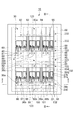
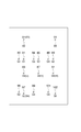
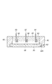
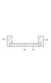
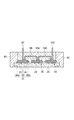
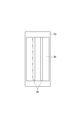
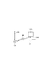
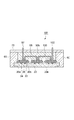
図1は、第1実施形態に係る半導体モジュールを模式的に示す平面図である。図2は、図1のII−II線に沿った半導体モジュールの断面図である。図3は、図1のIII−III線に沿った半導体モジュールの断面図である。図1において蓋70は便宜上表示されていない。
(First embodiment)
<Semiconductor module>
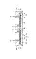
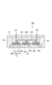
FIG. 1 is a plan view schematically showing the semiconductor module according to the first embodiment. FIG. 2 is a cross-sectional view of the semiconductor module taken along line II-II in FIG. FIG. 3 is a cross-sectional view of the semiconductor module taken along line III-III in FIG. In FIG. 1, the lid 70 is not displayed for convenience.

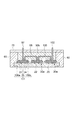
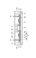
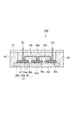
図1〜3に示される半導体モジュール10は、ベース20と、複数の回路基板30(本実施形態では例えば6つ)とを備える。複数の回路基板30は、ベース20上にアレイ配置され得る。半導体モジュール10は、単一の回路基板30を備えてもよい。複数の回路基板30のそれぞれは、支持基板31と支持基板31によって支持される半導体素子32とを有する(図6〜図8参照)。   1-3 includes a base 20 and a plurality of circuit boards 30 (for example, six in this embodiment). The plurality of circuit boards 30 can be arranged in an array on the base 20. The semiconductor module 10 may include a single circuit board 30. Each of the plurality of circuit boards 30 includes a support substrate 31 and a semiconductor element 32 supported by the support substrate 31 (see FIGS. 6 to 8).

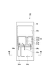
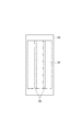
ベース20は、例えばCu、Al等の金属を含む金属ベースであり得る。ベース20は、放熱板として機能し得る。ベース20は、回路基板30をベース20に嵌め合わせるための構造として溝22を有してもよい。溝22は、ベース20の互いに対向する端部120からベース20の中央部220に向けて形成され得る。溝22は凹部であってもよい。   The base 20 may be a metal base including a metal such as Cu or Al. The base 20 can function as a heat sink. The base 20 may have a groove 22 as a structure for fitting the circuit board 30 to the base 20. The groove 22 may be formed from the mutually opposite end portions 120 of the base 20 toward the central portion 220 of the base 20. The groove 22 may be a recess.

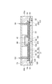
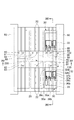
支持基板31は、絶縁基板33と、絶縁基板33の主面に設けられた電極パッド36a,36b,36cと、絶縁基板33の主面とは反対側の面に設けられた金属層34とを備え得る。絶縁基板33は例えばAlN、Al等のセラミックスを含む。電極パッド36a,36b,36c及び金属層34は、例えばCuを含む。金属層34上には、ベース20の溝22に嵌め合わされる凸部35が形成され得る。凸部35は、一方向に延在し得る。凸部35は、例えばCu等の金属を含む。凸部35の延在方向に垂直な断面形状は例えば矩形である。 The support substrate 31 includes an insulating substrate 33, electrode pads 36a, 36b, 36c provided on the main surface of the insulating substrate 33, and a metal layer 34 provided on the surface opposite to the main surface of the insulating substrate 33. Can be prepared. The insulating substrate 33 includes ceramics such as AlN and Al 2 O 3 . The electrode pads 36a, 36b, 36c and the metal layer 34 include, for example, Cu. On the metal layer 34, a convex portion 35 fitted into the groove 22 of the base 20 can be formed. The convex portion 35 can extend in one direction. The convex part 35 contains metals, such as Cu, for example. The cross-sectional shape perpendicular to the extending direction of the convex portion 35 is, for example, a rectangle.

半導体素子32は、例えば半導体チップである。半導体素子32は、ワイドバンドギャップ半導体を含む。この場合、シリコンに比べて半導体素子32の発生する熱量は大きくなるが、ベース20により放熱が適切に行われる。ワイドバンドギャップ半導体としては、例えばSiC又はGaN等の化合物半導体が挙げられる。このような場合、半導体素子32はパワー半導体素子として機能し得る。   The semiconductor element 32 is, for example, a semiconductor chip. The semiconductor element 32 includes a wide band gap semiconductor. In this case, although the amount of heat generated by the semiconductor element 32 is larger than that of silicon, the base 20 performs heat dissipation appropriately. Examples of the wide band gap semiconductor include a compound semiconductor such as SiC or GaN. In such a case, the semiconductor element 32 can function as a power semiconductor element.

半導体素子32は、トランジスタ32a及びダイオード32bを備え得る。トランジスタ32aとしては、例えばバイポーラトランジスタ、MOSFET、絶縁ゲートバイポーラトランジスタ(IGBT)等が挙げられる。トランジスタ32aは、半田37aを介して電極パッド36cに電気的に接続されている。ダイオード32bは、半田37bを介して電極パッド36cに電気的に接続されている。トランジスタ32aのゲートは、ワイヤ38aを介して電極パッド36aに電気的に接続されている。トランジスタ32aのソースは、ワイヤ38bを介して電極パッド36bに電気的に接続されている。ダイオード32bは、ワイヤ38cを介して電極パッド36bに電気的に接続されている。   The semiconductor element 32 may include a transistor 32a and a diode 32b. Examples of the transistor 32a include a bipolar transistor, a MOSFET, an insulated gate bipolar transistor (IGBT), and the like. The transistor 32a is electrically connected to the electrode pad 36c through the solder 37a. The diode 32b is electrically connected to the electrode pad 36c via the solder 37b. The gate of the transistor 32a is electrically connected to the electrode pad 36a through the wire 38a. The source of the transistor 32a is electrically connected to the electrode pad 36b through a wire 38b. The diode 32b is electrically connected to the electrode pad 36b through the wire 38c.

半導体モジュール10は、ベース20に取り付けられる絶縁支持体40を備えてもよい。絶縁支持体40は、ベース20の中央部220に取り付けられる。絶縁支持体40は、回路基板30の端部130(第1の端部)を把持する把持部42を有する。絶縁支持体40は、半導体素子32と電気的に接続される端子80〜91を支持する。端子80〜91は、ベース20上の回路基板30の端部130に向けて絶縁支持体40から突出している。   The semiconductor module 10 may include an insulating support 40 attached to the base 20. The insulating support 40 is attached to the central portion 220 of the base 20. The insulating support 40 has a grip portion 42 that grips the end portion 130 (first end portion) of the circuit board 30. The insulating support 40 supports the terminals 80 to 91 that are electrically connected to the semiconductor element 32. The terminals 80 to 91 protrude from the insulating support 40 toward the end portion 130 of the circuit board 30 on the base 20.

半導体モジュール10は、ベース20に取り付けられる絶縁支持体50a,50bを備えてもよい。絶縁支持体50a,50bは、ベース20の互いに対向する端部120にそれぞれ取り付けられる。絶縁支持体50a,50bのそれぞれは、ベース20の端部120を把持する把持部52と、回路基板30の端部230(第2の端部)を把持する把持部54とを有する。回路基板30の端部230は、溝22の延在方向に沿って端部130と反対側に位置する。絶縁支持体50aは、半導体素子32と電気的に接続される端子92〜95を支持する。端子92〜95は、ベース20上の回路基板30の端部230に向けて絶縁支持体50aから突出している。絶縁支持体50bは、半導体素子32と電気的に接続される端子96〜102を支持する。端子96〜102は、ベース20上の回路基板30の端部230に向けて絶縁支持体50bから突出している。   The semiconductor module 10 may include insulating supports 50 a and 50 b that are attached to the base 20. The insulating supports 50a and 50b are respectively attached to the end portions 120 of the base 20 facing each other. Each of the insulating supports 50a and 50b includes a grip portion 52 that grips the end portion 120 of the base 20, and a grip portion 54 that grips the end portion 230 (second end portion) of the circuit board 30. The end portion 230 of the circuit board 30 is located on the opposite side of the end portion 130 along the extending direction of the groove 22. The insulating support 50 a supports the terminals 92 to 95 that are electrically connected to the semiconductor element 32. The terminals 92 to 95 protrude from the insulating support 50 a toward the end 230 of the circuit board 30 on the base 20. The insulating support 50 b supports terminals 96 to 102 that are electrically connected to the semiconductor element 32. The terminals 96 to 102 protrude from the insulating support 50 b toward the end 230 of the circuit board 30 on the base 20.

半導体モジュール10は、ベース20に取り付けられる絶縁支持体60を備えてもよい。絶縁支持体60は、絶縁支持体40,50a,50bを挟むように、ベース20の互いに対向する側部320にそれぞれ取り付けられる。絶縁支持体60は、ベース20の互いに対向する側部320を把持する把持部62と、回路基板30の側部330を把持する把持部64とを有する。絶縁支持体60は、端子を支持していない。   The semiconductor module 10 may include an insulating support 60 attached to the base 20. The insulating support 60 is attached to the side portions 320 of the base 20 facing each other so as to sandwich the insulating supports 40, 50a, and 50b. The insulating support 60 includes a gripping portion 62 that grips the side portions 320 of the base 20 that face each other, and a gripping portion 64 that grips the side portion 330 of the circuit board 30. The insulating support 60 does not support the terminals.

絶縁支持体40,50a,50b,60は例えば樹脂を含む。端子80〜102は例えば金属ワイヤである。端子80〜102は、半導体素子32に直接接触(例えばスプリングコンタクト)してもよいし、ワイヤボンディング等により半導体素子32に接続されてもよい。   The insulating supports 40, 50a, 50b, 60 include, for example, a resin. The terminals 80 to 102 are, for example, metal wires. The terminals 80 to 102 may be in direct contact with the semiconductor element 32 (for example, spring contact), or may be connected to the semiconductor element 32 by wire bonding or the like.

端子80は、第1の半導体素子32の電極パッド36aに接続され、絶縁支持体40を貫通して半導体モジュール10の外部に突出する。端子81は、第1の半導体素子32の電極パッド36bに接続され、絶縁支持体40を貫通して半導体モジュール10の外部に突出する。端子82は、第1の半導体素子32の電極パッド36bに接続され、絶縁支持体40中を通って第2の半導体素子32の電極パッド36cに接続される。端子83は、第2の半導体素子32の電極パッド36aに接続され、絶縁支持体40を貫通して半導体モジュール10の外部に突出する。   The terminal 80 is connected to the electrode pad 36 a of the first semiconductor element 32, passes through the insulating support 40, and protrudes outside the semiconductor module 10. The terminal 81 is connected to the electrode pad 36 b of the first semiconductor element 32, passes through the insulating support 40, and protrudes outside the semiconductor module 10. The terminal 82 is connected to the electrode pad 36 b of the first semiconductor element 32, passes through the insulating support 40, and is connected to the electrode pad 36 c of the second semiconductor element 32. The terminal 83 is connected to the electrode pad 36 a of the second semiconductor element 32, passes through the insulating support 40, and protrudes outside the semiconductor module 10.

端子84は、第3の半導体素子32の電極パッド36aに接続され、絶縁支持体40を貫通して半導体モジュール10の外部に突出する。端子85は、第3の半導体素子32の電極パッド36bに接続され、絶縁支持体40を貫通して半導体モジュール10の外部に突出する。端子86は、第3の半導体素子32の電極パッド36bに接続され、絶縁支持体40中を通って第4の半導体素子32の電極パッド36cに接続される。端子87は、第4の半導体素子32の電極パッド36aに接続され、絶縁支持体40を貫通して半導体モジュール10の外部に突出する。   The terminal 84 is connected to the electrode pad 36 a of the third semiconductor element 32, penetrates through the insulating support 40, and protrudes outside the semiconductor module 10. The terminal 85 is connected to the electrode pad 36 b of the third semiconductor element 32, passes through the insulating support 40, and protrudes outside the semiconductor module 10. The terminal 86 is connected to the electrode pad 36 b of the third semiconductor element 32, passes through the insulating support 40, and is connected to the electrode pad 36 c of the fourth semiconductor element 32. The terminal 87 is connected to the electrode pad 36 a of the fourth semiconductor element 32, passes through the insulating support 40, and protrudes outside the semiconductor module 10.

端子88は、第5の半導体素子32の電極パッド36aに接続され、絶縁支持体40を貫通して半導体モジュール10の外部に突出する。端子89は、第5の半導体素子32の電極パッド36bに接続され、絶縁支持体40を貫通して半導体モジュール10の外部に突出する。端子90は、第5の半導体素子32の電極パッド36bに接続され、絶縁支持体40中を通って第6の半導体素子32の電極パッド36cに接続される。端子91は、第6の半導体素子32の電極パッド36aに接続され、絶縁支持体40を貫通して半導体モジュール10の外部に突出する。   The terminal 88 is connected to the electrode pad 36 a of the fifth semiconductor element 32 and protrudes outside the semiconductor module 10 through the insulating support 40. The terminal 89 is connected to the electrode pad 36 b of the fifth semiconductor element 32 and protrudes outside the semiconductor module 10 through the insulating support 40. The terminal 90 is connected to the electrode pad 36 b of the fifth semiconductor element 32, passes through the insulating support 40, and is connected to the electrode pad 36 c of the sixth semiconductor element 32. The terminal 91 is connected to the electrode pad 36 a of the sixth semiconductor element 32, passes through the insulating support 40, and protrudes outside the semiconductor module 10.

端子92は、第1の半導体素子32の電極パッド36cに接続され、絶縁支持体50aを貫通して半導体モジュール10の外部に突出する。端子93は、第1の半導体素子32の電極パッド36cに接続され、絶縁支持体50a中を通って第3の半導体素子32の電極パッド36cに接続される。端子94は、第3の半導体素子32の電極パッド36cに接続され、絶縁支持体50a中を通って第5の半導体素子32の電極パッド36cに接続される。端子95は、第5の半導体素子32の電極パッド36cに接続され、絶縁支持体50aを貫通して半導体モジュール10の外部に突出する。   The terminal 92 is connected to the electrode pad 36c of the first semiconductor element 32, penetrates through the insulating support 50a, and protrudes outside the semiconductor module 10. The terminal 93 is connected to the electrode pad 36c of the first semiconductor element 32, and is connected to the electrode pad 36c of the third semiconductor element 32 through the insulating support 50a. The terminal 94 is connected to the electrode pad 36c of the third semiconductor element 32, and is connected to the electrode pad 36c of the fifth semiconductor element 32 through the insulating support 50a. The terminal 95 is connected to the electrode pad 36c of the fifth semiconductor element 32, penetrates through the insulating support 50a, and protrudes outside the semiconductor module 10.

端子96は、第2の半導体素子32の電極パッド36aに接続され、絶縁支持体50bを貫通して半導体モジュール10の外部に突出する。端子97は、第2の半導体素子32の電極パッド36bに接続され、絶縁支持体50bを貫通して半導体モジュール10の外部に突出する。端子98は、第2の半導体素子32の電極パッド36bに接続され、絶縁支持体50b中を通って第4の半導体素子32の電極パッド36bに接続される。端子99は、第4の半導体素子32の電極パッド36aに接続され、絶縁支持体50bを貫通して半導体モジュール10の外部に突出する。端子100は、第4の半導体素子32の電極パッド36bに接続され、絶縁支持体50b中を通って第6の半導体素子32の電極パッド36bに接続される。端子101は、第6の半導体素子32の電極パッド36aに接続され、絶縁支持体50bを貫通して半導体モジュール10の外部に突出する。端子102は、第6の半導体素子32の電極パッド36bに接続され、絶縁支持体50bを貫通して半導体モジュール10の外部に突出する。   The terminal 96 is connected to the electrode pad 36 a of the second semiconductor element 32 and protrudes outside the semiconductor module 10 through the insulating support 50 b. The terminal 97 is connected to the electrode pad 36b of the second semiconductor element 32, passes through the insulating support 50b, and protrudes outside the semiconductor module 10. The terminal 98 is connected to the electrode pad 36b of the second semiconductor element 32, and is connected to the electrode pad 36b of the fourth semiconductor element 32 through the insulating support 50b. The terminal 99 is connected to the electrode pad 36 a of the fourth semiconductor element 32 and protrudes outside the semiconductor module 10 through the insulating support 50 b. The terminal 100 is connected to the electrode pad 36b of the fourth semiconductor element 32, and is connected to the electrode pad 36b of the sixth semiconductor element 32 through the insulating support 50b. The terminal 101 is connected to the electrode pad 36a of the sixth semiconductor element 32, protrudes outside the semiconductor module 10 through the insulating support 50b. The terminal 102 is connected to the electrode pad 36b of the sixth semiconductor element 32, protrudes outside the semiconductor module 10 through the insulating support 50b.

半導体モジュール10は、絶縁支持体40,50a,50b,60上に配置されると共にベース20に対向配置される蓋70を更に備えてもよい。蓋70には、端子80,81,83,84,85,87,88,89,91,92,95,96,97,99,101,102通る貫通孔が形成され得る。蓋70は例えば樹脂を含む。   The semiconductor module 10 may further include a lid 70 that is disposed on the insulating supports 40, 50 a, 50 b, 60 and is disposed to face the base 20. The lid 70 may be formed with a through hole through which the terminals 80, 81, 83, 84, 85, 87, 88, 89, 91, 92, 95, 96, 97, 99, 101, 102 pass. The lid 70 includes, for example, a resin.

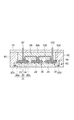
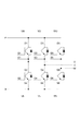
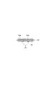
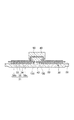
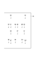
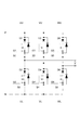
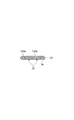
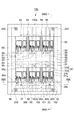
図4は、図1の半導体モジュールの等価回路結線図である。図5は、図1の半導体モジュールの端子の配置を模式的に示す図である。図4及び図5に示されるように、半導体モジュール10は、U相、V相及びW相を有する3相インバータ用モジュールとして機能し得る。各回路基板30において、トランジスタ32aはダイオード32bと逆並列接続されている。   FIG. 4 is an equivalent circuit connection diagram of the semiconductor module of FIG. FIG. 5 is a diagram schematically showing the arrangement of terminals of the semiconductor module of FIG. As shown in FIGS. 4 and 5, the semiconductor module 10 can function as a three-phase inverter module having a U phase, a V phase, and a W phase. In each circuit board 30, the transistor 32a is connected in antiparallel with the diode 32b.

半導体モジュール10では、回路基板30をベース20に嵌め合わせることによって、回路基板30とベース20との間において高い位置決め精度が得られる。   In the semiconductor module 10, high positioning accuracy can be obtained between the circuit board 30 and the base 20 by fitting the circuit board 30 to the base 20.

半導体素子を支持基板に搭載する際に、実装(ダイシング、ダイボンディング、ワイヤボンディング等)によるストレスによって不良品の半導体素子が発生する可能性がある。半導体素子を直接検査することは困難であるため、通常、支持基板に搭載した後に半導体素子を検査する。ここで、複数の半導体素子が単一の支持基板によって支持されていると、検査により1つでも不良品の半導体素子が見つかると、支持基板によって支持された全ての半導体素子が無駄になってしまう。一方、半導体モジュール10では、個々の回路基板30を検査して良品の回路基板30を選別し、選別された良品の回路基板30を選択的にベース20に嵌め合わせることができる。このため、複数の半導体素子が単一の支持基板によって支持される場合に比べて、半導体モジュール10の製造歩留まりを向上させることができる。   When a semiconductor element is mounted on a support substrate, a defective semiconductor element may be generated due to stress due to mounting (dicing, die bonding, wire bonding, etc.). Since it is difficult to directly inspect a semiconductor element, the semiconductor element is usually inspected after being mounted on a support substrate. Here, when a plurality of semiconductor elements are supported by a single support substrate, if even one defective semiconductor element is found by inspection, all the semiconductor elements supported by the support substrate are wasted. . On the other hand, in the semiconductor module 10, individual circuit boards 30 can be inspected to select non-defective circuit boards 30, and the selected non-defective circuit boards 30 can be selectively fitted to the base 20. For this reason, the manufacturing yield of the semiconductor module 10 can be improved compared with the case where a plurality of semiconductor elements are supported by a single support substrate.

また、複数の半導体素子が単一の支持基板によって支持される場合、不良品の半導体素子が見つかった場合に備えて、良品の半導体素子を新たに搭載するためのスペースを支持基板に設けることがある。この場合、支持基板のサイズは大きくなる。一方、半導体モジュール10では、複数の回路基板30のそれぞれが支持基板31と半導体素子32とを有している。そのため、良品の半導体素子を新たに搭載するためのスペースが必要ないので、半導体モジュール10を小型化できる。さらに、半導体モジュール10では、複数の半導体素子が単一の支持基板によって支持される場合に比べて、個々の回路基板30のサイズを小さくすることができるので、回路基板30が応力によって撓むことを抑制できる。   Further, when a plurality of semiconductor elements are supported by a single support substrate, a space for newly mounting a non-defective semiconductor element may be provided on the support substrate in case a defective semiconductor element is found. is there. In this case, the size of the support substrate is increased. On the other hand, in the semiconductor module 10, each of the plurality of circuit boards 30 includes a support substrate 31 and a semiconductor element 32. This eliminates the need for a space for newly mounting a non-defective semiconductor element, thereby reducing the size of the semiconductor module 10. Furthermore, in the semiconductor module 10, since the size of each circuit board 30 can be reduced as compared with the case where a plurality of semiconductor elements are supported by a single support board, the circuit board 30 bends due to stress. Can be suppressed.

半導体モジュール10が、端子80〜91を支持する絶縁支持体40を備える場合、端子80〜91と絶縁支持体40とが一体化しているので、半導体モジュール10の組み立てが容易になる。   When the semiconductor module 10 includes the insulating support body 40 that supports the terminals 80 to 91, the terminals 80 to 91 and the insulating support body 40 are integrated, so that the assembly of the semiconductor module 10 is facilitated.

半導体モジュール10が、溝22を有するベース20を備える場合、溝22に沿って回路基板30をスライドさせてベース20に嵌め合わせることができるので、半導体モジュール10の組み立てが容易になる。   When the semiconductor module 10 includes the base 20 having the groove 22, the circuit board 30 can be slid along the groove 22 and fitted to the base 20, so that the assembly of the semiconductor module 10 is facilitated.

<半導体モジュールの製造方法>
図6〜図21を参照しながら、本実施形態に係る半導体モジュールの製造方法の一例として、図1〜3に示される半導体モジュール10の製造方法について説明する。半導体モジュール10は例えば以下のようにして製造される。
<Semiconductor module manufacturing method>
With reference to FIGS. 6 to 21, a method for manufacturing the semiconductor module 10 shown in FIGS. 1 to 3 will be described as an example of a method for manufacturing the semiconductor module according to the present embodiment. The semiconductor module 10 is manufactured as follows, for example.

(回路基板の準備工程)
まず、図6〜図8に示されるように、回路基板30を準備する。回路基板30の凸部35は、例えば以下にようにして形成される。まず、絶縁基板33の主面とは反対側の面に設けられた金属層34上に金属膜を形成する。次に、フォトリソグラフィー法を用いて当該金属膜をエッチングすることによって凸部35を形成する。
(Circuit board preparation process)
First, as shown in FIGS. 6 to 8, a circuit board 30 is prepared. The convex portion 35 of the circuit board 30 is formed as follows, for example. First, a metal film is formed on the metal layer 34 provided on the surface opposite to the main surface of the insulating substrate 33. Next, the convex portion 35 is formed by etching the metal film using a photolithography method.

回路基板30は、必要に応じて電気試験等によって検査され得る。検査により、良品の回路基板30が選別される。   The circuit board 30 can be inspected by an electrical test or the like as necessary. The non-defective circuit board 30 is selected by the inspection.

(第1の絶縁支持体の取り付け工程)
次に、図9〜図13に示されるように、ベース20に絶縁支持体40を取り付ける。絶縁支持体40は、ベース20の溝22に端子80〜91が対向配置されるように取り付けられ得る。絶縁支持体40は、樹脂中に端子80〜91を圧入し、樹脂を成型することにより形成される。また、ベース20に絶縁支持体60を取り付けてもよい。ベース20の溝22は、フォトリソグラフィー法を用いてベースをエッチングすることによって形成され得る。
(Attaching process of first insulating support)
Next, as shown in FIGS. 9 to 13, the insulating support 40 is attached to the base 20. The insulating support body 40 can be attached so that the terminals 80 to 91 are opposed to the groove 22 of the base 20. The insulating support 40 is formed by press-fitting terminals 80 to 91 into a resin and molding the resin. Further, the insulating support 60 may be attached to the base 20. The groove 22 of the base 20 can be formed by etching the base using a photolithography method.

(回路基板の嵌め合わせ工程)
次に、図14〜図16に示されるように、回路基板30をベース20に嵌め合わせる。回路基板30の凸部35が、ベース20の溝22に嵌め合わされ得る。例えば、凸部35が溝22に嵌め合わされた状態で、回路基板30をベース20の溝22に沿ってベース20の端部120から中央部220に向かってスライドさせることによって、端子80〜91とベース20との間に、回路基板30の第1の端部130を挿入する。これにより、半導体素子32の電極パッド36a,36b,36cが端子80〜91と接触して電気的に接続され得る。
(Circuit board fitting process)
Next, as shown in FIGS. 14 to 16, the circuit board 30 is fitted to the base 20. The convex portion 35 of the circuit board 30 can be fitted into the groove 22 of the base 20. For example, by sliding the circuit board 30 from the end portion 120 of the base 20 toward the central portion 220 along the groove 22 of the base 20 with the convex portion 35 fitted in the groove 22, the terminals 80 to 91 and The first end 130 of the circuit board 30 is inserted between the base 20 and the base 20. Thereby, the electrode pads 36a, 36b, and 36c of the semiconductor element 32 can be brought into contact with and electrically connected to the terminals 80 to 91.

(第2の絶縁支持体の取り付け工程)
次に、図17〜図20に示されるように、ベース20に絶縁支持体50a,50bを取り付ける。絶縁支持体50a,50bは、樹脂中に端子92〜102を圧入し、樹脂を成型することにより形成される。これにより、回路基板30の端部230がベース20に固定され得る。また、半導体素子32の電極パッド36a,36b,36cが端子92〜102と接触して電気的に接続され得る。
(Second insulating support attachment step)
Next, as shown in FIGS. 17 to 20, the insulating supports 50 a and 50 b are attached to the base 20. The insulating supports 50a and 50b are formed by press-fitting terminals 92 to 102 into a resin and molding the resin. Thereby, the end portion 230 of the circuit board 30 can be fixed to the base 20. Also, the electrode pads 36a, 36b, 36c of the semiconductor element 32 can be in contact with and electrically connected to the terminals 92-102.

(蓋の貼り付け工程)
次に、図21に示されるように、蓋70を絶縁支持体40,50a,50b,60に貼り付ける。蓋70によって、ベース20及び絶縁支持体40,50a,50b,60によって囲まれた空間が封止される。
(Cover pasting process)
Next, as shown in FIG. 21, the lid 70 is attached to the insulating supports 40, 50 a, 50 b, 60. The space surrounded by the base 20 and the insulating supports 40, 50a, 50b, 60 is sealed by the lid 70.

なお、上記各工程の順序を入れ替えてもよいし、複数の工程を同時に行ってもよい。例えば、第1の絶縁支持体の取り付け工程の前に回路基板の嵌め合わせ工程を行ってもよい。また、第1の絶縁支持体の取り付け工程の後に回路基板の準備工程を行ってもよい。また、回路基板の嵌め合わせ工程と第2の絶縁支持体の取り付け工程とを同時に行ってもよい。   In addition, the order of each said process may be replaced and a several process may be performed simultaneously. For example, a circuit board fitting process may be performed before the first insulating support mounting process. Moreover, you may perform the preparation process of a circuit board after the attachment process of a 1st insulating support body. Further, the circuit board fitting step and the second insulating support attaching step may be performed simultaneously.

上記半導体モジュールの製造方法では、回路基板30をベース20に嵌め合わせることによって、回路基板30とベース20との間において高い位置決め精度を有する半導体モジュール10が得られる。   In the semiconductor module manufacturing method, the semiconductor module 10 having high positioning accuracy between the circuit board 30 and the base 20 is obtained by fitting the circuit board 30 to the base 20.

(第2実施形態)
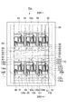
図22は、第2実施形態に係る半導体モジュールを模式的に示す平面図である。図23は、図22のXXIII−XXIII線に沿った半導体モジュールの断面図である。図24は、図22のXXIV−XXIV線に沿った半導体モジュールの断面図である。図22において蓋70は便宜上表示されていない。
(Second Embodiment)
FIG. 22 is a plan view schematically showing a semiconductor module according to the second embodiment. 23 is a cross-sectional view of the semiconductor module taken along line XXIII-XXIII in FIG. FIG. 24 is a cross-sectional view of the semiconductor module taken along line XXIV-XXIV in FIG. In FIG. 22, the lid 70 is not displayed for convenience.

図22〜23に示される半導体モジュール10aは、回路基板30に代えて回路基板30aを備えること以外は半導体モジュール10と同じ構成を備える。回路基板30aは、支持基板131と支持基板131によって支持される半導体素子132とを有する(図26〜図28参照)。   The semiconductor module 10 a shown in FIGS. 22 to 23 has the same configuration as the semiconductor module 10 except that the circuit board 30 a is provided instead of the circuit board 30. The circuit board 30a includes a support substrate 131 and a semiconductor element 132 supported by the support substrate 131 (see FIGS. 26 to 28).

支持基板131は、絶縁基板33と、絶縁基板33の主面に設けられた電極パッド136a,136b,136c,136dと、絶縁基板33の主面とは反対側の面に設けられた金属層34とを備え得る。   The support substrate 131 includes an insulating substrate 33, electrode pads 136 a, 136 b, 136 c, and 136 d provided on the main surface of the insulating substrate 33, and a metal layer 34 provided on the surface opposite to the main surface of the insulating substrate 33. Can be provided.

半導体素子132は、トランジスタ132a、ダイオード132b及びダイオード132cを備え得る。トランジスタ132aは、半田137aを介して電極パッド136cに電気的に接続されている。ダイオード132bは、半田137bを介して電極パッド136cに電気的に接続されている。トランジスタ132aのゲートは、ワイヤ138aを介して電極パッド136aに電気的に接続されている。ダイオード132cは、半田137cを介して電極パッド136dに電気的に接続されている。トランジスタ132aのソースは、ワイヤ138bを介して電極パッド136bに電気的に接続されている。ダイオード132bは、ワイヤ138cを介して電極パッド136dに電気的に接続されている。ダイオード132cは、ワイヤ138dを介して電極パッド136bに電気的に接続されている。   The semiconductor element 132 may include a transistor 132a, a diode 132b, and a diode 132c. The transistor 132a is electrically connected to the electrode pad 136c through the solder 137a. The diode 132b is electrically connected to the electrode pad 136c through the solder 137b. The gate of the transistor 132a is electrically connected to the electrode pad 136a through the wire 138a. The diode 132c is electrically connected to the electrode pad 136d through the solder 137c. The source of the transistor 132a is electrically connected to the electrode pad 136b through a wire 138b. The diode 132b is electrically connected to the electrode pad 136d through the wire 138c. The diode 132c is electrically connected to the electrode pad 136b through the wire 138d.

図25は、図22の半導体モジュールの等価回路結線図である。半導体モジュール10aの端子の配置は、図5に示される半導体モジュール10の端子の配置と同じである。図5及び図25に示されるように、半導体モジュール10aは、U相、V相及びW相を有する3相インバータ用モジュールとして機能し得る。各回路基板30において、トランジスタ132aはMOSFETであり、ダイオード132bはトランジスタ132aに直列接続され、ダイオード132cはトランジスタ132a及びダイオード132bの両端に逆並列接続される。ダイオード132bはMOSFET中の寄生ダイオードの動作を抑制し得る。   FIG. 25 is an equivalent circuit connection diagram of the semiconductor module of FIG. The arrangement of the terminals of the semiconductor module 10a is the same as the arrangement of the terminals of the semiconductor module 10 shown in FIG. As shown in FIGS. 5 and 25, the semiconductor module 10a can function as a three-phase inverter module having a U phase, a V phase, and a W phase. In each circuit board 30, the transistor 132a is a MOSFET, the diode 132b is connected in series to the transistor 132a, and the diode 132c is connected in antiparallel to both ends of the transistor 132a and the diode 132b. The diode 132b can suppress the operation of the parasitic diode in the MOSFET.

半導体モジュール10aでは、半導体モジュール10と同様の作用効果が得られる。また、半導体モジュール10aは、半導体モジュール10の製造方法と同様の方法によって製造され得る。   In the semiconductor module 10a, the same effects as the semiconductor module 10 can be obtained. Further, the semiconductor module 10 a can be manufactured by a method similar to the method for manufacturing the semiconductor module 10.

(第3実施形態)
図29は、第3実施形態に係る半導体モジュールを模式的に示す平面図である。図30は、図29のXXX−XXX線に沿った半導体モジュールの断面図である。図31は、図29のXXXI−XXXI線に沿った半導体モジュールの断面図である。図29において蓋70は便宜上表示されていない。
(Third embodiment)
FIG. 29 is a plan view schematically showing a semiconductor module according to the third embodiment. FIG. 30 is a cross-sectional view of the semiconductor module taken along line XXX-XXX in FIG. FIG. 31 is a cross-sectional view of the semiconductor module along the line XXXI-XXXI in FIG. In FIG. 29, the lid 70 is not displayed for convenience.

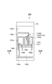
図29〜31に示される半導体モジュール10bは、絶縁支持体50a,50bに代えて絶縁支持体150a,150bを備え、ベース20に代えてベース20aを備え、固定部材としてのねじ200を更に備えること以外は半導体モジュール10と同じ構成を備える。   A semiconductor module 10b shown in FIGS. 29 to 31 includes insulating supports 150a and 150b instead of the insulating supports 50a and 50b, a base 20a instead of the base 20, and a screw 200 as a fixing member. Except for the above, the semiconductor module 10 has the same configuration.

ベース20aは、ねじ孔24を更に備えること以外はベース20と同じ構成を備える。 絶縁支持体150a,150bは、把持部52を備えておらず、ねじ200が貫通していること以外は絶縁支持体50a,50bと同じ構成を備える。   The base 20 a has the same configuration as the base 20 except that the base 20 a further includes a screw hole 24. The insulating supports 150a and 150b do not include the grip portion 52 and have the same configuration as the insulating supports 50a and 50b except that the screw 200 passes therethrough.

ねじ200は、回路基板30をベース20aに固定する。ねじ200は、絶縁支持体150a,150bを介して、回路基板30の端部230をベース20aに固定する。ねじ200は、ベース20のコーナーにおいて、絶縁支持体150a,150bを通ってベース20aのねじ孔24に取り付けられている。   The screw 200 fixes the circuit board 30 to the base 20a. The screw 200 fixes the end 230 of the circuit board 30 to the base 20a via the insulating supports 150a and 150b. The screw 200 is attached to the screw hole 24 of the base 20a at the corner of the base 20 through the insulating supports 150a and 150b.

半導体モジュール10bでは、半導体モジュール10と同様の作用効果が得られる。また、半導体モジュール10bは、半導体モジュール10の製造方法と同様の方法によって製造され得る。本実施形態では、回路基板の嵌め合わせ工程と第2の絶縁支持体の取り付け工程とが同時に行われる。   In the semiconductor module 10b, the same effect as the semiconductor module 10 can be obtained. The semiconductor module 10b can be manufactured by a method similar to the method for manufacturing the semiconductor module 10. In the present embodiment, the circuit board fitting process and the second insulating support mounting process are performed simultaneously.

まず、凸部35が溝22に嵌め合わされた状態で、回路基板30をベース20の溝22に沿ってベース20の端部120から中央部220に向かってスライドさせることによって、端子80〜91とベース20との間に、回路基板30の第1の端部130を挿入する。その後、図32に示されるように、絶縁支持体150a,150bを圧力Pによってベース20aに押圧し、ねじ200をねじ孔24に取り付けることによって、回路基板30の端部230をベース20aに固定する。これにより、端子80〜91を半導体素子32と電気的に接続すると共に、回路基板30をベース20aの溝22に嵌め合わせる。   First, in a state where the convex portion 35 is fitted in the groove 22, the circuit board 30 is slid along the groove 22 of the base 20 from the end portion 120 of the base 20 toward the central portion 220. The first end 130 of the circuit board 30 is inserted between the base 20 and the base 20. Thereafter, as shown in FIG. 32, the end portions 230 of the circuit board 30 are fixed to the base 20a by pressing the insulating supports 150a and 150b against the base 20a with the pressure P and attaching the screws 200 to the screw holes 24. . Thereby, the terminals 80 to 91 are electrically connected to the semiconductor element 32, and the circuit board 30 is fitted into the groove 22 of the base 20a.

半導体モジュール10bの製造方法では、回路基板30の端部130を端子80〜91とベース20aとの間に挿入する際に、図32に示されるように、端子80〜91が端部130を押圧することによって回路基板30の端部230が浮き上がってしまっても、ねじ200によって回路基板30をベース20aの溝22に嵌め合わせることができる。   In the manufacturing method of the semiconductor module 10b, when the end portion 130 of the circuit board 30 is inserted between the terminals 80 to 91 and the base 20a, the terminals 80 to 91 press the end portion 130 as shown in FIG. As a result, even if the end 230 of the circuit board 30 is lifted, the circuit board 30 can be fitted into the groove 22 of the base 20a by the screw 200.

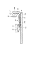
溝22は、図33に示されるように、溝22の延在方向に沿って深くなってもよい。溝22は、溝22の全体又は一部において、溝22の延在方向に沿って徐々に深くなってもよいし、溝22の延在方向に沿って階段状に深くなってもよい。溝22は、端子80〜91に向かって深くなっている。この場合、端子80〜91と溝22の底との間のスペースを広く維持することができるので、回路基板30の端部130を斜めに挿入することができる。その結果、半導体モジュール10bの組み立てが容易になる。また、ねじ200によってベース20aに回路基板30の端部230を固定する際に、てこの原理によって端子80〜91と半導体素子32との間の電気的接続がより確実に得られる。   As shown in FIG. 33, the groove 22 may be deepened along the extending direction of the groove 22. The groove 22 may be gradually deepened along the extending direction of the groove 22 in the whole or a part of the groove 22, or may be deepened stepwise along the extending direction of the groove 22. The groove 22 is deeper toward the terminals 80 to 91. In this case, since the space between the terminals 80 to 91 and the bottom of the groove 22 can be maintained wide, the end portion 130 of the circuit board 30 can be inserted obliquely. As a result, the assembly of the semiconductor module 10b is facilitated. Further, when the end portion 230 of the circuit board 30 is fixed to the base 20a with the screw 200, the electrical connection between the terminals 80 to 91 and the semiconductor element 32 can be obtained more reliably by the lever principle.

なお、固定部材として、ねじ200に代えて例えば接着剤を用いてもよい。   For example, an adhesive may be used as the fixing member instead of the screw 200.

(第4実施形態)
図34は、第4実施形態に係る半導体モジュールを模式的に示す断面図である。図34に示される半導体モジュール10cは、回路基板をベースに嵌め合わせるための構造が異なること以外は半導体モジュール10と同じ構成を備える。半導体モジュール10cは、回路基板30b及びベース20bを備える。
(Fourth embodiment)
FIG. 34 is a cross-sectional view schematically showing a semiconductor module according to the fourth embodiment. The semiconductor module 10c shown in FIG. 34 has the same configuration as the semiconductor module 10 except that the structure for fitting the circuit board to the base is different. The semiconductor module 10c includes a circuit board 30b and a base 20b.

回路基板30bは、凹部35a及び凸部35を備えること以外は回路基板30と同じ構成を備える(図35〜図36参照)。凹部35a及び凸部35は、回路基板30bの主面の中心(例えば重心)を通ると共に主面に垂直な軸線Aの両側に配置されている。回路基板30bをベース20bに嵌め合わせるための構造は、軸線Aに対して非対称に形成されている。凹部35aは金属層34をエッチングすることにより形成され得る。ベース20bは、凸部35に嵌め合わされる溝22に加えて、凹部35aに嵌め合わされる凸部22aを有する。凸部22aは、ベースをエッチングすることにより形成され得る。   The circuit board 30b has the same configuration as the circuit board 30 except that the circuit board 30b includes the concave portions 35a and the convex portions 35 (see FIGS. 35 to 36). The concave portion 35a and the convex portion 35 are disposed on both sides of the axis A that passes through the center (for example, the center of gravity) of the main surface of the circuit board 30b and is perpendicular to the main surface. The structure for fitting the circuit board 30b to the base 20b is asymmetric with respect to the axis A. The recess 35 a can be formed by etching the metal layer 34. In addition to the groove 22 fitted into the convex part 35, the base 20b has a convex part 22a fitted into the concave part 35a. The convex portion 22a can be formed by etching the base.

半導体モジュール10cでは、半導体モジュール10と同様の作用効果が得られる。また、半導体モジュール10cは、半導体モジュール10の製造方法と同様の方法によって製造され得る。さらに、半導体モジュール10cでは、ベース20bに対する回路基板30bの向きが1つに決まるので、間違った向きで回路基板30bをベース20bに嵌め合わせることを抑制できる。その結果、半導体モジュール10cの組み立てが容易になる。   In the semiconductor module 10c, the same effects as the semiconductor module 10 can be obtained. Further, the semiconductor module 10 c can be manufactured by a method similar to the method for manufacturing the semiconductor module 10. Furthermore, in the semiconductor module 10c, since the direction of the circuit board 30b with respect to the base 20b is determined as one, it is possible to suppress the circuit board 30b from being fitted to the base 20b in the wrong direction. As a result, the assembly of the semiconductor module 10c is facilitated.

(第5実施形態)
図37は、第5実施形態に係る半導体モジュールを模式的に示す断面図である。図37に示される半導体モジュール10dは、回路基板をベースに嵌め合わせるための構造が異なること以外は半導体モジュール10と同じ構成を備える。半導体モジュール10dは、回路基板30c及びベース20cを備える。回路基板30cは、金属層34に形成された凹部35aを備える。ベース20cは、凹部35aに対応する凸部22aを備える。
(Fifth embodiment)
FIG. 37 is a cross-sectional view schematically showing a semiconductor module according to the fifth embodiment. The semiconductor module 10d shown in FIG. 37 has the same configuration as the semiconductor module 10 except that the structure for fitting the circuit board to the base is different. The semiconductor module 10d includes a circuit board 30c and a base 20c. The circuit board 30 c includes a recess 35 a formed in the metal layer 34. The base 20c includes a convex portion 22a corresponding to the concave portion 35a.

半導体モジュール10dでは、半導体モジュール10と同様の作用効果が得られる。また、半導体モジュール10dは、半導体モジュール10の製造方法と同様の方法によって製造され得る。   In the semiconductor module 10d, the same effects as the semiconductor module 10 can be obtained. The semiconductor module 10d can be manufactured by a method similar to the method for manufacturing the semiconductor module 10.

(第6実施形態)
図38は、第6実施形態に係る半導体モジュールを模式的に示す断面図である。図38に示される半導体モジュール10eは、回路基板をベースに嵌め合わせるための構造が異なること以外は半導体モジュール10と同じ構成を備える。半導体モジュール10eは、回路基板30d及びベース20dを備える。回路基板30dは、凸部35及び凹部35aを備えていない。ベース20dは、回路基板30d全体に対応する溝22を備える。
(Sixth embodiment)
FIG. 38 is a cross-sectional view schematically showing a semiconductor module according to the sixth embodiment. The semiconductor module 10e shown in FIG. 38 has the same configuration as the semiconductor module 10 except that the structure for fitting the circuit board to the base is different. The semiconductor module 10e includes a circuit board 30d and a base 20d. The circuit board 30d does not include the convex portion 35 and the concave portion 35a. The base 20d includes a groove 22 corresponding to the entire circuit board 30d.

半導体モジュール10eでは、半導体モジュール10と同様の作用効果が得られる。また、半導体モジュール10eは、半導体モジュール10の製造方法と同様の方法によって製造され得る。   In the semiconductor module 10e, the same effects as the semiconductor module 10 can be obtained. Further, the semiconductor module 10e can be manufactured by a method similar to the method for manufacturing the semiconductor module 10.

(第7実施形態)
図39は、第7実施形態に係る半導体モジュールを模式的に示す断面図である。図39に示される半導体モジュール10fは、回路基板をベースに嵌め合わせるための構造が異なること以外は半導体モジュール10と同じ構成を備える。半導体モジュール10fは、回路基板30e及びベース20eを備える。回路基板30eでは、凸部35の延在方向に垂直な断面形状が三角形になっている。このため、ベース20eでは、溝22の延在方向に垂直な断面形状も三角形になっている。
(Seventh embodiment)
FIG. 39 is a cross-sectional view schematically showing a semiconductor module according to the seventh embodiment. The semiconductor module 10f shown in FIG. 39 has the same configuration as the semiconductor module 10 except that the structure for fitting the circuit board to the base is different. The semiconductor module 10f includes a circuit board 30e and a base 20e. In the circuit board 30e, the cross-sectional shape perpendicular to the extending direction of the convex portion 35 is a triangle. For this reason, in the base 20e, the cross-sectional shape perpendicular to the extending direction of the groove 22 is also a triangle.

半導体モジュール10fでは、半導体モジュール10と同様の作用効果が得られる。また、半導体モジュール10fは、半導体モジュール10の製造方法と同様の方法によって製造され得る。   In the semiconductor module 10f, the same effects as the semiconductor module 10 can be obtained. Further, the semiconductor module 10 f can be manufactured by a method similar to the method for manufacturing the semiconductor module 10.

(第8実施形態)
図40は、第8実施形態に係る半導体モジュールを模式的に示す断面図である。図40に示される半導体モジュール10gは、回路基板をベースに嵌め合わせるための構造が異なること以外は半導体モジュール10と同じ構成を備える。半導体モジュール10gは、回路基板30f及びベース20fを備える。回路基板30fでは、凸部35の延在方向に垂直な断面形状が半円になっている。このため、ベース20fでは、溝22の延在方向に垂直な断面形状も半円になっている。
(Eighth embodiment)
FIG. 40 is a cross-sectional view schematically showing a semiconductor module according to the eighth embodiment. A semiconductor module 10g shown in FIG. 40 has the same configuration as the semiconductor module 10 except that the structure for fitting the circuit board to the base is different. The semiconductor module 10g includes a circuit board 30f and a base 20f. In the circuit board 30f, the cross-sectional shape perpendicular to the extending direction of the convex portion 35 is a semicircle. For this reason, in the base 20f, the cross-sectional shape perpendicular to the extending direction of the groove 22 is also a semicircle.

半導体モジュール10gでは、半導体モジュール10と同様の作用効果が得られる。また、半導体モジュール10gは、半導体モジュール10の製造方法と同様の方法によって製造され得る。   In the semiconductor module 10g, the same effects as the semiconductor module 10 can be obtained. The semiconductor module 10g can be manufactured by a method similar to the method for manufacturing the semiconductor module 10.

以上、本発明の好適な実施形態について詳細に説明したが、本発明は上記各実施形態に限定されない。第1〜第8実施形態に係る半導体モジュールの各構成は、互いに組み合わされてもよい。ベースが凹部を有し、支持基板が凹部に対応する凸部を有してもよい。ベースが凸部を有し、支持基板が凸部に対応する凹部を有してもよい。ベースが凹部を有し、支持基板が凹部にそのまま嵌め合わされてもよい。回路基板をベースに嵌め合わせるための構造は、任意の形状を有する凹部、溝、凸部、レール等であってもよい。   As mentioned above, although preferred embodiment of this invention was described in detail, this invention is not limited to said each embodiment. The components of the semiconductor modules according to the first to eighth embodiments may be combined with each other. The base may have a recess, and the support substrate may have a protrusion corresponding to the recess. The base may have a convex portion, and the support substrate may have a concave portion corresponding to the convex portion. The base may have a recess, and the support substrate may be directly fitted into the recess. The structure for fitting the circuit board to the base may be a concave portion, groove, convex portion, rail or the like having an arbitrary shape.

10,10a、10b、10c,10d,10e,10f,10g…半導体モジュール、20,20a、20b,20c,20d,20e,20f…ベース、22…溝(回路基板をベースに嵌め合わせるための構造)、30,30a、30b,30c,30d,30e,30f…回路基板、31,131…支持基板、32,132…半導体素子、40…絶縁支持体、80〜91…端子、130…回路基板の第1の端部、200…ねじ(固定部材)、230…回路基板の第2の端部、A…軸線。   10, 10a, 10b, 10c, 10d, 10e, 10f, 10g... Semiconductor module, 20, 20a, 20b, 20c, 20d, 20e, 20f... Base, 22 .. groove (structure for fitting the circuit board to the base) 30, 30 a, 30 b, 30 c, 30 d, 30 e, 30 f... Circuit board, 31, 131 ... support substrate, 32, 132 ... semiconductor element, 40 ... insulating support, 80 to 91 ... terminal, 130 ... 1 end, 200... Screw (fixing member), 230... Second end of circuit board, A.

Claims (9)

ベースと、
少なくとも1つの回路基板と、
を備える半導体モジュールであって、
前記少なくとも1つの回路基板が、支持基板と前記支持基板によって支持される半導体素子とを有し、
前記ベースが、前記少なくとも1つの回路基板を前記ベースに嵌め合わせるためのを有し、
前記溝が、前記溝の延在方向に沿って深くなっている、
半導体モジュール。
Base and
At least one circuit board;
A semiconductor module comprising:
The at least one circuit board includes a support substrate and a semiconductor element supported by the support substrate;
The base is, have a groove for fitting the said at least one circuit board to the base,
The groove is deeper along the extending direction of the groove,
Semiconductor module.
前記少なくとも1つの回路基板が複数の回路基板を備え、
前記複数の回路基板のそれぞれが、前記支持基板と前記半導体素子とを有する、請求項1に記載の半導体モジュール。
The at least one circuit board comprises a plurality of circuit boards;
The semiconductor module according to claim 1, wherein each of the plurality of circuit boards includes the support substrate and the semiconductor element.
前記半導体素子と電気的に接続される端子を支持すると共に、前記ベースに取り付けられる絶縁支持体を更に備える、請求項1又は2に記載の半導体モジュール。   The semiconductor module according to claim 1, further comprising an insulating support body that supports a terminal electrically connected to the semiconductor element and is attached to the base. 前記少なくとも1つの回路基板を前記ベースに固定する固定部材を更に備える、請求項1〜のいずれか一項に記載の半導体モジュール。 Wherein the at least further comprising one circuit board fixing member for fixing to the base, the semiconductor module according to any one of claims 1-3. 前記少なくとも1つの回路基板の主面の中心を通ると共に前記主面に垂直な軸線に対して、前記が非対称に形成されている、請求項1〜のいずれか一項に記載の半導体モジュール。 The semiconductor module according to relative axis normal to said major surface, said grooves are formed asymmetrically, to any one of claims 1 to 4 together through the center of the main surface of the at least one circuit board . 前記半導体素子がワイドバンドギャップ半導体を含む、請求項1〜のいずれか一項に記載の半導体モジュール。 The semiconductor device includes a wide band gap semiconductor, the semiconductor module according to any one of claims 1-5. 前記ワイドバンドギャップ半導体がSiC又はGaNである、請求項に記載の半導体モジュール。 The semiconductor module according to claim 6 , wherein the wide band gap semiconductor is SiC or GaN. 溝を有するベースに、前記溝に対向配置された端子を支持する絶縁支持体を取り付ける工程と、
前記端子と前記ベースとの間に、支持基板と前記支持基板によって支持される半導体素子とを有する回路基板の第1の端部を挿入する工程と、
前記回路基板の第1の端部とは異なる第2の端部を固定部材によって前記ベースに固定して、前記端子を前記半導体素子と電気的に接続すると共に、前記回路基板を前記ベースの前記溝に嵌め合わせる工程と、
を含む、半導体モジュールの製造方法。
Attaching a base having a groove to an insulating support that supports a terminal disposed opposite to the groove; and
Inserting a first end of a circuit board having a support substrate and a semiconductor element supported by the support substrate between the terminal and the base;
A second end different from the first end of the circuit board is fixed to the base by a fixing member, the terminal is electrically connected to the semiconductor element, and the circuit board is connected to the base of the base. Fitting the groove,
A method for manufacturing a semiconductor module, comprising:
前記溝が、前記溝の延在方向に沿って前記端子に向かって深くなっている、請求項に記載の半導体モジュールの製造方法。
The method of manufacturing a semiconductor module according to claim 8 , wherein the groove is deeper toward the terminal along the extending direction of the groove.
JP2011241856A 2011-11-04 2011-11-04 Semiconductor module and method for manufacturing semiconductor module Active JP5716637B2 (en)

Priority Applications (2)

Application Number Priority Date Filing Date Title
JP2011241856A JP5716637B2 (en) 2011-11-04 2011-11-04 Semiconductor module and method for manufacturing semiconductor module
US13/665,394 US8759839B2 (en) 2011-11-04 2012-10-31 Semiconductor module and method for manufacturing semiconductor module

Applications Claiming Priority (1)

Application Number Priority Date Filing Date Title
JP2011241856A JP5716637B2 (en) 2011-11-04 2011-11-04 Semiconductor module and method for manufacturing semiconductor module

Publications (2)

Publication Number Publication Date
JP2013098450A JP2013098450A (en) 2013-05-20
JP5716637B2 true JP5716637B2 (en) 2015-05-13

Family

ID=48223109

Family Applications (1)

Application Number Title Priority Date Filing Date
JP2011241856A Active JP5716637B2 (en) 2011-11-04 2011-11-04 Semiconductor module and method for manufacturing semiconductor module

Country Status (2)

Country Link
US (1) US8759839B2 (en)
JP (1) JP5716637B2 (en)

Families Citing this family (7)

* Cited by examiner, † Cited by third party
Publication number Priority date Publication date Assignee Title
JP6165025B2 (en) * 2013-10-31 2017-07-19 三菱電機株式会社 Semiconductor module
JP6308780B2 (en) * 2013-12-27 2018-04-11 三菱電機株式会社 Power module
CN109196641B (en) * 2016-06-03 2021-10-29 三菱电机株式会社 Semiconductor device module
JP6496845B2 (en) * 2017-02-13 2019-04-10 新電元工業株式会社 Electronics
WO2018174555A1 (en) * 2017-03-21 2018-09-27 엘지전자 주식회사 Method for transmitting data in next generation communication system, and device therefor
JP7067255B2 (en) * 2018-05-16 2022-05-16 富士電機株式会社 Semiconductor devices and methods for manufacturing semiconductor devices
EP3989274A1 (en) * 2020-10-23 2022-04-27 SwissSEM Technologies AG Power module

Family Cites Families (14)

* Cited by examiner, † Cited by third party
Publication number Priority date Publication date Assignee Title
JPH02266557A (en) * 1989-04-06 1990-10-31 Mitsubishi Electric Corp Semiconductor device
JP2924498B2 (en) 1992-07-16 1999-07-26 富士電機株式会社 Semiconductor device
JPH11214612A (en) * 1998-01-26 1999-08-06 Hitachi Ltd Power semiconductor module
JP2000031358A (en) * 1998-07-08 2000-01-28 Sansha Electric Mfg Co Ltd Power semiconductor module
JP3919398B2 (en) * 1999-10-27 2007-05-23 三菱電機株式会社 Semiconductor module
JP2001168256A (en) * 1999-12-13 2001-06-22 Sumitomo Electric Ind Ltd Heat dissipation structure for semiconductor component and semiconductor device provided with that
JP3972550B2 (en) * 2000-01-21 2007-09-05 三菱電機株式会社 Power semiconductor device
JP4070470B2 (en) * 2002-01-24 2008-04-02 新光電気工業株式会社 Multilayer circuit board for semiconductor device, manufacturing method thereof, and semiconductor device
JP2004103936A (en) * 2002-09-11 2004-04-02 Mitsubishi Electric Corp Power semiconductor device and manufacturing method thereof
JP4991495B2 (en) * 2007-11-26 2012-08-01 東京エレクトロン株式会社 Inspection holding member and manufacturing method of inspection holding member
JP2009188327A (en) * 2008-02-08 2009-08-20 Toyota Motor Corp Power module and its manufacturing method
JP2011091088A (en) * 2009-10-20 2011-05-06 Yaskawa Electric Corp Heat radiation structure of heating element and semiconductor device using the heat radiation structure
JP5574422B2 (en) * 2010-09-16 2014-08-20 Fdkトワイセル株式会社 Circuit board support device and battery unit including the circuit board support device
JP5383621B2 (en) * 2010-10-20 2014-01-08 三菱電機株式会社 Power semiconductor device

Also Published As

Publication number Publication date
US8759839B2 (en) 2014-06-24
US20130112994A1 (en) 2013-05-09
JP2013098450A (en) 2013-05-20

Similar Documents

Publication Publication Date Title
JP5716637B2 (en) Semiconductor module and method for manufacturing semiconductor module
JP7352753B2 (en) semiconductor module
JP7352763B1 (en) semiconductor module
JP7354475B1 (en) semiconductor module
US20130256920A1 (en) Semiconductor device
US20110163432A1 (en) Semiconductor device and method of manufacturing the same
US20230245956A1 (en) Semiconductor module
JP5924213B2 (en) Semiconductor module
JP5880127B2 (en) Semiconductor module manufacturing method and semiconductor module manufacturing apparatus
JP6065089B2 (en) Semiconductor module
US20230253335A1 (en) Semiconductor module and semiconductor module manufacturing method
WO2022080072A1 (en) Semiconductor module

Legal Events

Date Code Title Description
A621 Written request for application examination

Free format text: JAPANESE INTERMEDIATE CODE: A621

Effective date: 20140625

A977 Report on retrieval

Free format text: JAPANESE INTERMEDIATE CODE: A971007

Effective date: 20141027

A131 Notification of reasons for refusal

Free format text: JAPANESE INTERMEDIATE CODE: A131

Effective date: 20141118

A521 Request for written amendment filed

Free format text: JAPANESE INTERMEDIATE CODE: A523

Effective date: 20150113

TRDD Decision of grant or rejection written
A01 Written decision to grant a patent or to grant a registration (utility model)

Free format text: JAPANESE INTERMEDIATE CODE: A01

Effective date: 20150217

A61 First payment of annual fees (during grant procedure)

Free format text: JAPANESE INTERMEDIATE CODE: A61

Effective date: 20150302

R150 Certificate of patent or registration of utility model

Ref document number: 5716637

Country of ref document: JP

Free format text: JAPANESE INTERMEDIATE CODE: R150

R250 Receipt of annual fees

Free format text: JAPANESE INTERMEDIATE CODE: R250

R250 Receipt of annual fees

Free format text: JAPANESE INTERMEDIATE CODE: R250

R250 Receipt of annual fees

Free format text: JAPANESE INTERMEDIATE CODE: R250

R250 Receipt of annual fees

Free format text: JAPANESE INTERMEDIATE CODE: R250

R250 Receipt of annual fees

Free format text: JAPANESE INTERMEDIATE CODE: R250

R250 Receipt of annual fees

Free format text: JAPANESE INTERMEDIATE CODE: R250

R250 Receipt of annual fees

Free format text: JAPANESE INTERMEDIATE CODE: R250