JP5692949B2 - 露光装置 - Google Patents
露光装置 Download PDFInfo
- Publication number
- JP5692949B2 JP5692949B2 JP2006322518A JP2006322518A JP5692949B2 JP 5692949 B2 JP5692949 B2 JP 5692949B2 JP 2006322518 A JP2006322518 A JP 2006322518A JP 2006322518 A JP2006322518 A JP 2006322518A JP 5692949 B2 JP5692949 B2 JP 5692949B2
- Authority
- JP
- Japan
- Prior art keywords
- substrate
- measurement
- exposure
- area
- stage
- Prior art date
- Legal status (The legal status is an assumption and is not a legal conclusion. Google has not performed a legal analysis and makes no representation as to the accuracy of the status listed.)
- Active
Links
Images


Classifications
-
- G—PHYSICS
- G03—PHOTOGRAPHY; CINEMATOGRAPHY; ANALOGOUS TECHNIQUES USING WAVES OTHER THAN OPTICAL WAVES; ELECTROGRAPHY; HOLOGRAPHY
- G03F—PHOTOMECHANICAL PRODUCTION OF TEXTURED OR PATTERNED SURFACES, e.g. FOR PRINTING, FOR PROCESSING OF SEMICONDUCTOR DEVICES; MATERIALS THEREFOR; ORIGINALS THEREFOR; APPARATUS SPECIALLY ADAPTED THEREFOR
- G03F9/00—Registration or positioning of originals, masks, frames, photographic sheets or textured or patterned surfaces, e.g. automatically
- G03F9/70—Registration or positioning of originals, masks, frames, photographic sheets or textured or patterned surfaces, e.g. automatically for microlithography
- G03F9/7003—Alignment type or strategy, e.g. leveling, global alignment
- G03F9/7023—Aligning or positioning in direction perpendicular to substrate surface
- G03F9/7026—Focusing
Description
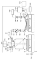
図1は、スリット・スキャン方式の投影露光装置の部分概略図である。レチクル2はレチクルステージ3上に保持され、レチクル(原版)2のパターンは縮小投影レンズ系1の倍率で1/4ないし1/2、或いは1/5に縮小投影されその像面に像を形成する。
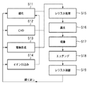
次に、図15及び図16を参照して、上述の露光装置を利用したデバイス製造方法の実施例を説明する。図15は、デバイス(ICやLSIなどの半導体チップ、LCD、CCD等)の製造を説明するためのフローチャートである。ここでは、半導体チップの製造方法を例に説明する。
2・・・レチクル
3・・・レチクルステージ
4・・・基板
5・・・基板チャック
6・・・露光ステージ
7・・・定盤
8・・・照明光学系
9・・・基準面
10・・・光源
11・・・コリメータレンズ
12・・・プリズム形状のスリット部材
13,16・・・計測レンズ
14,15・・・折り曲げミラー
17・・・ストッパー絞り
18・・・補正光学系群
19・・・光電変換器群
20・・・レチクルXYバーミラー
21・・・レチクルステージ干渉計
22・・・計測ステージ
23・・・合焦用マーク
24・・・ハーフミラー
25・・・集光レンズ
26・・・計測器
27・・・ステージバーミラー
28・・・ステージ干渉計
100・・・高さ計測器
110・・・メイン制御部
111・・・制御器
120・・・ドライバ
130・・・メモリ
140・・・コンソール
300、301、302、303・・・基板周辺の非四辺形ショット領域
304、305・・・四辺形ショット領域
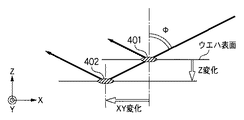
401、402・・・計測箇所
601、602、603、604、605、606・・・チップ
1201・・・境界線
1202・・・有効無効自動判定エリアの左右幅
1203・・・有効無効自動判定エリアの上下幅
1204・・・無効領域
1205・・・有効領域
1301、1302・・・境界線
Claims (3)
- 原版からの光を基板に投影する投影光学系を有し、該原版及び前記投影光学系を介して該基板の各ショット領域を露光する露光装置であって、
該基板を保持し、かつ移動する基板ステージと、
前記各ショット領域の内側の一部の領域のみに有効領域を設定するコンソールと、
該基板の表面における複数の計測箇所において前記投影光学系の光軸の方向における該表面の位置を計測する計測器と、
該複数の計測箇所のうち前記コンソールによって設定された該有効領域内に位置する計測箇所に関して前記計測器により計測された該表面の位置に基づいて、前記基板ステージの該光軸の方向における位置を制御する制御器と、
を備えることを特徴とする露光装置。 - 前記制御器は、該複数の計測箇所のうち少なくとも一つの計測箇所に関して、前記計測器によって計測された該表面の位置に基づいて該表面における計測箇所の位置を求め、求められた該表面における計測箇所の位置に基づいて該有効領域内に位置する計測箇所を特定することを特徴とする請求項1に記載の露光装置。
- 請求項1又は請求項2に記載される露光装置を用いて基板を露光する工程と、
前記工程で該露光された基板を現像する工程とを備えることを特徴とするデバイス製造方法。
Priority Applications (2)
| Application Number | Priority Date | Filing Date | Title |
|---|---|---|---|
| JP2006322518A JP5692949B2 (ja) | 2006-11-29 | 2006-11-29 | 露光装置 |
| US11/945,623 US7852458B2 (en) | 2006-11-29 | 2007-11-27 | Exposure apparatus |
Applications Claiming Priority (1)
| Application Number | Priority Date | Filing Date | Title |
|---|---|---|---|
| JP2006322518A JP5692949B2 (ja) | 2006-11-29 | 2006-11-29 | 露光装置 |
Publications (3)
| Publication Number | Publication Date |
|---|---|
| JP2008140794A JP2008140794A (ja) | 2008-06-19 |
| JP2008140794A5 JP2008140794A5 (ja) | 2010-02-12 |
| JP5692949B2 true JP5692949B2 (ja) | 2015-04-01 |
Family
ID=39463336
Family Applications (1)
| Application Number | Title | Priority Date | Filing Date |
|---|---|---|---|
| JP2006322518A Active JP5692949B2 (ja) | 2006-11-29 | 2006-11-29 | 露光装置 |
Country Status (2)
| Country | Link |
|---|---|
| US (1) | US7852458B2 (ja) |
| JP (1) | JP5692949B2 (ja) |
Families Citing this family (5)
| Publication number | Priority date | Publication date | Assignee | Title |
|---|---|---|---|---|
| NL1036557A1 (nl) * | 2008-03-11 | 2009-09-14 | Asml Netherlands Bv | Method and lithographic apparatus for measuring and acquiring height data relating to a substrate surface. |
| US8120304B2 (en) * | 2008-12-12 | 2012-02-21 | Formfactor, Inc. | Method for improving motion times of a stage |
| US11885738B1 (en) | 2013-01-22 | 2024-01-30 | J.A. Woollam Co., Inc. | Reflectometer, spectrophotometer, ellipsometer or polarimeter system including sample imaging system that simultaneously meet the scheimpflug condition and overcomes keystone error |
| JP5734344B2 (ja) * | 2013-05-16 | 2015-06-17 | キヤノン株式会社 | 露光装置および物品の製造方法 |
| NL2017846A (en) * | 2015-12-21 | 2017-06-27 | Asml Netherlands Bv | Height Measurement Apparatus |
Family Cites Families (13)
| Publication number | Priority date | Publication date | Assignee | Title |
|---|---|---|---|---|
| US6304317B1 (en) * | 1993-07-15 | 2001-10-16 | Nikon Corporation | Projection apparatus and method |
| JP3919689B2 (ja) * | 1994-06-14 | 2007-05-30 | キヤノン株式会社 | 露光方法、素子の製造方法および露光装置 |
| JPH10116877A (ja) * | 1996-10-14 | 1998-05-06 | Canon Inc | 面位置検出装置および方法、それを用いた露光方式、ならびにデバイス製造方法 |
| US6538723B2 (en) * | 1996-08-05 | 2003-03-25 | Nikon Corporation | Scanning exposure in which an object and pulsed light are moved relatively, exposing a substrate by projecting a pattern on a mask onto the substrate with pulsed light from a light source, light sources therefor, and methods of manufacturing |
| JPH1092722A (ja) * | 1996-09-18 | 1998-04-10 | Nikon Corp | 露光装置 |
| JP2001250768A (ja) * | 2000-03-08 | 2001-09-14 | Nikon Corp | 露光装置 |
| JP2003203855A (ja) * | 2002-01-10 | 2003-07-18 | Nikon Corp | 露光方法及び露光装置、並びにデバイス製造方法 |
| JP3899958B2 (ja) * | 2002-02-28 | 2007-03-28 | ソニー株式会社 | 露光装置および露光方法 |
| JP2004071851A (ja) * | 2002-08-07 | 2004-03-04 | Canon Inc | 半導体露光方法及び露光装置 |
| JP4652667B2 (ja) * | 2003-02-13 | 2011-03-16 | キヤノン株式会社 | 面位置計測方法及び走査型露光装置 |
| JP3870182B2 (ja) * | 2003-09-09 | 2007-01-17 | キヤノン株式会社 | 露光装置及びデバイス製造方法 |
| JP2006108474A (ja) * | 2004-10-07 | 2006-04-20 | Canon Inc | 露光装置及びそれを用いたデバイス製造方法 |
| JP2006275555A (ja) * | 2005-03-28 | 2006-10-12 | Canon Inc | 表面形状測定方法、表面形状測定装置、露光方法、及び露光装置 |
-
2006
- 2006-11-29 JP JP2006322518A patent/JP5692949B2/ja active Active
-
2007
- 2007-11-27 US US11/945,623 patent/US7852458B2/en active Active
Also Published As
| Publication number | Publication date |
|---|---|
| US7852458B2 (en) | 2010-12-14 |
| JP2008140794A (ja) | 2008-06-19 |
| US20080123075A1 (en) | 2008-05-29 |
Similar Documents
| Publication | Publication Date | Title |
|---|---|---|
| KR100875008B1 (ko) | 노광장치 및 디바이스 제조방법 | |
| JP3376179B2 (ja) | 面位置検出方法 | |
| KR101444981B1 (ko) | 노광 장치, 노광 방법 및 디바이스 제조 방법 | |
| JPH07270122A (ja) | 変位検出装置、該変位検出装置を備えた露光装置およびデバイスの製造方法 | |
| KR100517159B1 (ko) | 노광장치 및 방법 | |
| JP2009038359A (ja) | 露光装置およびデバイス製造方法 | |
| JP3880155B2 (ja) | 位置決め方法及び位置決め装置 | |
| JP5692949B2 (ja) | 露光装置 | |
| JP4280523B2 (ja) | 露光装置及び方法、デバイス製造方法 | |
| JP5137879B2 (ja) | 露光装置及びデバイス製造方法 | |
| JP3335126B2 (ja) | 面位置検出装置及びそれを用いた走査型投影露光装置 | |
| JPH1092731A (ja) | 投影露光装置 | |
| US20090310108A1 (en) | Exposure apparatus and method of manufacturing device | |
| JP4174324B2 (ja) | 露光方法及び装置 | |
| JP2010258085A (ja) | 面位置検出方法 | |
| JP3428825B2 (ja) | 面位置検出方法および面位置検出装置 | |
| JP2013247304A (ja) | 基板保持装置、露光装置、およびデバイス製造方法 | |
| JP2010114265A (ja) | 走査露光装置およびその制御方法、ならびにデバイス製造方法 | |
| JP2009194247A (ja) | 露光装置 | |
| JP2005175383A (ja) | 露光装置、アライメント方法、及び、デバイスの製造方法 | |
| JPH1064980A (ja) | 面位置検出装置および方法 | |
| JP2005209926A (ja) | マーク検出方法とその装置、露光方法とその装置、及び、デバイス製造方法 | |
| JP2008118061A (ja) | 露光装置 | |
| JP3531895B2 (ja) | 投影露光装置 | |
| JP2022160187A (ja) | 露光装置、露光方法及び物品の製造方法 |
Legal Events
| Date | Code | Title | Description |
|---|---|---|---|
| A621 | Written request for application examination |
Free format text: JAPANESE INTERMEDIATE CODE: A621 Effective date: 20091130 |
|
| A521 | Request for written amendment filed |
Free format text: JAPANESE INTERMEDIATE CODE: A523 Effective date: 20091217 |
|
| A977 | Report on retrieval |
Free format text: JAPANESE INTERMEDIATE CODE: A971007 Effective date: 20111027 |
|
| A131 | Notification of reasons for refusal |
Free format text: JAPANESE INTERMEDIATE CODE: A131 Effective date: 20111031 |
|
| A521 | Request for written amendment filed |
Free format text: JAPANESE INTERMEDIATE CODE: A523 Effective date: 20111222 |
|
| A131 | Notification of reasons for refusal |
Free format text: JAPANESE INTERMEDIATE CODE: A131 Effective date: 20120924 |
|
| A521 | Request for written amendment filed |
Free format text: JAPANESE INTERMEDIATE CODE: A523 Effective date: 20121122 |
|
| A02 | Decision of refusal |
Free format text: JAPANESE INTERMEDIATE CODE: A02 Effective date: 20130816 |
|
| A521 | Request for written amendment filed |
Free format text: JAPANESE INTERMEDIATE CODE: A523 Effective date: 20131115 |
|
| A911 | Transfer to examiner for re-examination before appeal (zenchi) |
Free format text: JAPANESE INTERMEDIATE CODE: A911 Effective date: 20131125 |
|
| A912 | Re-examination (zenchi) completed and case transferred to appeal board |
Free format text: JAPANESE INTERMEDIATE CODE: A912 Effective date: 20131220 |
|
| A521 | Request for written amendment filed |
Free format text: JAPANESE INTERMEDIATE CODE: A523 Effective date: 20141128 |
|
| A61 | First payment of annual fees (during grant procedure) |
Free format text: JAPANESE INTERMEDIATE CODE: A61 Effective date: 20150203 |
|
| R151 | Written notification of patent or utility model registration |
Ref document number: 5692949 Country of ref document: JP Free format text: JAPANESE INTERMEDIATE CODE: R151 |