JP5692949B2 - Exposure equipment - Google Patents
Exposure equipment Download PDFInfo
- Publication number
- JP5692949B2 JP5692949B2 JP2006322518A JP2006322518A JP5692949B2 JP 5692949 B2 JP5692949 B2 JP 5692949B2 JP 2006322518 A JP2006322518 A JP 2006322518A JP 2006322518 A JP2006322518 A JP 2006322518A JP 5692949 B2 JP5692949 B2 JP 5692949B2
- Authority
- JP
- Japan
- Prior art keywords
- substrate
- measurement
- exposure
- area
- stage
- Prior art date
- Legal status (The legal status is an assumption and is not a legal conclusion. Google has not performed a legal analysis and makes no representation as to the accuracy of the status listed.)
- Active
Links
Images


Classifications
-
- G—PHYSICS
- G03—PHOTOGRAPHY; CINEMATOGRAPHY; ANALOGOUS TECHNIQUES USING WAVES OTHER THAN OPTICAL WAVES; ELECTROGRAPHY; HOLOGRAPHY
- G03F—PHOTOMECHANICAL PRODUCTION OF TEXTURED OR PATTERNED SURFACES, e.g. FOR PRINTING, FOR PROCESSING OF SEMICONDUCTOR DEVICES; MATERIALS THEREFOR; ORIGINALS THEREFOR; APPARATUS SPECIALLY ADAPTED THEREFOR
- G03F9/00—Registration or positioning of originals, masks, frames, photographic sheets or textured or patterned surfaces, e.g. automatically
- G03F9/70—Registration or positioning of originals, masks, frames, photographic sheets or textured or patterned surfaces, e.g. automatically for microlithography
- G03F9/7003—Alignment type or strategy, e.g. leveling, global alignment
- G03F9/7023—Aligning or positioning in direction perpendicular to substrate surface
- G03F9/7026—Focusing
Description
本発明は、半導体デバイス等のデバイスの製造に使用する露光装置に関する The present invention relates to an exposure apparatus used for manufacturing a device such as a semiconductor device.
例えば半導体素子、液晶表示素子、薄膜磁気ヘッド等をリソグラフィ工程で製造する際に、マスク又はレチクル(以下、「レチクル」と総称する。)のパターン及び投影光学系を介して基板を露光する露光装置が使用される。 For example, when a semiconductor element, a liquid crystal display element, a thin film magnetic head or the like is manufactured in a lithography process, an exposure apparatus that exposes a substrate via a mask or reticle (hereinafter, collectively referred to as “reticle”) pattern and a projection optical system. Is used.
露光装置においては、集積回路の微細化、高密度化に伴いレチクル面上の回路パターンを基板面上に高い解像力で投影露光することが要求される。回路パターンの投影解像力は、投影光学系の開口数(NA)と露光波長に依存する。そこで、投影光学系のNAを大きくしたり、例えばg線よりi線、i線よりエキシマレーザー発振波長、エキシマレーザー発振波長でも、248nm、193nm、更には157nmというように短波長化の取り組みが行われている。 An exposure apparatus is required to project and expose a circuit pattern on a reticle surface onto a substrate surface with high resolution as the integrated circuit is miniaturized and densified. The projection resolution of the circuit pattern depends on the numerical aperture (NA) of the projection optical system and the exposure wavelength. Therefore, efforts have been made to increase the NA of the projection optical system, or to shorten the wavelength such as 248 nm, 193 nm, and even 157 nm even for the excimer laser oscillation wavelength and the excimer laser oscillation wavelength from the g-line, i-line, and i-line. It has been broken.
露光面積の大画面化も進んでいる。これらを達成する手段として、ほぼ正方形状に近い露光領域を基板上に縮小して一括投影露光する方式のステッパーや、露光領域を矩形又は円弧のスリット形状とし、レチクルと基板を相対的に高速走査して大画面を精度良く露光するスキャナーがある。スキャナーは、走査露光スリット単位で基板の表面形状を最適露光像面位置に合わせ込むため、基板平面度の影響も低減できる効果を有する。スキャナーは、ステッパーと同等のレンズを使いながら、露光領域とNAを大きくすることができる。そのため、スキャナーは露光装置の主流となってきている。 The screen size of the exposure area is also increasing. As a means to achieve these, a stepper that reduces the exposure area close to a square shape onto the substrate and performs batch projection exposure, or makes the exposure area a rectangular or arc slit shape, and relatively fast scans between the reticle and the substrate There is a scanner that accurately exposes a large screen. Since the scanner adjusts the surface shape of the substrate to the optimum exposure image plane position in units of scanning exposure slits, it has an effect of reducing the influence of the substrate flatness. The scanner can increase the exposure area and NA while using a lens equivalent to a stepper. Therefore, scanners have become the mainstream of exposure apparatuses.
走査型露光装置、通称スキャナーは、走査露光スリット内で基板表面を露光像面位置にリアルタイムで合わせ込む。そのために、露光スリットに差し掛かる前に基板表面位置を光斜入射系の表面位置計測器や、エアーマイクロセンサ、静電容量センサ等のギャップセンサを用いて計測し、基板を移動させる。特に、露光スリットの長手方向(走査方向と直交する方向)には、高さのみならず表面の傾きを計測すべく複数の計測箇所を有している。 A scanning exposure apparatus, commonly called a scanner, aligns the substrate surface with the exposure image plane position in real time within the scanning exposure slit. Therefore, before reaching the exposure slit, the substrate surface position is measured using a gap position sensor such as a light oblique incidence system surface position measuring instrument, an air micro sensor, or a capacitance sensor, and the substrate is moved. In particular, in the longitudinal direction of the exposure slit (direction orthogonal to the scanning direction), there are a plurality of measurement points for measuring not only the height but also the surface inclination.
図9では、走査露光スリットの前後に表面位置計測器の計測箇所をそれぞれ三点ずつ有している。図10では、計測箇所を五点ずつ有している。前後に計測箇所を有することで、露光の為の走査が正負いずれの方向であっても、露光する前に基板のフォーカス計測が可能になっている。 In FIG. 9, there are three measurement points of the surface position measuring instrument before and after the scanning exposure slit. In FIG. 10, there are five measurement points. By having measurement positions before and after, it is possible to measure the focus of the substrate before exposure regardless of whether the scanning for exposure is positive or negative.
縮小される焦点深度に対し高いフォーカス補正精度を達成し、一枚の基板あたりの歩留まり向上を達成する方法が提案されている。その方法では、露光装置とは別に構成したフォーカス計測系により、基板の面位置を事前に求め、該面位置を使用してフォーカス、チルトを制御・駆動する。 There has been proposed a method of achieving high focus correction accuracy with respect to the reduced depth of focus and improving the yield per substrate. In this method, a surface position of the substrate is obtained in advance by a focus measurement system configured separately from the exposure apparatus, and focus and tilt are controlled and driven using the surface position.
四辺形の露光領域を逐次円形の基板上に転写していく場合、図5に示すように、基板の周辺部では露光領域の一部が基板領域からはみ出しうる。図6に示すように、露光領域内を複数のチップで構成するいわゆるマルチチップ構成でも、基板周辺領域で一部のチップが基板領域からはみ出しうる。そのため、一部が欠如している露光領域501(非四辺形部分)も通常通り露光する必要がある。 When the quadrilateral exposure area is sequentially transferred onto a circular substrate, as shown in FIG. 5, a part of the exposure area can protrude from the substrate area at the periphery of the substrate. As shown in FIG. 6, even in a so-called multi-chip configuration in which the exposure area is composed of a plurality of chips, some chips can protrude from the substrate area in the peripheral area of the substrate. Therefore, it is necessary to expose the exposure region 501 (non-quadogram portion) that is partially missing as usual.
また、CPUなどのように露光領域内1チップ構成の場合、イオン注入やRIE工程等で基板表面をクランピングする際に基板周辺に残存しているフォトレジストが剥離する。剥離したフォトレジストは、チップ領域のパターン部に移動し、パターン欠陥や寸法欠陥を引き起こすことがある。この場合チップの歩留まりが悪化するので、非四辺形部分にも、余分なレジストを除去する目的で、露光を行っている。 In the case of a one-chip configuration in the exposure region such as a CPU, the photoresist remaining around the substrate is peeled off when the substrate surface is clamped by ion implantation or RIE process. The peeled photoresist moves to the pattern part of the chip region and may cause a pattern defect or a dimensional defect. In this case, since the yield of the chip is deteriorated, the non-quadogram portion is exposed for the purpose of removing excess resist.
基板やチップ等のレイアウト情報から事前に走査計測時の基板表面位置の計測箇所の有効/無効判定を行い、走査露光中のフォーカス計測センサ(計測箇所)をダイナミックに切り換えながらフォーカスを計測、補正する方法がある。この方法は、基板周辺領域で露光領域の一部が欠如している非四辺形部分において、高精度な面位置計測と良好な露光とを実現している。この方法は、特許文献1に示されている。
しかしながら、近年のネットワーク社会の広がりと共にLSIに対する高性能化(高集積化、チップサイズの縮小、高速化、低消費電力化等)の要求は厳しさを増している。こうした要求に対して、半導体国際ロードマップ(ITRS)にのっとり、世代毎に配線の更なる微細化と多層化の実現を推し進めた結果、新たな問題も現出している。それは、微細化トレンドにしたがって焦点深度がきわめて小さくなり、露光すべき基板表面を最良結像面に合わせ込む精度の問題である。特に表面形状精度(平坦度)が悪い基板において、露光領域のフォーカス計測精度が問題となる。 However, with the spread of the network society in recent years, the demand for higher performance (high integration, chip size reduction, high speed, low power consumption, etc.) for the LSI has become severe. In response to these demands, new problems have emerged as a result of further miniaturization and multilayering of wiring for each generation in accordance with the International Semiconductor Roadmap (ITRS). That is, the depth of focus becomes extremely small in accordance with the miniaturization trend, and it is a problem of the accuracy of aligning the substrate surface to be exposed with the best imaging plane. In particular, in a substrate having poor surface shape accuracy (flatness), focus measurement accuracy in the exposure area becomes a problem.
露光装置の焦点深度に対して基板の平坦度の制御要求は、一般的に焦点深度の1/10〜1/5であり、焦点深度が0.4μmの場合、0.04μm〜0.08μmのオーダーで面内バラツキが生じる。図11に示すように、所定の間隔で配置された計測箇所FP1〜3の情報を基に基板の駆動を行うとする。計測箇所間で基板面位置情報が欠落しているから、FP1、FP2、FP3から求まる平面とのズレ量Δだけデフォーカスが発生し得る。この問題は、いわゆるフォーカスサンプリング誤差の問題でもある。 The request for controlling the flatness of the substrate with respect to the depth of focus of the exposure apparatus is generally 1/10 to 1/5 of the depth of focus, and when the depth of focus is 0.4 μm, it is 0.04 μm to 0.08 μm. In-plane variation occurs in order. As shown in FIG. 11, it is assumed that the substrate is driven based on the information of the measurement points FP1 to FP3 arranged at predetermined intervals. Since the substrate surface position information is missing between the measurement points, defocusing can occur by a deviation amount Δ from the plane obtained from FP1, FP2, and FP3. This problem is also a so-called focus sampling error problem.
この問題を解決するために、フォーカスサンプリング間隔を極力細かくすると共に、計測箇所の位置を厳密に管理した多点フォーカス計測系を構築し、フォーカス精度ばらつきの影響を低減することが考えられる。しかしながら、フォーカス計測箇所の数の増加に比例して、メカ公差/調整公差が増大し、製造難易度が高くなって、広義のコストが増加する。また、基板上の多点フォーカス計測位置がメカ公差/調整公差を持つことは、そのまま装置毎の機差となる。例えば銅配線に代表されるような反射率差の大きい下地パターンにおいては、計測位置の微小な違いがフォーカス補正精度のばらつき要因となる。 In order to solve this problem, it is conceivable to reduce the influence of variations in focus accuracy by reducing the focus sampling interval as much as possible and constructing a multi-point focus measurement system that strictly manages the position of the measurement location. However, in proportion to the increase in the number of focus measurement points, the mechanical tolerance / adjustment tolerance increases, the manufacturing difficulty increases, and the cost in a broad sense increases. In addition, the fact that the multipoint focus measurement position on the substrate has a mechanical tolerance / adjustment tolerance is a machine difference for each apparatus. For example, in a base pattern having a large reflectance difference as represented by copper wiring, a minute difference in the measurement position causes a variation in focus correction accuracy.
本発明は、例えば、基板表面を像面に高精度に位置合わせをすることができる露光装置を提供することを目的とする。
An object of the present invention is to provide, for example , an exposure apparatus that can align a substrate surface with an image plane with high accuracy.
本発明は、原版からの光を基板に投影する投影光学系を有し、原版及び投影光学系を介して基板の各ショット領域を露光する露光装置であって、基板を保持し、かつ移動する基板ステージと、各ショット領域の内側の一部の領域のみに有効領域を設定するコンソールと、基板の表面における複数の計測箇所において投影光学系の光軸の方向における表面の位置を計測する計測器と、複数の計測箇所のうちコンソールによって設定された有効領域内に位置する計測箇所に関して計測器により計測された表面の位置に基づいて、基板ステージの光軸の方向における位置を制御する制御器と、を備えることを特徴とする。 The present invention is an exposure apparatus that has a projection optical system that projects light from an original onto a substrate, and that exposes each shot area of the substrate via the original and the projection optical system, and holds and moves the substrate A substrate stage, a console that sets an effective area only in a part of the area inside each shot area, and a measuring instrument that measures the position of the surface in the direction of the optical axis of the projection optical system at multiple measurement locations on the surface of the substrate And a controller for controlling the position of the substrate stage in the direction of the optical axis based on the position of the surface measured by the measuring instrument with respect to the measuring position located within the effective region set by the console among the plurality of measuring positions; It is characterized by providing.
本発明の実施形態によれば、制御器は、複数の計測箇所のうち少なくとも一つの計測箇所に関して、計測器によって計測された表面の位置に基づいて表面における計測箇所の位置を求め、求められた表面における計測箇所の位置に基づいて有効領域内に位置する計測箇所を特定することが好ましい。 According to the embodiment of the present invention, the controller obtains the position of the measurement location on the surface based on the position of the surface measured by the measurement device with respect to at least one measurement location among the plurality of measurement locations . It is preferable to specify the measurement location located in the effective region based on the position of the measurement location on the surface .
本発明によれば、例えば、基板表面を像面に高精度に位置合わせをすることができる露光装置を提供することができる。 According to the present invention, for example , it is possible to provide an exposure apparatus capable of aligning the substrate surface with the image plane with high accuracy.
図面を参照しながら本発明に係る一実施形態を説明する。 An embodiment according to the present invention will be described with reference to the drawings.
[露光装置の実施形態]
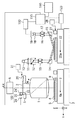
図1は、スリット・スキャン方式の投影露光装置の部分概略図である。レチクル2はレチクルステージ3上に保持され、レチクル(原版)2のパターンは縮小投影レンズ系1の倍率で1/4ないし1/2、或いは1/5に縮小投影されその像面に像を形成する。
[Embodiment of exposure apparatus]
FIG. 1 is a partial schematic view of a slit scanning type projection exposure apparatus. The
表面にレジストが塗布された基板4には、先の露光工程で形成された同一のパターン構造を有する多数個の被露光領域(ショット領域)が配列されている。基板4は保持治具である基板チャック5に吸着・固定される。基板チャック5は基板ステージ6に固定されている。基板ステージ6は、XYステージ、Z軸方向の移動やX、Y軸回りに回転可能なレベリングステージ、Z軸回りに回転可能な回転ステージにより構成されうる。レチクルパターン像を基板上の被露光領域に合致させるための6軸補正系を構成する基板ステージ6(以下、「露光ステージ」という。)は定盤7上に設置される。
A large number of exposed areas (shot areas) having the same pattern structure formed in the previous exposure process are arranged on the
第一の高さ位置計測器10〜19は、基板4の表面位置及び傾きを計測するために設けた計測光学系の各要素である。光源10は、白色ランプ又は相異なる複数のピーク波長を持つ高輝度発光ダイオードの光を照射する照明ユニットよりなる。コリメータレンズ11は、光源10からの光束を断面の強度分布がほほ均一の平行光束として射出する。プリズム形状のスリット部材12は、一対のプリズムを互いの斜面が相対する様に貼り合わせ、この貼り合わせ面に複数の開口(例えば25個のピンホール)をクロム等の遮光膜を利用して設けている。両テレセントリック系の光学系13は、スリット部材12の複数のピンホールを通過した独立の25本の光束をミラー14を介して基板4面上の25個の計測スポットに導光する。図1では1光束しか示されていないが、各光束は紙面垂直方向に25本の光束を有している。光学系13に対してピンホールの形成されている平面と基板4の表面を含む平面とはシャインプルーフの条件を満足するように設定している。
The first height
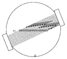
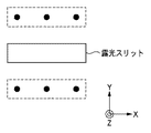
本実施形態において光照射手段からの各光束の基板4面上への入射角Φ(基板面にたてた垂線即ち光軸となす角) は70°以上である。基板4面上には、図3に示すように、同一パターン構造を有する複数個のショット領域が配列されている。光学系13を通過した25本の光束は、図2に示すように、パターン領域の互いに独立した各計測スポットに入射・結像している。図2における25個の計測スポットはX方向に、露光ステージにおける露光スリットの非スキャン方向の幅とほぼ等しいか、又はそれ以上の長さにわたって配置している。25個の計測スポットを、例えば露光ステージにおける露光スリット幅の倍の領域に亙って配置することで、少なくとも2つのショット領域を同時に計測することができ、全ショット領域を計測する時間が短縮される。25個の計測スポットが基板4面内で互いに独立して観察されるように、X方向(スキャン方向6a)からXY平面内でθ°(例えば22.5°) 回転させた方向より入射させる。
In this embodiment, the incident angle Φ (perpendicular to the substrate surface, that is, the angle formed with the optical axis) of each light beam from the light irradiation means on the surface of the
両テレセントリック系の受光光学系16は、ミラー15を介して基板4面からの25本の反射光束を受光する。受光光学系16内に設けたストッパー絞り17は25個の各計測スポットに対して共通に設けられ、基板4上に存在する回路パターンによって発生する高次の回折光 (ノイズ光) をカットする。両テレセントリック系の受光光学系16を通過した光束は、補正光学系群18の25個の個別の補正レンズにより光電変換器群19の計測面に、互いに同一の大きさのスポット光となるように再結像する。受光する側の要素16〜18は、基板4面上の各計測スポットと光電変換器群19の計測面とが、互いに共役となるように倒れ補正を行っている。そのため、各計測スポットの局所的な傾きにより計測面でのピンホール像の位置が変化することはなく、各計測スポットの光軸方向AXでの高さ変化に応答して計測面上でピンホール像が変化する。この実施形態では光電変換器群19は25個の例えば一次元CCDラインセンサであるが、複数の二次元位置計測素子でもよい。
Both telecentric light receiving
レチクルステージ3に吸着・固定されたレチクル2は、図1に示す矢印3a(Y軸方向)方向に一定速度でスキャンするとともに矢印3aと直交する方向 (X軸方向)には目標座標位置を維持してスキャンする様に補正駆動される。レチクルステージのX、Y方向の位置情報は、レチクルステージ3に固定されたXYバーミラー20へ外部のレチクル干渉系21から複数のレーザービームが照射されることにより常時計測される。
The
照明光学系8は、エキシマレーザー等のパルス光を発生する光源、ビーム整形光学系、オプティカルインテグレイダー、コリメータ及びミラー等の部材で構成されうる。照明光学系8は、遠紫外領域のパルス光を効率的に透過或いは反射する材料で形成されうる。ビーム整形光学系は、入射ビームの断面形状(寸法含む)を所望の形に整形する。オプティカル・インテグレータは光束の配光特性を均一にしてレチクル2を均一照度で照明する。
The illumination
照明光学系8内のマスキングブレードは、チップサイズに対応する矩形の照明領域を設定する。その照明領域で部分照明されたレチクル2上のパターンが投影レンズ1を介してレジストが塗布された基板4上に投影される。本実施形態の露光系は、照明光学系8及び縮小投影光学系1から定盤7に至る各要素より構成される。
The masking blade in the illumination
基板チャック5はその一部に基準面9が設けられる。定盤7上又は別に設けた定盤上には、露光ステージ6と同様に6軸方向に自由に移動可能な別の露光及び計測用の基板ステージ22(以下、「計測ステージ」という。)が配置される。基板チャック5及び基板4は、最初は計測ステージ22上にセットされる。
The
第一の高さ位置計測器は、計測ステージ22上にセットされた状態で基板チャック5上の基準面9に対する基板4上の各チップ又は任意のチップの高さ位置を計測し、計測データをメモリ130に記憶する。基板チャック5上の基準面9は、計測精度を高める為に基板4と略同一の高さとなるように、例えば金属薄膜や金属板等を付して構成されうる。
The first height position measuring device measures the height position of each chip or an arbitrary chip on the
本実施形態において、基板4は、真空吸着や静電気等の手段によって基板チャック5に吸着されたままで露光ステージ6上を移動する。基板4が所定面上に位置するように合焦操作を行う。第二の高さ位置計測器100は、基準面9を利用して高さ計測に相当する合焦操作を行う。例えばレチクル2上の露光可能領域(回路パターン)内又はその境界線上に設けた合焦用のマーク23と基準面9とを利用して合焦操作を行う。マーク23は例えばピンホールから成り、照明光学系8からの光が通過し、投影光学系1によって基板チャック5上の基準面9の近傍に結像する。基準面9で反射した光は再び投影光学系1でマーク23近傍に再結像する。レチクル2と基準面9が完全に合焦状態となったとき、マーク23を構成するピンホールを通過する光量は最大となる。計測器26は、Zステージを駆動させながらハーフミラー24と集光レンズ25を用いてこの最大光量を計測し、メイン制御部110へ入力する。メイン制御部110は、光量が最大になった位置で露光ステージ6が止まるように、ドライバ120を介してステージ位置(Z方向)を制御する。
In the present embodiment, the
ドライバ120は、露光ステージ6をX−Y面内で移動させて、コンソール140で設定される各種事前情報に従って基板面上の各チップを順次露光位置に移動させる。先に計測ステージ22上で計測し、メモリ130に記憶した基板5面上の基準面9に対する各チップの高さ位置がメイン制御部110に入力されている。ドライバ120は、その高さ位置に基づいて各チップが合焦位置にくるように露光ステージ6のZステージを駆動する。その後、露光を行う。
The
本実施形態の面位置計測方法及びその露光方法を図8のフローチャートを用いて説明する。 The surface position measuring method and the exposure method of this embodiment will be described with reference to the flowchart of FIG.
図1の装置において、光源10として例えば発光ダイオード(LED)を用い、受光器として例えば一次CCDセンサを用いる。
In the apparatus of FIG. 1, for example, a light emitting diode (LED) is used as the
ステップ801でメイン制御部110は制御を開始する。ステップ802でメイン制御部110は不図示の搬送ハンドに基板4を計測ステージ22上に搬入させ、チャック5に吸着固定させる。ステップ803でメイン制御部110は、基板サイズ・レイアウト情報からショット領域内計測間隔と、隣接ショット領域間の計測タイミング変化量を求めて計測位置情報とし、それを記憶する。基板サイズ・レイアウト情報は、例えば、コンソール140で設定される各種事前情報、スキャン計測領域の大きさ、ショット領域配置情報、走査スピード、CCD蓄積時間でありうる。
In step 801, the
ステップ804で、メイン制御部110は第一の高さ位置計測器10〜19等に、計測ステージ22において基板全域を例えば図3に示す順番にてスキャンと同期して計測させる。即ち、ショット領域300の手前でステージを加速して一定速度に達したあとは、等速スキャンでショット領域300内の計測箇所を連続的に計測し、次いでショット領域301、ショット領域302と連続的に計測する。ショット領域302の領域内での計測が完了したら速やかに減速しつつX方向に移動を開始して隣の列に移る。ショット領域303の手前でステージを加速して一定速度に達した後、等速スキャンでショット領域303、ショット領域304、ショット領域305と、Y方向の複数ショット領域を連続的に計測する。所定の範囲で計測が完了したら速やかに減速しつつX方向に移動して隣の列に移り、加速開始ポイントに達したらステージを反対方向に加速して等速スキャンでY方向の複数ショット領域を連続的に計測することを繰り返す。このようにすれば、ショット領域毎にステージを加速/減速する必要が無くなる為、短時間で基板全面の面位置計測が実現できる。メモリ130は基板全面の高さ位置を記憶する。
In step 804, the
ステップ805で、メイン制御部110の制御器111は有効計測箇所の判定と面位置の決定を行う。制御器111は、第1に第一の高さ位置計測器によって計測された計測箇所の表面の位置に基づいて基板の面方向位置を補正する。制御器111は、第2に後述する各ショット領域の有効領域の情報、又は、当該情報と補正された面方向位置とに基づいて有効領域に位置する計測箇所を特定する。制御器111は、第3に有効領域に位置すると判定された計測箇所の表面の位置に基づいて各ショット領域の面位置を決定する。制御器111は、上記3つの機能のうち少なくとも第2及び第3の機能を実行する。
In step 805, the controller 111 of the
まず、制御器111による有効計測箇所の判定方法を、図4〜図7、図12、図13を使って詳細に説明する。 First, the determination method of the effective measurement location by the controller 111 is demonstrated in detail using FIGS. 4-7, FIG. 12, FIG.
図5は3×2=6チップを1ショット領域とした場合の基板上のショット配列を示す。同図において網掛けショット領域は、一部が欠如したショット領域であり、図6に拡大した図を示している。図中、網掛けしたチップ603〜チップ606は、一部が欠如した無効チップであり、チップ601、チップ602が有効チップとなる。このように、基板の周辺部では露光領域の一部が基板領域からはみ出して露光される。
FIG. 5 shows a shot arrangement on the substrate when 3 × 2 = 6 chips are used as one shot area. In the figure, the shaded shot area is a shot area in which a part is missing, and an enlarged view is shown in FIG. In the drawing, shaded
図7(a)は有効チップに着目して面位置計測を行う様子を示している。図7(a)の○印及び●印は図5のショット配列におけるショット領域501での面位置計測箇所を表している。白抜き○印は有効な計測箇所位置を、塗り潰し●印が無効な計測箇所位置を夫々表している。
FIG. 7A shows a state in which the surface position is measured while paying attention to the effective chip. In FIG. 7A, the ◯ and ● marks represent the surface position measurement points in the
計測箇所位置は、例えば、計測箇所の配置間隔、スキャン計測領域の大きさ、ショット配置情報、走査スピード、CCD蓄積時間を基に、ショット領域内計測間隔、隣接ショット領域間の計測タイミング変化量から決定される。その後、コンソール140で設定されたショット領域毎の有効領域の情報に基づいて、計測箇所毎に有効/無効が判定される。上記ショット毎の有効領域の情報は、例えばコンソールを介して入力されうる。あるいは、ショット領域毎の有効領域の情報は通信回線を介して提供されることもできる。
The measurement location is determined from, for example, the measurement interval in the shot region, and the measurement timing change amount between adjacent shot regions based on the arrangement interval of the measurement location, the size of the scan measurement region, the shot arrangement information, the scanning speed, and the CCD accumulation time It is determined. Thereafter, the validity / invalidity of each measurement location is determined based on the information of the valid area for each shot area set on the
図12、図13(a)、(b)はショット領域内の計測箇所の有効/無効判定を行う計測値有効領域の例を図示したものである。いずれもショット領域をその外縁と境界線とによって有効領域と無効領域とに区切っている。使用する境界線の数は、縦及び横の少なくともいずれかの方向に1本以上であればよい。図13(a)では、縦横それぞれに1本の境界線を、図12、図13(b)では縦横それぞれに2本の境界線を使用している。図12では、縦横計4本の境界線により区分される9の領域のうち、ショット領域の外縁付近を除外するために、中央の白地領域1つのみが有効領域である。図13(a)では、縦横計2本の境界線により区分される4の領域のうち、右上の1つの白地領域が有効領域であり、図13(b)では、縦横計4本の境界線により区分される9の領域のうち、右上の6つの白地領域が有効領域である。本発明の実施形態では、このように境界線を用いて、計測箇所毎の有効/無効を簡易な方法によって設定している。 FIGS. 12, 13A, and 13B show examples of measurement value effective areas for performing validity / invalidity determination of measurement locations in a shot area. In both cases, the shot area is divided into an effective area and an ineffective area by an outer edge and a boundary line. The number of boundary lines to be used may be one or more in at least one of the vertical and horizontal directions. In FIG. 13A, one boundary line is used in each of the vertical and horizontal directions, and in FIG. 12 and FIG. 13B, two boundary lines are used in the vertical and horizontal directions. In FIG. 12, only one central white background area is an effective area in order to exclude the vicinity of the outer edge of the shot area among the nine areas divided by the four vertical and horizontal boundaries. In FIG. 13A, one white background area at the upper right is an effective area among four areas divided by two vertical and horizontal total boundary lines. In FIG. 13B, four vertical and horizontal total boundary lines are displayed. Among the nine areas divided by the above, the upper right six white background areas are effective areas. In the embodiment of the present invention, using the boundary line as described above, the validity / invalidity for each measurement point is set by a simple method.
計測箇所が無効領域内に位置する場合、制御器111はその計測箇所を面位置決定の基礎とはしない。制御器111は、有効領域内に位置する計測箇所の表面の位置計測結果に基づいて面位置を演算し、決定する。 When the measurement location is located in the invalid area, the controller 111 does not use the measurement location as a basis for determining the surface position. The controller 111 calculates and determines the surface position based on the position measurement result of the surface of the measurement location located in the effective area.
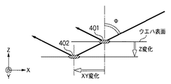
図7(b)は別の面位置計測装置における計測箇所配置の例である。計測箇所の面方向位置は、面位置計測装置のメカ公差、調整誤差等機差の影響や、図4のような斜入射光計測系の面位置計測装置においてZ変化により発生した計測箇所位置のXY変化の影響を受けている。図4は入射角ΦにおけるZ変化量に対するXY方向の変化量を説明した図である。計測された基板表面の位置401は基板表面のZ変化に伴って、Z×tanΦだけXY方向にシフトした点402に位置付けられることとなる。例えばΦ=70°ではtanΦ=2.747であるが、Φ=85°以上ではtanΦ=11.430以上となる。したがって、Z計測変化が大きい場合、当該Z計測値に対応するXYの計測値は、誤差の影響が大きく、そのまま使用することはできない。
FIG. 7B is an example of measurement location arrangement in another surface position measurement apparatus. The surface direction position of the measurement location is determined by the influence of mechanical tolerances, adjustment errors, etc. of the surface location measurement device, and the measurement location position caused by the Z change in the surface location measurement device of the oblique incident light measurement system as shown in FIG. Under the influence of XY changes. FIG. 4 is a diagram illustrating the amount of change in the XY direction with respect to the amount of Z change at the incident angle Φ. The measured
こうした機差の影響や、計測時の基板表面の高さ情報、基板を搭載したステージ姿勢に対応するために、境界線を用いて計測箇所の有効/無効の判定手法を変化させることができる。図12を用いて説明する。縦横2本の境界線1201とショット領域の外縁で包囲される領域1204は無効領域である。図中の1202と1203は左右上下の幅を意味しており、無効領域1204の範囲を定義している。制御器111は、高さ位置を示すZ計測結果に基づいて計測箇所の面方向位置を補正する。制御器111は、補正された面方向位置に基づいて計測箇所が有効か否かを判定する。制御器111は、有効領域内に位置すると判定した計測箇所の基板表面の位置に基づいてショット領域毎の面位置を演算し、決定する。
In order to cope with the influence of such machine differences, information on the height of the substrate surface at the time of measurement, and the posture of the stage on which the substrate is mounted, it is possible to change the determination method of validity / invalidity of the measurement location using the boundary line. This will be described with reference to FIG. A
以上のように、制御器111は、有効領域と無効領域とを区切る境界線、計測された基板表面の高さ位置の情報に基づいて、ショット領域内の計測箇所毎にその有効/無効を判断する。無効と判定された計測箇所の計測結果は面位置の演算に使用されない。制御器111は、有効と判定した計測箇所の計測結果のみに基づいて各ショット領域の面位置を演算し、決定する。 As described above, the controller 111 determines the validity / invalidity for each measurement location in the shot area based on the boundary line that divides the valid area and the invalid area and the information on the measured height position of the substrate surface. To do. The measurement result of the measurement location determined to be invalid is not used for the calculation of the surface position. The controller 111 calculates and determines the surface position of each shot area based only on the measurement result of the measurement location determined to be valid.
ステップ806で、制御器111は、ステップ805で決定したショット内の面位置の情報を記憶する。 In step 806, the controller 111 stores information on the surface position in the shot determined in step 805.
ステップ807で基板を基板チャックに吸着したまま露光ステージに移す。ステップ808でレチクル合焦用のマークと基板チャック上の基準面を使って合焦駆動させる。ステップ809で、基板チャック上の基準面に対する先に決定された面位置の情報に基づいて、ショット内の被露光領域を像面に合わせ込むべく基板ステージの位置を制御しながら、基板を露光する。 In step 807, the substrate is moved to the exposure stage while being adsorbed to the substrate chuck. In step 808, focusing is performed using the reticle focusing mark and the reference surface on the substrate chuck. In step 809, the substrate is exposed while controlling the position of the substrate stage so that the exposed area in the shot is aligned with the image plane based on the information of the surface position previously determined with respect to the reference surface on the substrate chuck. .
ステップ810でメイン制御部110は基板上の全ショットの露光が終了したかを判定する。露光が終了していなければ、ステップ809へ戻ってショット露光領域を像面へ補正しつつ交互スキャンしながらショット毎に露光を繰り返す。全ショットの露光が終了したらステップ811で基板を露光ステージから搬出して、ステップ812で一連の露光シーケンスを終了する。
In step 810, the
本実施形態は、図1に示したように、計測ステージと露光ステージとが別個に存在する露光装置とした。しかし、所謂オフラインでシステムが成立すれば、複数台の走査露光装置、又は一台の計測ステージと複数台の露光ステージで構成することも適用可能である。また、図14に示すようなシングルステージタイプの走査露光装置においても同様に適用することができる。 In the present embodiment, as shown in FIG. 1, an exposure apparatus in which a measurement stage and an exposure stage exist separately is used. However, if the system is established off-line, it is also possible to apply a plurality of scanning exposure apparatuses, or a single measurement stage and a plurality of exposure stages. Further, the present invention can be similarly applied to a single stage type scanning exposure apparatus as shown in FIG.
また、図8ではステップ801〜812まで一連の流れとして説明した。しかし、計測ステージと露光ステージが別個に存在することから明らかなように、ステップ807以降のスキャン露光と並行して次の基板を計測ステージに搬入して、ステップ801〜806の処理を行うことは充分に可能である。この場合、無駄なく連続的に基板を処理できる為、高効率な基板露光処理を実現できる。 Moreover, in FIG. 8, it demonstrated as a series of flow from step 801 to 812. FIG. However, as is clear from the fact that the measurement stage and the exposure stage exist separately, it is possible to carry the processing of steps 801 to 806 by carrying the next substrate into the measurement stage in parallel with the scan exposure after step 807. It is possible enough. In this case, since the substrate can be processed continuously without waste, highly efficient substrate exposure processing can be realized.
[デバイス製造の実施形態]
次に、図15及び図16を参照して、上述の露光装置を利用したデバイス製造方法の実施例を説明する。図15は、デバイス(ICやLSIなどの半導体チップ、LCD、CCD等)の製造を説明するためのフローチャートである。ここでは、半導体チップの製造方法を例に説明する。
[Device Manufacturing Embodiment]
Next, an embodiment of a device manufacturing method using the above-described exposure apparatus will be described with reference to FIGS. FIG. 15 is a flowchart for explaining how to fabricate devices (ie, semiconductor chips such as IC and LSI, LCDs, CCDs, and the like). Here, a semiconductor chip manufacturing method will be described as an example.
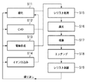
ステップS1(回路設計)では半導体デバイスの回路設計を行う。ステップS2(マスク製作)では設計した回路パターンに基づいてマスクを製作する。ステップS3(基板製造)ではシリコン等の材料を用いて基板を製造する。ステップS4(基板プロセス)は前工程と呼ばれ、マスクと基板を用いて、上記の露光装置によりリソグラフィ技術を利用して基板上に実際の回路を形成する。ステップS5(組み立て)は、後工程と呼ばれ、ステップS4によって作製された基板を用いて半導体チップ化する工程であり、アッセンブリ工程(ダイシング、ボンディング)、パッケージング工程(チップ封入)等の組み立て工程を含む。ステップS6(検査)では、ステップS5で作製された半導体デバイスの動作確認テスト、耐久性テスト等の検査を行う。こうした工程を経て半導体デバイスが完成し、それが出荷(ステップS7)される。 In step S1 (circuit design), a semiconductor device circuit is designed. In step S2 (mask production), a mask is produced based on the designed circuit pattern. In step S3 (substrate manufacture), a substrate is manufactured using a material such as silicon. Step S4 (substrate process) is called a pre-process, and an actual circuit is formed on the substrate using the mask and the substrate by the above exposure apparatus using the lithography technique. Step S5 (assembly) is called a post-process, and is a process for forming a semiconductor chip using the substrate manufactured in step S4. The assembly process includes an assembly process (dicing, bonding), a packaging process (chip encapsulation), and the like. including. In step S6 (inspection), inspections such as an operation check test and a durability test of the semiconductor device manufactured in step S5 are performed. Through these steps, the semiconductor device is completed and shipped (step S7).
図16は、ステップ4の基板プロセスの詳細なフローチャートである。ステップS11(酸化)では、基板の表面を酸化させる。ステップS12(CVD)では、基板の表面に絶縁膜を形成する。ステップS13(電極形成)では、基板上に電極を蒸着によって形成する。ステップS14(イオン打ち込み)では、基板にイオンを打ち込む。ステップS15(レジスト処理)では、基板に感光剤を塗布する。ステップS16(露光)では、露光装置によってマスクの回路パターンを基板に露光する。ステップS17(現像)では、露光した基板を現像する。ステップS18(エッチング)では、現像したレジスト像以外の部分を削り取る。ステップS19(レジスト剥離)では、エッチングが済んで不要となったレジストを取り除く。これらのステップを繰り返し行うことによって基板上に多重に回路パターンが形成される。
FIG. 16 is a detailed flowchart of the substrate process in
1・・・投影レンズ系
2・・・レチクル
3・・・レチクルステージ
4・・・基板
5・・・基板チャック
6・・・露光ステージ
7・・・定盤
8・・・照明光学系
9・・・基準面
10・・・光源
11・・・コリメータレンズ
12・・・プリズム形状のスリット部材
13,16・・・計測レンズ
14,15・・・折り曲げミラー
17・・・ストッパー絞り
18・・・補正光学系群
19・・・光電変換器群
20・・・レチクルXYバーミラー
21・・・レチクルステージ干渉計
22・・・計測ステージ
23・・・合焦用マーク
24・・・ハーフミラー
25・・・集光レンズ
26・・・計測器
27・・・ステージバーミラー
28・・・ステージ干渉計
100・・・高さ計測器
110・・・メイン制御部
111・・・制御器
120・・・ドライバ
130・・・メモリ
140・・・コンソール
300、301、302、303・・・基板周辺の非四辺形ショット領域
304、305・・・四辺形ショット領域
401、402・・・計測箇所
601、602、603、604、605、606・・・チップ
1201・・・境界線
1202・・・有効無効自動判定エリアの左右幅
1203・・・有効無効自動判定エリアの上下幅
1204・・・無効領域
1205・・・有効領域
1301、1302・・・境界線
DESCRIPTION OF
Claims (3)
該基板を保持し、かつ移動する基板ステージと、
前記各ショット領域の内側の一部の領域のみに有効領域を設定するコンソールと、
該基板の表面における複数の計測箇所において前記投影光学系の光軸の方向における該表面の位置を計測する計測器と、
該複数の計測箇所のうち前記コンソールによって設定された該有効領域内に位置する計測箇所に関して前記計測器により計測された該表面の位置に基づいて、前記基板ステージの該光軸の方向における位置を制御する制御器と、
を備えることを特徴とする露光装置。 An exposure apparatus having a projection optical system that projects light from an original onto a substrate, and exposing each shot region of the substrate through the original and the projection optical system,
A substrate stage for holding and moving the substrate;
A console for setting an effective area only in a part of the area inside each shot area;
A measuring instrument for measuring the position of the surface in the direction of the optical axis of the projection optical system at a plurality of measurement points on the surface of the substrate;
The position of the substrate stage in the direction of the optical axis is determined based on the position of the surface measured by the measuring instrument with respect to the measurement position located within the effective area set by the console among the plurality of measurement spots. A controller to control;
An exposure apparatus comprising:
前記工程で該露光された基板を現像する工程とを備えることを特徴とするデバイス製造方法。 A step of exposing the substrate using the exposure apparatus according to claim 1 or 2,
And a step of developing the substrate exposed in the step.
Priority Applications (2)
| Application Number | Priority Date | Filing Date | Title |
|---|---|---|---|
| JP2006322518A JP5692949B2 (en) | 2006-11-29 | 2006-11-29 | Exposure equipment |
| US11/945,623 US7852458B2 (en) | 2006-11-29 | 2007-11-27 | Exposure apparatus |
Applications Claiming Priority (1)
| Application Number | Priority Date | Filing Date | Title |
|---|---|---|---|
| JP2006322518A JP5692949B2 (en) | 2006-11-29 | 2006-11-29 | Exposure equipment |
Publications (3)
| Publication Number | Publication Date |
|---|---|
| JP2008140794A JP2008140794A (en) | 2008-06-19 |
| JP2008140794A5 JP2008140794A5 (en) | 2010-02-12 |
| JP5692949B2 true JP5692949B2 (en) | 2015-04-01 |
Family
ID=39463336
Family Applications (1)
| Application Number | Title | Priority Date | Filing Date |
|---|---|---|---|
| JP2006322518A Active JP5692949B2 (en) | 2006-11-29 | 2006-11-29 | Exposure equipment |
Country Status (2)
| Country | Link |
|---|---|
| US (1) | US7852458B2 (en) |
| JP (1) | JP5692949B2 (en) |
Families Citing this family (5)
| Publication number | Priority date | Publication date | Assignee | Title |
|---|---|---|---|---|
| NL1036557A1 (en) * | 2008-03-11 | 2009-09-14 | Asml Netherlands Bv | Method and lithographic apparatus for measuring and acquiring height data in relation to a substrate surface. |
| US8120304B2 (en) * | 2008-12-12 | 2012-02-21 | Formfactor, Inc. | Method for improving motion times of a stage |
| US11885738B1 (en) | 2013-01-22 | 2024-01-30 | J.A. Woollam Co., Inc. | Reflectometer, spectrophotometer, ellipsometer or polarimeter system including sample imaging system that simultaneously meet the scheimpflug condition and overcomes keystone error |
| JP5734344B2 (en) * | 2013-05-16 | 2015-06-17 | キヤノン株式会社 | Exposure apparatus and article manufacturing method |
| NL2017846A (en) * | 2015-12-21 | 2017-06-27 | Asml Netherlands Bv | Height Measurement Apparatus |
Family Cites Families (13)
| Publication number | Priority date | Publication date | Assignee | Title |
|---|---|---|---|---|
| US6304317B1 (en) * | 1993-07-15 | 2001-10-16 | Nikon Corporation | Projection apparatus and method |
| JP3919689B2 (en) * | 1994-06-14 | 2007-05-30 | キヤノン株式会社 | Exposure method, device manufacturing method, and exposure apparatus |
| JPH10116877A (en) * | 1996-10-14 | 1998-05-06 | Canon Inc | Device and method for detecting plane position, exposing method using it and production of device |
| US6538723B2 (en) * | 1996-08-05 | 2003-03-25 | Nikon Corporation | Scanning exposure in which an object and pulsed light are moved relatively, exposing a substrate by projecting a pattern on a mask onto the substrate with pulsed light from a light source, light sources therefor, and methods of manufacturing |
| JPH1092722A (en) * | 1996-09-18 | 1998-04-10 | Nikon Corp | Aligner |
| JP2001250768A (en) * | 2000-03-08 | 2001-09-14 | Nikon Corp | Projection aligner |
| JP2003203855A (en) * | 2002-01-10 | 2003-07-18 | Nikon Corp | Exposure method and aligner, and device manufacturing method |
| JP3899958B2 (en) * | 2002-02-28 | 2007-03-28 | ソニー株式会社 | Exposure apparatus and exposure method |
| JP2004071851A (en) * | 2002-08-07 | 2004-03-04 | Canon Inc | Semiconductor exposure method and aligner |
| JP4652667B2 (en) * | 2003-02-13 | 2011-03-16 | キヤノン株式会社 | Surface position measuring method and scanning exposure apparatus |
| JP3870182B2 (en) * | 2003-09-09 | 2007-01-17 | キヤノン株式会社 | Exposure apparatus and device manufacturing method |
| JP2006108474A (en) * | 2004-10-07 | 2006-04-20 | Canon Inc | Exposure device and display manufacturing method using the same |
| JP2006275555A (en) * | 2005-03-28 | 2006-10-12 | Canon Inc | Surface shape measuring method, surface shape measuring device, exposure method and exposure device |
-
2006
- 2006-11-29 JP JP2006322518A patent/JP5692949B2/en active Active
-
2007
- 2007-11-27 US US11/945,623 patent/US7852458B2/en active Active
Also Published As
| Publication number | Publication date |
|---|---|
| US20080123075A1 (en) | 2008-05-29 |
| US7852458B2 (en) | 2010-12-14 |
| JP2008140794A (en) | 2008-06-19 |
Similar Documents
| Publication | Publication Date | Title |
|---|---|---|
| KR100875008B1 (en) | Exposure apparatus and device manufacturing method | |
| JP3376179B2 (en) | Surface position detection method | |
| KR101444981B1 (en) | Exposure apparatus, exposure method, and method of manufacturing device | |
| JPH07270122A (en) | Displacement detection device, aligner provided with said displacement detection device and manufacture of device | |
| KR100517159B1 (en) | Exposure apparatus and method | |
| JP2009038359A (en) | Exposure apparatus and method for manufacturing device | |
| JP3880155B2 (en) | Positioning method and positioning device | |
| JP5692949B2 (en) | Exposure equipment | |
| JP4280523B2 (en) | Exposure apparatus and method, device manufacturing method | |
| JP5137879B2 (en) | Exposure apparatus and device manufacturing method | |
| JP3335126B2 (en) | Surface position detecting apparatus and scanning projection exposure apparatus using the same | |
| JPH1092731A (en) | Projection aligner | |
| US20090310108A1 (en) | Exposure apparatus and method of manufacturing device | |
| JP4174324B2 (en) | Exposure method and apparatus | |
| JP2010258085A (en) | Surface position detecting method | |
| JP3428825B2 (en) | Surface position detection method and surface position detection device | |
| JP2013247304A (en) | Substrate holding device, exposure device and device manufacturing method | |
| JP2010114265A (en) | Scanning exposure apparatus and control method therefor, and device manufacturing method | |
| JP2009194247A (en) | Exposure apparatus | |
| JP2005175383A (en) | Aligner, method of alignment and device manufacturing method | |
| JPH1064980A (en) | Device and method for detecting surface position | |
| JP2005209926A (en) | Mark detecting method and apparatus thereof, exposure method and apparatus thereof, and device manufacturing method | |
| JP2008118061A (en) | Exposure apparatus | |
| JP3531895B2 (en) | Projection exposure equipment | |
| JP2022160187A (en) | Exposure device, exposure method and manufacturing method of article |
Legal Events
| Date | Code | Title | Description |
|---|---|---|---|
| A621 | Written request for application examination |
Free format text: JAPANESE INTERMEDIATE CODE: A621 Effective date: 20091130 |
|
| A521 | Request for written amendment filed |
Free format text: JAPANESE INTERMEDIATE CODE: A523 Effective date: 20091217 |
|
| A977 | Report on retrieval |
Free format text: JAPANESE INTERMEDIATE CODE: A971007 Effective date: 20111027 |
|
| A131 | Notification of reasons for refusal |
Free format text: JAPANESE INTERMEDIATE CODE: A131 Effective date: 20111031 |
|
| A521 | Request for written amendment filed |
Free format text: JAPANESE INTERMEDIATE CODE: A523 Effective date: 20111222 |
|
| A131 | Notification of reasons for refusal |
Free format text: JAPANESE INTERMEDIATE CODE: A131 Effective date: 20120924 |
|
| A521 | Request for written amendment filed |
Free format text: JAPANESE INTERMEDIATE CODE: A523 Effective date: 20121122 |
|
| A02 | Decision of refusal |
Free format text: JAPANESE INTERMEDIATE CODE: A02 Effective date: 20130816 |
|
| A521 | Request for written amendment filed |
Free format text: JAPANESE INTERMEDIATE CODE: A523 Effective date: 20131115 |
|
| A911 | Transfer to examiner for re-examination before appeal (zenchi) |
Free format text: JAPANESE INTERMEDIATE CODE: A911 Effective date: 20131125 |
|
| A912 | Re-examination (zenchi) completed and case transferred to appeal board |
Free format text: JAPANESE INTERMEDIATE CODE: A912 Effective date: 20131220 |
|
| A521 | Request for written amendment filed |
Free format text: JAPANESE INTERMEDIATE CODE: A523 Effective date: 20141128 |
|
| A61 | First payment of annual fees (during grant procedure) |
Free format text: JAPANESE INTERMEDIATE CODE: A61 Effective date: 20150203 |
|
| R151 | Written notification of patent or utility model registration |
Ref document number: 5692949 Country of ref document: JP Free format text: JAPANESE INTERMEDIATE CODE: R151 |