JP5643230B2 - スピン注入トルク磁気抵抗ランダムアクセスメモリでのビットラインの電圧制御 - Google Patents
スピン注入トルク磁気抵抗ランダムアクセスメモリでのビットラインの電圧制御 Download PDFInfo
- Publication number
- JP5643230B2 JP5643230B2 JP2011548313A JP2011548313A JP5643230B2 JP 5643230 B2 JP5643230 B2 JP 5643230B2 JP 2011548313 A JP2011548313 A JP 2011548313A JP 2011548313 A JP2011548313 A JP 2011548313A JP 5643230 B2 JP5643230 B2 JP 5643230B2
- Authority
- JP
- Japan
- Prior art keywords
- bit line
- voltage
- stt
- mram
- read
- Prior art date
- Legal status (The legal status is an assumption and is not a legal conclusion. Google has not performed a legal analysis and makes no representation as to the accuracy of the status listed.)
- Expired - Fee Related
Links
Images


Classifications
-
- G—PHYSICS
- G11—INFORMATION STORAGE
- G11C—STATIC STORES
- G11C11/00—Digital stores characterised by the use of particular electric or magnetic storage elements; Storage elements therefor
- G11C11/02—Digital stores characterised by the use of particular electric or magnetic storage elements; Storage elements therefor using magnetic elements
- G11C11/16—Digital stores characterised by the use of particular electric or magnetic storage elements; Storage elements therefor using magnetic elements using elements in which the storage effect is based on magnetic spin effect
- G11C11/165—Auxiliary circuits
- G11C11/1673—Reading or sensing circuits or methods
-
- G—PHYSICS
- G11—INFORMATION STORAGE
- G11C—STATIC STORES
- G11C11/00—Digital stores characterised by the use of particular electric or magnetic storage elements; Storage elements therefor
- G11C11/02—Digital stores characterised by the use of particular electric or magnetic storage elements; Storage elements therefor using magnetic elements
- G11C11/16—Digital stores characterised by the use of particular electric or magnetic storage elements; Storage elements therefor using magnetic elements using elements in which the storage effect is based on magnetic spin effect
- G11C11/165—Auxiliary circuits
- G11C11/1659—Cell access
Description
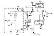
401 ビットセル
405 MTJ
410 ワードライントランジスタ、トランジスタ
420 ビットライン(BL)、ビットライン、BL
430 クランプ回路
440 ソースライン(SL)
450 読み出しアイソレーション素子、アイソレーション素子、素子
460 リファレンス
470 センスアンプ
480 書き込みドライバ
482、484 書き込みアイソレーション素子
502、504 プリチャージトランジスタ
600 時間
610 読み出しイネーブル信号rd_en
620 BL読み出しプリチャージ信号rdb、rdb
630 電圧
Claims (13)
- スピン注入トルク磁気抵抗ランダムアクセスメモリ(STT-MRAM)であって、
磁気トンネル接合(MTJ)およびワードライントランジスタを有するビットセルと、
ビットラインに接続されるクランプ回路と、
前記ビットラインの電圧とリファレンスビットラインの電圧との間の差に基づいて、前記ビットセルに格納されている値を出力するように構成されるセンスアンプとを備え、
前記ビットセルは、前記ビットラインおよびソースラインに接続され、
前記クランプ回路は、前記ビットラインの電圧が所望の電圧のレベルを超過することを防止するために、前記STT-MRAMの読み出し動作の間、前記ビットラインの電圧を前記所望の電圧のレベルにクランプするように構成され、
前記所望の電圧のレベルは、前記STT-MRAMの書き込み動作に関連する書き込み電圧しきい値より低く、
前記クランプ回路は、前記リファレンスビットラインにさらに接続され、読み出し動作の間、前記リファレンスビットラインの電圧を前記ビットラインと等価の所望の電圧のレベルにクランプするようにさらに構成され、
前記ビットセルと前記クランプ回路との間に置かれる読み出しアイソレーション素子をさらに具備し、前記読み出しアイソレーション素子は、書き込み動作の間、前記クランプ回路を前記ビットラインから選択的に分離するように構成され、
前記クランプ回路は、前記ビットラインおよび前記リファレンスビットラインのそれぞれに接続されるとともに前記読み出し動作を開始する信号とは別の信号により駆動されるように構成される第1および第2のプリチャージトランジスタを具備することを特徴とするSTT-MRAM。 - 前記所望の電圧のレベルは、約0.3Vであることを特徴とする請求項1に記載のSTT-MRAM。
- 前記所望の電圧のレベルは、バンドギャップリファレンスにより供給されることを特徴とする請求項1に記載のSTT-MRAM。
- 前記所望の電圧は、内部電圧制御部により供給されることを特徴とする請求項1に記載のSTT-MRAM。
- 前記所望の電圧は、外部パワーマネージメントICにより供給されることを特徴とする請求項1に記載のSTT-MRAM。
- 前記クランプ回路の駆動が、前記読み出し動作が開始された後に行われるように構成されることを特徴とする請求項1に記載のSTT-MRAM。
- 前記読み出しアイソレーション素子は、スイッチ、送信ゲート、またはマルチプレクサの少なくとも1つであることを特徴とする請求項1に記載のSTT-MRAM。
- スピン注入トルク磁気抵抗ランダムアクセスメモリ(STT-MRAM)を読み出すための方法であって、
読み出し動作を開始するステップと、
読み出されるビットセルのビットラインに接続されるクランプ回路を駆動するステップと、
前記読み出し動作の間、ビットラインの電圧を所望の電圧のレベルにクランプするステップと、
前記読み出し動作の間、リファレンスビットラインの電圧を前記ビットラインと等価の所望の電圧のレベルにクランプするステップと、
前記ビットラインの電圧と前記リファレンスビットラインの電圧との間の電圧差を検出するステップと、
前記ビットラインの電圧とリファレンスビットラインの電圧との間の前記検出した差に基づいて、読み出される前記ビットセルに格納されている値を決定するステップとを含み、
前記所望の電圧のレベルは、前記STT-MRAMの書き込み動作に関連する書き込み電圧しきい値より低く、
前記クランプ回路は、書き込み動作の間、前記ビットラインから選択的に分離され、
前記クランプ回路は、前記ビットラインおよび前記リファレンスビットラインのそれぞれに接続されるとともに前記読み出し動作を開始する信号とは別の信号により駆動されるように構成される第1および第2のプリチャージトランジスタを具備することを特徴とする方法。 - 前記所望の電圧のレベルは、約0.3Vであることを特徴とする請求項8に記載の方法。
- 前記所望の電圧のレベルは、バンドギャップリファレンス、内部電圧制御部、または外部パワーマネージメントICの少なくとも1つにより供給されることを特徴とする請求項8に記載の方法。
- 前記クランプ回路の駆動が、前記読み出し動作が開始された後に行われるように構成されることを特徴とする請求項8に記載の方法。
- スピン注入トルク磁気抵抗ランダムアクセスメモリ(STT-MRAM)であって、
磁気トンネル接合(MTJ)およびワードライントランジスタを有するビットセルの読み出し動作を開始するための手段と、
前記読み出し動作の間、ビットラインの電圧を所望の電圧のレベルにクランプするための手段と、
前記読み出し動作の間、リファレンスビットラインの電圧を前記ビットラインと等価の所望の電圧のレベルにクランプするための手段と、
前記ビットラインの電圧と前記リファレンスビットラインの電圧との間の電圧差を検出するための手段と、
前記ビットラインの電圧とリファレンスビットラインの電圧との間の前記検出した差に基づいて、読み出される前記ビットセルに格納されている値を表す電圧を出力するための手段とを具備し、
前記ビットセルは、ビットラインおよびソースラインに接続されるとともに、書き込み動作の間、クランプ回路から選択的に分離され、
前記所望の電圧のレベルは、前記STT-MRAMの書き込み動作に関連する書き込み電圧しきい値より低く、
前記ビットラインの電圧および前記リファレンスビットラインの電圧をクランプするための前記手段は、前記ビットラインおよび前記リファレンスビットラインのそれぞれに接続されるとともに前記読み出し動作を開始する信号とは別の信号により駆動されるように構成される第1および第2のプリチャージトランジスタを具備することを特徴とするSTT-MRAM。 - 前記所望の電圧のレベルは、バンドギャップリファレンス、内部電圧制御部、または外部パワーマネージメントICの少なくとも1つにより供給されることを特徴とする請求項12に記載のSTT-MRAM。
Applications Claiming Priority (3)
| Application Number | Priority Date | Filing Date | Title |
|---|---|---|---|
| US12/362,500 US8027206B2 (en) | 2009-01-30 | 2009-01-30 | Bit line voltage control in spin transfer torque magnetoresistive random access memory |
| US12/362,500 | 2009-01-30 | ||
| PCT/US2010/022474 WO2010088441A1 (en) | 2009-01-30 | 2010-01-29 | Bit line voltage control in spin transfer torque magnetoresistive random access memory |
Related Child Applications (1)
| Application Number | Title | Priority Date | Filing Date |
|---|---|---|---|
| JP2013229291A Division JP2014026719A (ja) | 2009-01-30 | 2013-11-05 | スピン注入トルク磁気抵抗ランダムアクセスメモリでのビットラインの電圧制御 |
Publications (2)
| Publication Number | Publication Date |
|---|---|
| JP2012516523A JP2012516523A (ja) | 2012-07-19 |
| JP5643230B2 true JP5643230B2 (ja) | 2014-12-17 |
Family
ID=42077900
Family Applications (2)
| Application Number | Title | Priority Date | Filing Date |
|---|---|---|---|
| JP2011548313A Expired - Fee Related JP5643230B2 (ja) | 2009-01-30 | 2010-01-29 | スピン注入トルク磁気抵抗ランダムアクセスメモリでのビットラインの電圧制御 |
| JP2013229291A Pending JP2014026719A (ja) | 2009-01-30 | 2013-11-05 | スピン注入トルク磁気抵抗ランダムアクセスメモリでのビットラインの電圧制御 |
Family Applications After (1)
| Application Number | Title | Priority Date | Filing Date |
|---|---|---|---|
| JP2013229291A Pending JP2014026719A (ja) | 2009-01-30 | 2013-11-05 | スピン注入トルク磁気抵抗ランダムアクセスメモリでのビットラインの電圧制御 |
Country Status (7)
| Country | Link |
|---|---|
| US (1) | US8027206B2 (ja) |
| EP (1) | EP2392010B1 (ja) |
| JP (2) | JP5643230B2 (ja) |
| KR (1) | KR101317448B1 (ja) |
| CN (1) | CN102282621B (ja) |
| TW (1) | TW201106352A (ja) |
| WO (1) | WO2010088441A1 (ja) |
Families Citing this family (32)
| Publication number | Priority date | Publication date | Assignee | Title |
|---|---|---|---|---|
| US8537699B2 (en) * | 2009-06-16 | 2013-09-17 | Qualcomm Incorporated | Managing video adaptation algorithms |
| KR101604042B1 (ko) * | 2009-12-30 | 2016-03-16 | 삼성전자주식회사 | 자기 메모리 및 그 동작방법 |
| US8358149B2 (en) | 2010-10-29 | 2013-01-22 | Honeywell International Inc. | Magnetic logic gate |
| US8427199B2 (en) | 2010-10-29 | 2013-04-23 | Honeywell International Inc. | Magnetic logic gate |
| US8374020B2 (en) | 2010-10-29 | 2013-02-12 | Honeywell International Inc. | Reduced switching-energy magnetic elements |
| US8358154B2 (en) * | 2010-10-29 | 2013-01-22 | Honeywell International Inc. | Magnetic logic gate |
| US8644055B2 (en) | 2010-12-09 | 2014-02-04 | Infineon Technologies Ag | Nonvolatile memory with enhanced efficiency to address asymetric NVM cells |
| US8427197B2 (en) | 2011-06-15 | 2013-04-23 | Honeywell International Inc. | Configurable reference circuit for logic gates |
| KR101886382B1 (ko) | 2011-12-14 | 2018-08-09 | 삼성전자주식회사 | 정보 저장 소자 및 그 제조 방법 |
| US9165648B1 (en) * | 2011-12-23 | 2015-10-20 | Adesto Technologies Corporation | Resistive memory devices, circuits and methods having read current limiting |
| US8923041B2 (en) * | 2012-04-11 | 2014-12-30 | Everspin Technologies, Inc. | Self-referenced sense amplifier for spin torque MRAM |
| KR101933719B1 (ko) * | 2012-05-25 | 2018-12-28 | 에스케이하이닉스 주식회사 | 반도체 메모리 장치 |
| KR20130139066A (ko) * | 2012-06-12 | 2013-12-20 | 삼성전자주식회사 | 소스라인 전압 발생기를 포함하는 자기 저항 메모리 장치 |
| US9672885B2 (en) | 2012-09-04 | 2017-06-06 | Qualcomm Incorporated | MRAM word line power control scheme |
| US9042187B2 (en) * | 2012-09-17 | 2015-05-26 | Intel Corporation | Using a reference bit line in a memory |
| US8908428B2 (en) * | 2013-01-29 | 2014-12-09 | Samsung Electronics Co., Ltd. | Voltage assisted STT-MRAM writing scheme |
| US9530469B2 (en) * | 2013-03-15 | 2016-12-27 | Sony Semiconductor Solutions Corporation | Integrated circuit system with non-volatile memory stress suppression and method of manufacture thereof |
| US9230618B2 (en) | 2014-03-06 | 2016-01-05 | Kabushiki Kaisha Toshiba | Semiconductor storage device |
| KR102212755B1 (ko) | 2014-07-31 | 2021-02-05 | 삼성전자주식회사 | 전압 발생기 및 이를 포함하는 메모리 장치 |
| KR102265464B1 (ko) * | 2014-12-12 | 2021-06-16 | 삼성전자주식회사 | 분리 센싱 타입의 센싱 회로를 가지는 반도체 메모리 장치 및 그에 따른 데이터 센싱 방법 |
| US9666269B2 (en) | 2015-02-13 | 2017-05-30 | Qualcomm Incorporated | Collision detection systems for detecting read-write collisions in memory systems after word line activation, and related systems and methods |
| JP6381461B2 (ja) | 2015-03-10 | 2018-08-29 | 東芝メモリ株式会社 | 不揮発性半導体メモリ |
| US9437272B1 (en) * | 2015-03-11 | 2016-09-06 | Qualcomm Incorporated | Multi-bit spin torque transfer magnetoresistive random access memory with sub-arrays |
| US9767875B2 (en) | 2015-08-11 | 2017-09-19 | Nxp Usa, Inc. | Capacitive sensing and reference voltage scheme for random access memory |
| US9514810B1 (en) | 2016-02-08 | 2016-12-06 | Freescale Semiconductor, Inc. | Resistive non-volatile memory cell and method for programming same |
| US9659623B1 (en) | 2016-03-28 | 2017-05-23 | Nxp Usa, Inc. | Memory having a plurality of resistive non-volatile memory cells |
| US9923553B2 (en) | 2016-07-18 | 2018-03-20 | Nxp Usa, Inc. | Systems and methods for non-volatile flip flops |
| US9847127B1 (en) | 2016-11-21 | 2017-12-19 | Nxp Usa, Inc. | Resistive non-volatile memory and a method for sensing a memory cell in a resistive non-volatile memory |
| US10839879B2 (en) | 2018-09-27 | 2020-11-17 | Taiwan Semiconductor Manufacturing Co., Ltd. | Read techniques for a magnetic tunnel junction (MTJ) memory device with a current mirror |
| US10867652B2 (en) | 2018-10-29 | 2020-12-15 | Taiwan Semiconductor Manufacturing Co., Ltd. | Read circuit for magnetic tunnel junction (MTJ) memory |
| KR20210007375A (ko) | 2019-07-11 | 2021-01-20 | 삼성전자주식회사 | 전원 전압과 관계없이 동작하는 스위치 회로를 포함하는 메모리 장치 |
| US11398262B1 (en) * | 2021-04-16 | 2022-07-26 | Sandisk Technologies Llc | Forced current access with voltage clamping in cross-point array |
Family Cites Families (21)
| Publication number | Priority date | Publication date | Assignee | Title |
|---|---|---|---|---|
| US5640343A (en) * | 1996-03-18 | 1997-06-17 | International Business Machines Corporation | Magnetic memory array using magnetic tunnel junction devices in the memory cells |
| US6625057B2 (en) * | 2000-11-17 | 2003-09-23 | Kabushiki Kaisha Toshiba | Magnetoresistive memory device |
| JP2003085966A (ja) * | 2001-09-07 | 2003-03-20 | Canon Inc | 磁気メモリ装置の読み出し回路 |
| US7433253B2 (en) * | 2002-12-20 | 2008-10-07 | Qimonda Ag | Integrated circuit, method of operating an integrated circuit, method of manufacturing an integrated circuit, memory module, stackable memory module |
| JP4407828B2 (ja) | 2003-04-21 | 2010-02-03 | 日本電気株式会社 | データの読み出し方法が改善された磁気ランダムアクセスメモリ |
| JP4334284B2 (ja) * | 2003-06-26 | 2009-09-30 | 株式会社東芝 | 磁気ランダムアクセスメモリ |
| US6831866B1 (en) * | 2003-08-26 | 2004-12-14 | International Business Machines Corporation | Method and apparatus for read bitline clamping for gain cell DRAM devices |
| KR100988086B1 (ko) * | 2003-11-14 | 2010-10-18 | 삼성전자주식회사 | 자기 모멘트가 낮은 프리 자성막을 구비하는 자기터널접합셀 및 이를 포함하는 자기램 |
| US7272034B1 (en) * | 2005-08-31 | 2007-09-18 | Grandis, Inc. | Current driven switching of magnetic storage cells utilizing spin transfer and magnetic memories using such cells |
| US7286395B2 (en) * | 2005-10-27 | 2007-10-23 | Grandis, Inc. | Current driven switched magnetic storage cells having improved read and write margins and magnetic memories using such cells |
| WO2007077625A1 (ja) * | 2006-01-05 | 2007-07-12 | Fujitsu Limited | データ読出し用増幅回路及びそれを備えた半導体記憶装置 |
| US7471588B2 (en) * | 2006-05-05 | 2008-12-30 | Altera Corporation | Dual port random-access-memory circuitry |
| JP5076361B2 (ja) | 2006-05-18 | 2012-11-21 | 株式会社日立製作所 | 半導体装置 |
| JP4935183B2 (ja) * | 2006-05-18 | 2012-05-23 | 株式会社日立製作所 | 半導体装置 |
| JP4864549B2 (ja) * | 2006-05-30 | 2012-02-01 | 株式会社東芝 | センスアンプ |
| US8004880B2 (en) | 2007-03-06 | 2011-08-23 | Qualcomm Incorporated | Read disturb reduction circuit for spin transfer torque magnetoresistive random access memory |
| US7764537B2 (en) | 2007-04-05 | 2010-07-27 | Qualcomm Incorporated | Spin transfer torque magnetoresistive random access memory and design methods |
| US7626878B1 (en) * | 2007-08-14 | 2009-12-01 | Nvidia Corporation | Active bit line charge keeper |
| JP2009087494A (ja) * | 2007-10-02 | 2009-04-23 | Toshiba Corp | 磁気ランダムアクセスメモリ |
| US20090103354A1 (en) | 2007-10-17 | 2009-04-23 | Qualcomm Incorporated | Ground Level Precharge Bit Line Scheme for Read Operation in Spin Transfer Torque Magnetoresistive Random Access Memory |
| US7706176B2 (en) * | 2008-01-07 | 2010-04-27 | Qimonda Ag | Integrated circuit, cell arrangement, method for manufacturing an integrated circuit and for reading a memory cell status, memory module |
-
2009
- 2009-01-30 US US12/362,500 patent/US8027206B2/en active Active
-
2010
- 2010-01-29 WO PCT/US2010/022474 patent/WO2010088441A1/en active Application Filing
- 2010-01-29 CN CN201080004836.9A patent/CN102282621B/zh active Active
- 2010-01-29 TW TW099102750A patent/TW201106352A/zh unknown
- 2010-01-29 KR KR1020117020184A patent/KR101317448B1/ko active IP Right Grant
- 2010-01-29 EP EP10703385.4A patent/EP2392010B1/en not_active Not-in-force
- 2010-01-29 JP JP2011548313A patent/JP5643230B2/ja not_active Expired - Fee Related
-
2013
- 2013-11-05 JP JP2013229291A patent/JP2014026719A/ja active Pending
Also Published As
| Publication number | Publication date |
|---|---|
| US8027206B2 (en) | 2011-09-27 |
| KR101317448B1 (ko) | 2013-10-11 |
| TW201106352A (en) | 2011-02-16 |
| JP2014026719A (ja) | 2014-02-06 |
| EP2392010B1 (en) | 2017-11-01 |
| EP2392010A1 (en) | 2011-12-07 |
| JP2012516523A (ja) | 2012-07-19 |
| CN102282621A (zh) | 2011-12-14 |
| WO2010088441A1 (en) | 2010-08-05 |
| US20100195376A1 (en) | 2010-08-05 |
| CN102282621B (zh) | 2015-02-11 |
| KR20110122691A (ko) | 2011-11-10 |
Similar Documents
| Publication | Publication Date | Title |
|---|---|---|
| JP5643230B2 (ja) | スピン注入トルク磁気抵抗ランダムアクセスメモリでのビットラインの電圧制御 | |
| KR101093889B1 (ko) | 스핀 전달 토크 자기저항 랜덤 액세스 메모리에서의 판독 및 기록을 위한 워드 라인 트랜지스터 강도 제어 | |
| TWI436360B (zh) | 自旋轉移力矩磁阻隨機存取記憶體中之字線電壓控制 | |
| US8159864B2 (en) | Data integrity preservation in spin transfer torque magnetoresistive random access memory | |
| EP2308050B1 (en) | Write operation for spin transfer torque magnetoresistive random access memory with reduced bit cell size | |
| JP5096502B2 (ja) | スピン転移トルク磁気抵抗ランダムアクセスメモリのための読出し障害減少回路 | |
| US8582353B2 (en) | Nonvolatile memory device | |
| US20090103354A1 (en) | Ground Level Precharge Bit Line Scheme for Read Operation in Spin Transfer Torque Magnetoresistive Random Access Memory |
Legal Events
| Date | Code | Title | Description |
|---|---|---|---|
| A131 | Notification of reasons for refusal |
Free format text: JAPANESE INTERMEDIATE CODE: A131 Effective date: 20121204 |
|
| A521 | Written amendment |
Free format text: JAPANESE INTERMEDIATE CODE: A523 Effective date: 20130215 |
|
| A131 | Notification of reasons for refusal |
Free format text: JAPANESE INTERMEDIATE CODE: A131 Effective date: 20130312 |
|
| A521 | Written amendment |
Free format text: JAPANESE INTERMEDIATE CODE: A523 Effective date: 20130603 |
|
| A02 | Decision of refusal |
Free format text: JAPANESE INTERMEDIATE CODE: A02 Effective date: 20130702 |
|
| A521 | Written amendment |
Free format text: JAPANESE INTERMEDIATE CODE: A523 Effective date: 20131105 |
|
| A911 | Transfer to examiner for re-examination before appeal (zenchi) |
Free format text: JAPANESE INTERMEDIATE CODE: A911 Effective date: 20131112 |
|
| A912 | Re-examination (zenchi) completed and case transferred to appeal board |
Free format text: JAPANESE INTERMEDIATE CODE: A912 Effective date: 20131206 |
|
| A601 | Written request for extension of time |
Free format text: JAPANESE INTERMEDIATE CODE: A601 Effective date: 20140310 |
|
| A602 | Written permission of extension of time |
Free format text: JAPANESE INTERMEDIATE CODE: A602 Effective date: 20140313 |
|
| A521 | Written amendment |
Free format text: JAPANESE INTERMEDIATE CODE: A523 Effective date: 20140812 |
|
| A61 | First payment of annual fees (during grant procedure) |
Free format text: JAPANESE INTERMEDIATE CODE: A61 Effective date: 20141030 |
|
| R150 | Certificate of patent or registration of utility model |
Ref document number: 5643230 Country of ref document: JP Free format text: JAPANESE INTERMEDIATE CODE: R150 |
|
| R250 | Receipt of annual fees |
Free format text: JAPANESE INTERMEDIATE CODE: R250 |
|
| R250 | Receipt of annual fees |
Free format text: JAPANESE INTERMEDIATE CODE: R250 |
|
| R250 | Receipt of annual fees |
Free format text: JAPANESE INTERMEDIATE CODE: R250 |
|
| LAPS | Cancellation because of no payment of annual fees |