JP5486884B2 - 不揮発性半導体記憶装置、及びその製造方法 - Google Patents
不揮発性半導体記憶装置、及びその製造方法 Download PDFInfo
- Publication number
- JP5486884B2 JP5486884B2 JP2009209071A JP2009209071A JP5486884B2 JP 5486884 B2 JP5486884 B2 JP 5486884B2 JP 2009209071 A JP2009209071 A JP 2009209071A JP 2009209071 A JP2009209071 A JP 2009209071A JP 5486884 B2 JP5486884 B2 JP 5486884B2
- Authority
- JP
- Japan
- Prior art keywords
- gate
- gate electrode
- control gate
- memory device
- semiconductor memory
- Prior art date
- Legal status (The legal status is an assumption and is not a legal conclusion. Google has not performed a legal analysis and makes no representation as to the accuracy of the status listed.)
- Expired - Fee Related
Links
- 239000004065 semiconductor Substances 0.000 title claims description 70
- 238000004519 manufacturing process Methods 0.000 title claims description 17
- 229910021332 silicide Inorganic materials 0.000 claims description 43
- FVBUAEGBCNSCDD-UHFFFAOYSA-N silicide(4-) Chemical compound [Si-4] FVBUAEGBCNSCDD-UHFFFAOYSA-N 0.000 claims description 42
- 238000005530 etching Methods 0.000 claims description 30
- 239000000758 substrate Substances 0.000 claims description 24
- 238000000034 method Methods 0.000 claims description 13
- 238000009751 slip forming Methods 0.000 claims description 2
- 239000010410 layer Substances 0.000 description 49
- 229910021420 polycrystalline silicon Inorganic materials 0.000 description 25
- 229920005591 polysilicon Polymers 0.000 description 25
- 238000009792 diffusion process Methods 0.000 description 21
- 239000011229 interlayer Substances 0.000 description 15
- 229910052581 Si3N4 Inorganic materials 0.000 description 14
- HQVNEWCFYHHQES-UHFFFAOYSA-N silicon nitride Chemical compound N12[Si]34N5[Si]62N3[Si]51N64 HQVNEWCFYHHQES-UHFFFAOYSA-N 0.000 description 14
- VYPSYNLAJGMNEJ-UHFFFAOYSA-N Silicium dioxide Chemical compound O=[Si]=O VYPSYNLAJGMNEJ-UHFFFAOYSA-N 0.000 description 12
- 229910052814 silicon oxide Inorganic materials 0.000 description 12
- 238000001312 dry etching Methods 0.000 description 11
- 239000012535 impurity Substances 0.000 description 11
- 238000002513 implantation Methods 0.000 description 8
- 239000002784 hot electron Substances 0.000 description 7
- 229910052751 metal Inorganic materials 0.000 description 6
- 239000002184 metal Substances 0.000 description 6
- 238000000926 separation method Methods 0.000 description 5
- 229910052785 arsenic Inorganic materials 0.000 description 4
- RQNWIZPPADIBDY-UHFFFAOYSA-N arsenic atom Chemical compound [As] RQNWIZPPADIBDY-UHFFFAOYSA-N 0.000 description 4
- 238000005229 chemical vapour deposition Methods 0.000 description 4
- 238000010438 heat treatment Methods 0.000 description 3
- 238000002347 injection Methods 0.000 description 3
- 239000007924 injection Substances 0.000 description 3
- 238000000059 patterning Methods 0.000 description 3
- 229920002120 photoresistant polymer Polymers 0.000 description 3
- OAICVXFJPJFONN-UHFFFAOYSA-N Phosphorus Chemical compound [P] OAICVXFJPJFONN-UHFFFAOYSA-N 0.000 description 2
- 229910004298 SiO 2 Inorganic materials 0.000 description 2
- 229910052782 aluminium Inorganic materials 0.000 description 2
- XAGFODPZIPBFFR-UHFFFAOYSA-N aluminium Chemical compound [Al] XAGFODPZIPBFFR-UHFFFAOYSA-N 0.000 description 2
- 229910021417 amorphous silicon Inorganic materials 0.000 description 2
- 230000005684 electric field Effects 0.000 description 2
- 238000005468 ion implantation Methods 0.000 description 2
- 230000003647 oxidation Effects 0.000 description 2
- 238000007254 oxidation reaction Methods 0.000 description 2
- 230000000149 penetrating effect Effects 0.000 description 2
- 229910052698 phosphorus Inorganic materials 0.000 description 2
- 239000011574 phosphorus Substances 0.000 description 2
- 238000003860 storage Methods 0.000 description 2
- WFKWXMTUELFFGS-UHFFFAOYSA-N tungsten Chemical compound [W] WFKWXMTUELFFGS-UHFFFAOYSA-N 0.000 description 2
- 229910052721 tungsten Inorganic materials 0.000 description 2
- 239000010937 tungsten Substances 0.000 description 2
- RTAQQCXQSZGOHL-UHFFFAOYSA-N Titanium Chemical compound [Ti] RTAQQCXQSZGOHL-UHFFFAOYSA-N 0.000 description 1
- 239000005380 borophosphosilicate glass Substances 0.000 description 1
- 238000005352 clarification Methods 0.000 description 1
- 239000010941 cobalt Substances 0.000 description 1
- 229910017052 cobalt Inorganic materials 0.000 description 1
- GUTLYIVDDKVIGB-UHFFFAOYSA-N cobalt atom Chemical compound [Co] GUTLYIVDDKVIGB-UHFFFAOYSA-N 0.000 description 1
- 230000007423 decrease Effects 0.000 description 1
- 230000006866 deterioration Effects 0.000 description 1
- 230000000694 effects Effects 0.000 description 1
- 238000009413 insulation Methods 0.000 description 1
- 230000007774 longterm Effects 0.000 description 1
- 150000004767 nitrides Chemical class 0.000 description 1
- 239000002356 single layer Substances 0.000 description 1
- 239000010936 titanium Substances 0.000 description 1
- 229910052719 titanium Inorganic materials 0.000 description 1
- 230000005641 tunneling Effects 0.000 description 1
- 238000001039 wet etching Methods 0.000 description 1
Images


Classifications
-
- H—ELECTRICITY
- H01—ELECTRIC ELEMENTS
- H01L—SEMICONDUCTOR DEVICES NOT COVERED BY CLASS H10
- H01L29/00—Semiconductor devices adapted for rectifying, amplifying, oscillating or switching, or capacitors or resistors with at least one potential-jump barrier or surface barrier, e.g. PN junction depletion layer or carrier concentration layer; Details of semiconductor bodies or of electrodes thereof ; Multistep manufacturing processes therefor
- H01L29/66—Types of semiconductor device ; Multistep manufacturing processes therefor
- H01L29/68—Types of semiconductor device ; Multistep manufacturing processes therefor controllable by only the electric current supplied, or only the electric potential applied, to an electrode which does not carry the current to be rectified, amplified or switched
- H01L29/76—Unipolar devices, e.g. field effect transistors
- H01L29/772—Field effect transistors
- H01L29/78—Field effect transistors with field effect produced by an insulated gate
- H01L29/792—Field effect transistors with field effect produced by an insulated gate with charge trapping gate insulator, e.g. MNOS-memory transistors
- H01L29/7923—Programmable transistors with more than two possible different levels of programmation
-
- H—ELECTRICITY
- H01—ELECTRIC ELEMENTS
- H01L—SEMICONDUCTOR DEVICES NOT COVERED BY CLASS H10
- H01L29/00—Semiconductor devices adapted for rectifying, amplifying, oscillating or switching, or capacitors or resistors with at least one potential-jump barrier or surface barrier, e.g. PN junction depletion layer or carrier concentration layer; Details of semiconductor bodies or of electrodes thereof ; Multistep manufacturing processes therefor
- H01L29/40—Electrodes ; Multistep manufacturing processes therefor
- H01L29/401—Multistep manufacturing processes
- H01L29/4011—Multistep manufacturing processes for data storage electrodes
- H01L29/40117—Multistep manufacturing processes for data storage electrodes the electrodes comprising a charge-trapping insulator
-
- H—ELECTRICITY
- H01—ELECTRIC ELEMENTS
- H01L—SEMICONDUCTOR DEVICES NOT COVERED BY CLASS H10
- H01L29/00—Semiconductor devices adapted for rectifying, amplifying, oscillating or switching, or capacitors or resistors with at least one potential-jump barrier or surface barrier, e.g. PN junction depletion layer or carrier concentration layer; Details of semiconductor bodies or of electrodes thereof ; Multistep manufacturing processes therefor
- H01L29/40—Electrodes ; Multistep manufacturing processes therefor
- H01L29/41—Electrodes ; Multistep manufacturing processes therefor characterised by their shape, relative sizes or dispositions
- H01L29/423—Electrodes ; Multistep manufacturing processes therefor characterised by their shape, relative sizes or dispositions not carrying the current to be rectified, amplified or switched
- H01L29/42312—Gate electrodes for field effect devices
- H01L29/42316—Gate electrodes for field effect devices for field-effect transistors
- H01L29/4232—Gate electrodes for field effect devices for field-effect transistors with insulated gate
- H01L29/4234—Gate electrodes for transistors with charge trapping gate insulator
- H01L29/42344—Gate electrodes for transistors with charge trapping gate insulator with at least one additional gate, e.g. program gate, erase gate or select gate
-
- H—ELECTRICITY
- H01—ELECTRIC ELEMENTS
- H01L—SEMICONDUCTOR DEVICES NOT COVERED BY CLASS H10
- H01L29/00—Semiconductor devices adapted for rectifying, amplifying, oscillating or switching, or capacitors or resistors with at least one potential-jump barrier or surface barrier, e.g. PN junction depletion layer or carrier concentration layer; Details of semiconductor bodies or of electrodes thereof ; Multistep manufacturing processes therefor
- H01L29/66—Types of semiconductor device ; Multistep manufacturing processes therefor
- H01L29/66007—Multistep manufacturing processes
- H01L29/66075—Multistep manufacturing processes of devices having semiconductor bodies comprising group 14 or group 13/15 materials
- H01L29/66227—Multistep manufacturing processes of devices having semiconductor bodies comprising group 14 or group 13/15 materials the devices being controllable only by the electric current supplied or the electric potential applied, to an electrode which does not carry the current to be rectified, amplified or switched, e.g. three-terminal devices
- H01L29/66409—Unipolar field-effect transistors
- H01L29/66477—Unipolar field-effect transistors with an insulated gate, i.e. MISFET
- H01L29/6656—Unipolar field-effect transistors with an insulated gate, i.e. MISFET using multiple spacer layers, e.g. multiple sidewall spacers
-
- H—ELECTRICITY
- H01—ELECTRIC ELEMENTS
- H01L—SEMICONDUCTOR DEVICES NOT COVERED BY CLASS H10
- H01L29/00—Semiconductor devices adapted for rectifying, amplifying, oscillating or switching, or capacitors or resistors with at least one potential-jump barrier or surface barrier, e.g. PN junction depletion layer or carrier concentration layer; Details of semiconductor bodies or of electrodes thereof ; Multistep manufacturing processes therefor
- H01L29/66—Types of semiconductor device ; Multistep manufacturing processes therefor
- H01L29/66007—Multistep manufacturing processes
- H01L29/66075—Multistep manufacturing processes of devices having semiconductor bodies comprising group 14 or group 13/15 materials
- H01L29/66227—Multistep manufacturing processes of devices having semiconductor bodies comprising group 14 or group 13/15 materials the devices being controllable only by the electric current supplied or the electric potential applied, to an electrode which does not carry the current to be rectified, amplified or switched, e.g. three-terminal devices
- H01L29/66409—Unipolar field-effect transistors
- H01L29/66477—Unipolar field-effect transistors with an insulated gate, i.e. MISFET
- H01L29/66568—Lateral single gate silicon transistors
- H01L29/66659—Lateral single gate silicon transistors with asymmetry in the channel direction, e.g. lateral high-voltage MISFETs with drain offset region, extended drain MISFETs
-
- H—ELECTRICITY
- H01—ELECTRIC ELEMENTS
- H01L—SEMICONDUCTOR DEVICES NOT COVERED BY CLASS H10
- H01L29/00—Semiconductor devices adapted for rectifying, amplifying, oscillating or switching, or capacitors or resistors with at least one potential-jump barrier or surface barrier, e.g. PN junction depletion layer or carrier concentration layer; Details of semiconductor bodies or of electrodes thereof ; Multistep manufacturing processes therefor
- H01L29/66—Types of semiconductor device ; Multistep manufacturing processes therefor
- H01L29/66007—Multistep manufacturing processes
- H01L29/66075—Multistep manufacturing processes of devices having semiconductor bodies comprising group 14 or group 13/15 materials
- H01L29/66227—Multistep manufacturing processes of devices having semiconductor bodies comprising group 14 or group 13/15 materials the devices being controllable only by the electric current supplied or the electric potential applied, to an electrode which does not carry the current to be rectified, amplified or switched, e.g. three-terminal devices
- H01L29/66409—Unipolar field-effect transistors
- H01L29/66477—Unipolar field-effect transistors with an insulated gate, i.e. MISFET
- H01L29/66833—Unipolar field-effect transistors with an insulated gate, i.e. MISFET with a charge trapping gate insulator, e.g. MNOS transistors
-
- H—ELECTRICITY
- H01—ELECTRIC ELEMENTS
- H01L—SEMICONDUCTOR DEVICES NOT COVERED BY CLASS H10
- H01L29/00—Semiconductor devices adapted for rectifying, amplifying, oscillating or switching, or capacitors or resistors with at least one potential-jump barrier or surface barrier, e.g. PN junction depletion layer or carrier concentration layer; Details of semiconductor bodies or of electrodes thereof ; Multistep manufacturing processes therefor
- H01L29/66—Types of semiconductor device ; Multistep manufacturing processes therefor
- H01L29/68—Types of semiconductor device ; Multistep manufacturing processes therefor controllable by only the electric current supplied, or only the electric potential applied, to an electrode which does not carry the current to be rectified, amplified or switched
- H01L29/76—Unipolar devices, e.g. field effect transistors
- H01L29/772—Field effect transistors
- H01L29/78—Field effect transistors with field effect produced by an insulated gate
- H01L29/7833—Field effect transistors with field effect produced by an insulated gate with lightly doped drain or source extension, e.g. LDD MOSFET's; DDD MOSFET's
- H01L29/7835—Field effect transistors with field effect produced by an insulated gate with lightly doped drain or source extension, e.g. LDD MOSFET's; DDD MOSFET's with asymmetrical source and drain regions, e.g. lateral high-voltage MISFETs with drain offset region, extended drain MISFETs
-
- H—ELECTRICITY
- H01—ELECTRIC ELEMENTS
- H01L—SEMICONDUCTOR DEVICES NOT COVERED BY CLASS H10
- H01L29/00—Semiconductor devices adapted for rectifying, amplifying, oscillating or switching, or capacitors or resistors with at least one potential-jump barrier or surface barrier, e.g. PN junction depletion layer or carrier concentration layer; Details of semiconductor bodies or of electrodes thereof ; Multistep manufacturing processes therefor
- H01L29/66—Types of semiconductor device ; Multistep manufacturing processes therefor
- H01L29/68—Types of semiconductor device ; Multistep manufacturing processes therefor controllable by only the electric current supplied, or only the electric potential applied, to an electrode which does not carry the current to be rectified, amplified or switched
- H01L29/76—Unipolar devices, e.g. field effect transistors
- H01L29/772—Field effect transistors
- H01L29/78—Field effect transistors with field effect produced by an insulated gate
- H01L29/792—Field effect transistors with field effect produced by an insulated gate with charge trapping gate insulator, e.g. MNOS-memory transistors
Description
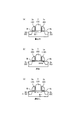
本実施の形態に係る不揮発性半導体記憶装置の構成について、図1を用いて説明する。図1は、実施の形態1に係る不揮発性半導体記憶装置の構成を示す断面図である。本実施の形態に係る不揮発性半導体記憶装置は、ワードゲート3の両側にコントロールゲート5が形成されたツインMONOS構造のメモリである。
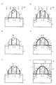
例えば、層間絶縁膜10として、BPSGなどの絶縁膜を成長させる。そして、この層間絶縁膜10上に、フォトレジストを塗布し、パターニングを行って、レジストパターンを形成する。形成したレジストパターンをマスクとして、ドライエッチングにより層間絶縁膜10にコンタクトホールを開口する。そして、このコンタクトホールにタングステンなどの金属を埋め込み、コンタクト11を形成する。続いて、層間絶縁膜10上の全面にアルミなどの導電膜を成膜し、所望のパターニングを行う。これにより、図4(l)に示すように、配線12を形成する。以上のような工程を経て、本実施の形態の不揮発性半導体記憶装置が完成する。
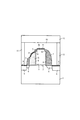
本実施の形態に係る不揮発性半導体記憶装置の構成について、図5を用いて説明する。図5は、実施の形態2に係る不揮発性半導体記憶装置の構成を示す断面図である。実施の形態1では、ツインMONOS構造の不揮発性半導体記憶装置に本発明を適用したが、本実施の形態では、ワードゲート3の片側のみにコントロールゲート5が配設される構造の不揮発性半導体記憶装置に本発明を適用する場合について説明する。
3 ワードゲート、3a 面取り部、3b 突出部、
4 ONO膜、4b 窒化シリコン膜、
5 コントロールゲート、
5o 非選択側コントロールゲート、
5s 選択側コントロールゲート、
6 LDD領域、7 サイドウォール、
8 拡散層、8d ドレイン領域、8s ソース領域、
9 シリサイド層、10 層間絶縁膜、
11 コンタクト、12 配線、
21 レジストパターン、22 LDD注入、
23 ソース・ドレイン注入、24 レジストパターン、
31 ポリシリコン膜、51 ポリシリコン膜
Claims (5)
- 半導体基板上に、第1絶縁膜を介して、一定の幅を有する部分が上に突出した突出部が設けられた形状の第1ゲート電極を形成し、
前記第1ゲート電極の側壁面に第2絶縁膜を介して第2ゲート電極を形成し、
前記第2ゲート電極の側壁面と、前記第1ゲート電極の前記突出部の側壁面とに、絶縁性のサイドウォールを形成し、
前記第1ゲート電極の前記突出部の上面と、前記第2ゲート電極の表面の一部とにシリサイド層を形成し、
前記第1ゲート電極は、
前記第1絶縁膜上に、第1ゲート層を成膜し、
レジストパターンをマスクとして前記第1ゲート層の厚さ方向の一部を等方性エッチングし、
前記等方性エッチングの後、残りの前記第1ゲート層を異方性エッチングすることによって、形成される不揮発性半導体記憶装置の製造方法。 - 前記第2ゲート電極は、前記突出部よりも下側の部分の前記第1ゲート電極の側壁面に形成される請求項1に記載の不揮発性半導体記憶装置の製造方法。
- 前記サイドウォールは、少なくとも、前記第1ゲート電極の側壁面から前記第1ゲート電極の前記第2絶縁膜側の端部上にかけて連続的に形成される請求項1、又は2に記載の不揮発性半導体記憶装置の製造方法。
- 前記サイドウォールが、前記第2ゲート電極上までさらに延在され、前記第1ゲート電極と前記第2ゲート電極の両方に跨って形成されている請求項3に記載の不揮発性半導体記憶装置の製造方法。
- 前記第1ゲート電極の側壁面を含む領域に設けられた前記サイドウォールによって、前記第2ゲート電極の表面の一部に設けられた前記シリサイド層が、前記第1ゲート電極の前記突出部の上面に設けられた前記シリサイド層と絶縁される請求項1乃至4のいずれか1項に記載の不揮発性半導体記憶装置の製造方法。
Priority Applications (2)
| Application Number | Priority Date | Filing Date | Title |
|---|---|---|---|
| JP2009209071A JP5486884B2 (ja) | 2009-09-10 | 2009-09-10 | 不揮発性半導体記憶装置、及びその製造方法 |
| US12/876,376 US8546866B2 (en) | 2009-09-10 | 2010-09-07 | Nonvolatile semiconductor memory device capable of preventing a silicide short |
Applications Claiming Priority (1)
| Application Number | Priority Date | Filing Date | Title |
|---|---|---|---|
| JP2009209071A JP5486884B2 (ja) | 2009-09-10 | 2009-09-10 | 不揮発性半導体記憶装置、及びその製造方法 |
Publications (2)
| Publication Number | Publication Date |
|---|---|
| JP2011060997A JP2011060997A (ja) | 2011-03-24 |
| JP5486884B2 true JP5486884B2 (ja) | 2014-05-07 |
Family
ID=43647035
Family Applications (1)
| Application Number | Title | Priority Date | Filing Date |
|---|---|---|---|
| JP2009209071A Expired - Fee Related JP5486884B2 (ja) | 2009-09-10 | 2009-09-10 | 不揮発性半導体記憶装置、及びその製造方法 |
Country Status (2)
| Country | Link |
|---|---|
| US (1) | US8546866B2 (ja) |
| JP (1) | JP5486884B2 (ja) |
Families Citing this family (8)
| Publication number | Priority date | Publication date | Assignee | Title |
|---|---|---|---|---|
| CN103730341B (zh) * | 2012-10-10 | 2018-02-13 | 中国科学院微电子研究所 | 半导体器件制造方法 |
| JP6026914B2 (ja) * | 2013-02-12 | 2016-11-16 | ルネサスエレクトロニクス株式会社 | 半導体装置の製造方法 |
| JP6081228B2 (ja) * | 2013-02-28 | 2017-02-15 | ルネサスエレクトロニクス株式会社 | 半導体装置およびその製造方法 |
| TW201508753A (zh) * | 2013-08-29 | 2015-03-01 | Chrong-Jung Lin | 記憶體元件、記憶體陣列與其操作方法 |
| US9461055B2 (en) * | 2014-05-16 | 2016-10-04 | Qualcomm Incorporated | Advanced metal-nitride-oxide-silicon multiple-time programmable memory |
| CN108183073A (zh) * | 2016-12-08 | 2018-06-19 | 中芯国际集成电路制造(上海)有限公司 | 半导体结构及其形成方法 |
| CN110854184B (zh) * | 2018-08-03 | 2023-04-07 | 联华电子股份有限公司 | 半导体元件及其制造方法 |
| TWI685085B (zh) * | 2019-02-26 | 2020-02-11 | 華邦電子股份有限公司 | 記憶元件及其製造方法 |
Family Cites Families (5)
| Publication number | Priority date | Publication date | Assignee | Title |
|---|---|---|---|---|
| JP2002231829A (ja) | 2001-01-22 | 2002-08-16 | Halo Lsi Design & Device Technol Inc | 不揮発性半導体メモリおよびその製造方法 |
| US6531350B2 (en) * | 2001-02-22 | 2003-03-11 | Halo, Inc. | Twin MONOS cell fabrication method and array organization |
| JP4746835B2 (ja) * | 2003-10-20 | 2011-08-10 | ルネサスエレクトロニクス株式会社 | 不揮発性半導体記憶装置 |
| JP2009010035A (ja) * | 2007-06-26 | 2009-01-15 | Renesas Technology Corp | 不揮発性半導体記憶装置およびその製造方法 |
| JP2009094170A (ja) * | 2007-10-04 | 2009-04-30 | Nec Electronics Corp | 不揮発性半導体メモリ及びその製造方法 |
-
2009
- 2009-09-10 JP JP2009209071A patent/JP5486884B2/ja not_active Expired - Fee Related
-
2010
- 2010-09-07 US US12/876,376 patent/US8546866B2/en active Active
Also Published As
| Publication number | Publication date |
|---|---|
| US20110057245A1 (en) | 2011-03-10 |
| US8546866B2 (en) | 2013-10-01 |
| JP2011060997A (ja) | 2011-03-24 |
Similar Documents
| Publication | Publication Date | Title |
|---|---|---|
| JP5191633B2 (ja) | 半導体装置およびその製造方法 | |
| JP5734744B2 (ja) | 半導体装置およびその製造方法 | |
| JP5592214B2 (ja) | 半導体装置の製造方法 | |
| JP5486884B2 (ja) | 不揮発性半導体記憶装置、及びその製造方法 | |
| US7268042B2 (en) | Nonvolatile semiconductor memory and making method thereof | |
| TW201907565A (zh) | 半導體裝置 | |
| US10090399B2 (en) | Semiconductor device and a manufacturing method thereof | |
| CN105655339B (zh) | 半导体器件及其制造方法 | |
| JP2009088060A (ja) | 不揮発性半導体記憶装置及びその製造方法 | |
| JP4445353B2 (ja) | 直接トンネル型半導体記憶装置の製造方法 | |
| JP2010245345A (ja) | 不揮発性半導体メモリ及びその製造方法 | |
| JP3958899B2 (ja) | 半導体記憶装置及びその製造方法 | |
| JP5106022B2 (ja) | 不揮発性半導体記憶装置及びその製造方法 | |
| JP2018200936A (ja) | 半導体装置および半導体装置の製造方法 | |
| JP2007335787A (ja) | 不揮発性半導体記憶装置及び不揮発性半導体記憶装置の製造方法 | |
| KR100557531B1 (ko) | 반도체 소자 및 그 제조 방법 | |
| JP2007158093A (ja) | 不揮発性半導体メモリデバイス及びその製造方法 | |
| US10312254B2 (en) | Semiconductor device and a manufacturing method thereof | |
| JP2009194221A (ja) | 半導体装置およびその製造方法 | |
| JP2011210777A (ja) | 半導体装置およびその製造方法 | |
| JP2012094790A (ja) | 半導体装置およびその製造方法 | |
| JP2003243544A (ja) | 不揮発性半導体記憶装置およびその製造方法 | |
| JP2012069652A (ja) | 半導体装置およびその製造方法 | |
| JP5184851B2 (ja) | 不揮発性半導体記憶装置の製造方法 | |
| JP2006080567A (ja) | 半導体集積回路装置およびその製造方法 |
Legal Events
| Date | Code | Title | Description |
|---|---|---|---|
| A621 | Written request for application examination |
Free format text: JAPANESE INTERMEDIATE CODE: A621 Effective date: 20120820 |
|
| A977 | Report on retrieval |
Free format text: JAPANESE INTERMEDIATE CODE: A971007 Effective date: 20131129 |
|
| A131 | Notification of reasons for refusal |
Free format text: JAPANESE INTERMEDIATE CODE: A131 Effective date: 20131203 |
|
| A521 | Request for written amendment filed |
Free format text: JAPANESE INTERMEDIATE CODE: A523 Effective date: 20140124 |
|
| TRDD | Decision of grant or rejection written | ||
| A01 | Written decision to grant a patent or to grant a registration (utility model) |
Free format text: JAPANESE INTERMEDIATE CODE: A01 Effective date: 20140218 |
|
| A61 | First payment of annual fees (during grant procedure) |
Free format text: JAPANESE INTERMEDIATE CODE: A61 Effective date: 20140224 |
|
| R150 | Certificate of patent or registration of utility model |
Ref document number: 5486884 Country of ref document: JP Free format text: JAPANESE INTERMEDIATE CODE: R150 |
|
| S531 | Written request for registration of change of domicile |
Free format text: JAPANESE INTERMEDIATE CODE: R313531 |
|
| R350 | Written notification of registration of transfer |
Free format text: JAPANESE INTERMEDIATE CODE: R350 |
|
| LAPS | Cancellation because of no payment of annual fees |