JP5474323B2 - 電子回路 - Google Patents
電子回路 Download PDFInfo
- Publication number
- JP5474323B2 JP5474323B2 JP2008216248A JP2008216248A JP5474323B2 JP 5474323 B2 JP5474323 B2 JP 5474323B2 JP 2008216248 A JP2008216248 A JP 2008216248A JP 2008216248 A JP2008216248 A JP 2008216248A JP 5474323 B2 JP5474323 B2 JP 5474323B2
- Authority
- JP
- Japan
- Prior art keywords
- coil
- pulse
- circuit
- transmission
- data
- Prior art date
- Legal status (The legal status is an assumption and is not a legal conclusion. Google has not performed a legal analysis and makes no representation as to the accuracy of the status listed.)
- Active
Links
- 230000005540 biological transmission Effects 0.000 claims description 144
- 230000008859 change Effects 0.000 claims description 29
- 239000000758 substrate Substances 0.000 claims description 17
- 238000000034 method Methods 0.000 claims description 16
- 230000008569 process Effects 0.000 claims description 2
- 239000004065 semiconductor Substances 0.000 description 16
- 238000010586 diagram Methods 0.000 description 13
- 230000006854 communication Effects 0.000 description 11
- 238000004891 communication Methods 0.000 description 11
- 230000001939 inductive effect Effects 0.000 description 9
- 230000008878 coupling Effects 0.000 description 8
- 238000010168 coupling process Methods 0.000 description 8
- 238000005859 coupling reaction Methods 0.000 description 8
- 230000004044 response Effects 0.000 description 6
- 230000001360 synchronised effect Effects 0.000 description 5
- 238000001514 detection method Methods 0.000 description 4
- 230000007423 decrease Effects 0.000 description 3
- 230000000630 rising effect Effects 0.000 description 3
- 230000035945 sensitivity Effects 0.000 description 3
- 230000009471 action Effects 0.000 description 2
- 230000000694 effects Effects 0.000 description 2
- 238000005516 engineering process Methods 0.000 description 2
- 230000007257 malfunction Effects 0.000 description 2
- 230000007175 bidirectional communication Effects 0.000 description 1
- 230000000052 comparative effect Effects 0.000 description 1
- 230000000295 complement effect Effects 0.000 description 1
- 230000010354 integration Effects 0.000 description 1
- 230000007246 mechanism Effects 0.000 description 1
- 230000003071 parasitic effect Effects 0.000 description 1
- 230000003252 repetitive effect Effects 0.000 description 1
- 230000008054 signal transmission Effects 0.000 description 1
- 230000011664 signaling Effects 0.000 description 1
Images


Classifications
-
- H—ELECTRICITY
- H04—ELECTRIC COMMUNICATION TECHNIQUE
- H04L—TRANSMISSION OF DIGITAL INFORMATION, e.g. TELEGRAPHIC COMMUNICATION
- H04L25/00—Baseband systems
- H04L25/38—Synchronous or start-stop systems, e.g. for Baudot code
- H04L25/40—Transmitting circuits; Receiving circuits
- H04L25/49—Transmitting circuits; Receiving circuits using code conversion at the transmitter; using predistortion; using insertion of idle bits for obtaining a desired frequency spectrum; using three or more amplitude levels ; Baseband coding techniques specific to data transmission systems
- H04L25/493—Transmitting circuits; Receiving circuits using code conversion at the transmitter; using predistortion; using insertion of idle bits for obtaining a desired frequency spectrum; using three or more amplitude levels ; Baseband coding techniques specific to data transmission systems by transition coding, i.e. the time-position or direction of a transition being encoded before transmission
-
- H—ELECTRICITY
- H04—ELECTRIC COMMUNICATION TECHNIQUE
- H04L—TRANSMISSION OF DIGITAL INFORMATION, e.g. TELEGRAPHIC COMMUNICATION
- H04L25/00—Baseband systems
- H04L25/02—Details ; arrangements for supplying electrical power along data transmission lines
- H04L25/0264—Arrangements for coupling to transmission lines
- H04L25/0266—Arrangements for providing Galvanic isolation, e.g. by means of magnetic or capacitive coupling
-
- H—ELECTRICITY
- H04—ELECTRIC COMMUNICATION TECHNIQUE
- H04L—TRANSMISSION OF DIGITAL INFORMATION, e.g. TELEGRAPHIC COMMUNICATION
- H04L25/00—Baseband systems
- H04L25/02—Details ; arrangements for supplying electrical power along data transmission lines
- H04L25/06—Dc level restoring means; Bias distortion correction ; Decision circuits providing symbol by symbol detection
- H04L25/061—Dc level restoring means; Bias distortion correction ; Decision circuits providing symbol by symbol detection providing hard decisions only; arrangements for tracking or suppressing unwanted low frequency components, e.g. removal of dc offset
-
- H—ELECTRICITY
- H04—ELECTRIC COMMUNICATION TECHNIQUE
- H04L—TRANSMISSION OF DIGITAL INFORMATION, e.g. TELEGRAPHIC COMMUNICATION
- H04L25/00—Baseband systems
- H04L25/38—Synchronous or start-stop systems, e.g. for Baudot code
- H04L25/40—Transmitting circuits; Receiving circuits
Landscapes
- Engineering & Computer Science (AREA)
- Computer Networks & Wireless Communication (AREA)
- Signal Processing (AREA)
- Power Engineering (AREA)
- Physics & Mathematics (AREA)
- Spectroscopy & Molecular Physics (AREA)
- Near-Field Transmission Systems (AREA)
- Electronic Switches (AREA)
Description
先ず、本願において開示される発明の代表的な実施の形態について概要を説明する。代表的な実施の形態についての概要説明で括弧を付して参照する図面中の参照符号はそれが付された構成要素の概念に含まれるものを例示するに過ぎない。
実施の形態について更に詳述する。以下、本発明を実施するための形態を図面に基づいて詳細に説明する。なお、発明を実施するための形態を説明するための全図において、同一の機能を有する要素には同一の符号を付して、その繰り返しの説明を省略する。
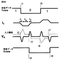
図1Aには本発明に係る電子回路の第1の実施の形態が示される。図1Bはその動作波形を示す。本発明の電子回路は第1半導体チップ1と第2半導体チップ2が積層され、相互間で誘導結合による近接非接触通信を行う機能を有する。前記非接触通信機能を実現するための単位ユニットとして例えば半導体チップ1はコイル10と送信回路11を有し、半導体チップ2はコイル20と受信回路21を有する。特に図示はしないが、例えば上記単位ユニットは、送受信データの並列ビット数分と、送受信データのビット同期のための1本のストローブ信号の分が設けられる。ストローブ信号は送受信データのビット同期で論理値が変化する信号とされる。したがって、第2半導体チップはストローブ信号とデータを受信することによって受信データの先頭を認識してビット単位で受信データを識別する。
図5には本発明に係る電子回路の第2の実施の形態が示される。本発明の電子回路は第1半導体チップ1Aと第2半導体チップ2Aが積層され、相互間で誘導結合による近接非接触通信を行う機能を有する。前記非接触通信機能を実現するための単位ユニットとして例えば半導体チップ1Aはコイル10Aと送信回路11Aを有し、半導体チップ2Aはコイル20Aと受信回路21Aを有する。特に図示はしないが、例えば上記単位ユニットは、送受信データの並列ビット数分と、送受信データのビット同期のための1本のストローブ信号の分が設けられる。ストローブ信号は送受信データのビット同期で論理値が変化する信号とされる。したがって、第2半導体チップはストローブ信号とデータを受信することによって受信データの先頭を認識してビット単位で受信データを識別する。
2、2A 半導体チップ
10、10A 送信用のコイル
11、11A 送信回路
20、20A 受信用のコイル
21、21A 受信回路
22,22A ヒステリシス比較器
23 フリップフロップ(順序回路)
N5、P7 初期化用のMOSトランジスタ
25 制御回路
Claims (7)
- 第1コイル、及びパケット毎に先頭が既定の論理値とされる送信データの論理値の変化毎に前記第1コイルに第1方向のパルス電流を流す送信回路を有する第1基板と、
前記第1コイルに誘導結合する第2コイル、及び前記第2コイルに接続された受信回路を有する第2基板と、を備え、
前記受信回路は、前記第1方向のパルス電流によって第2コイルに誘導されるダブルパルス形状の誘導電圧を閾値電圧を用いて判定して単一極性でシングルパルス信号を出力する比較器、及び前記シングルパルス信号を入力する毎に出力を反転させる順序回路を有し、
前記比較器はその出力を所定の論理値に初期化するための初期化スイッチを有し、
更に、前記パケットの先頭毎に前記初期化スイッチの初期化動作を行う第1制御回路を有する、電子回路。 - 前記比較器は、ヒステリシス特性を有する入力の閾値電圧に基づいて前記ダブルパルス形状の誘導電圧を判定し、その出力信号の論理値が反転する毎に前記閾値電圧が変化する、請求項1記載の電子回路。
- 前記第1制御回路は、前記初期化スイッチの初期化動作によって前記比較器の入力の閾値電圧を2つの値の内の一方に初期化する、請求項2記載の電子回路。
- 前記送信回路は、送信データの遅延回路と、
前記送信データと前記遅延回路の出力とを入力する排他的論理和ゲートと、
前記排他的論理和ゲートの一致出力で前記第1コイルに一方向の電流を流し、前記排他的論理和ゲートの不一致出力で前記第1コイルに一方向の電流が流れるのを抑止する駆動回路とを有する、請求項3記載の電子回路。 - 前記比較器は、前記第2コイルの一端に結合された第1CMOSインバータと、
前記第2コイルの他端に結合された第2CMOSインバータと、
前記第1CMOSインバータのpチャンネル型MOSトランジスタに並列接続され且つゲートが前記第2CMOSインバータの出力端子に結合された第1ラッチ用pチャンネル型MOSトランジスタと、
前記第2CMOSインバータのpチャンネル型MOSトランジスタに並列接続され且つゲートが前記第1CMOSインバータの出力端子に結合された第2ラッチ用pチャンネル型MOSトランジスタと、
前記第1CMOSトランジスタの出力端子にドレインが接続され且つゲートに第1制御回路からの初期化動作信号が供給される初期化スイッチMOSトランジスタとを有し、
前記第1CMOSトランジスタの出力端子が比較器の出力端子とされる、請求項3記載の電子回路。 - 前記第1基板は更に、第3コイル及び先頭が既定の論理値とされる送信データの論理値の変化に応じて異なる方向のパルス電流を前記第3コイルに流す第3コイル用送信回路を有し、
前記第2基板は更に、前記第3コイルに誘導結合する第4コイル、及び前記第4コイルに接続された第4コイル用受信回路を有し、
前記第3コイル用送信回路は、前記パルス電流のパルス幅を決定し、
前記パルス幅は前記パルス電流の変化率に従って第4コイルに誘導される誘導電圧を双極性の一対のシングルパルス形状とするために必要な幅を有し、
前記第4コイル用受信回路は、前記シングルパルス形状の誘導電圧を判定して出力するヒステリシス比較器を有する請求項1記載の電子回路。 - 前記第1基板は更に、第3コイル及び送信データの論理値の変化に応じて前記第3コイルに異なる方向のパルス電流を流す第3コイル用送信回路を有し、
前記第2基板は更に、前記第3コイルに誘導結合する第4コイル、前記第4コイルに接続された第4コイル用受信回路、及び前記受信回路による受信データを処理する第2制御回路を有し、
前記第3コイル用送信回路は、遅延素子による遅延時間に基づいて前記パルス電流のパルス幅を決定し、
前記パルス幅は前記パルス電流の変化率に従って第4コイルに誘導される誘導電圧を双極性の一対のシングルパルス形状とするために必要な幅を有し、
前記第4コイル用受信回路は、前記シングルパルス形状の誘導電圧を判定して出力するヒステリシス比較器を有し、
前記送信データは先頭に論理値が相違する2ビットのダミーデータを有し、
前記第2制御回路は受信データの先頭の2ビットを無視する、請求項1記載の電子回路。
Priority Applications (4)
| Application Number | Priority Date | Filing Date | Title |
|---|---|---|---|
| JP2008216248A JP5474323B2 (ja) | 2008-08-26 | 2008-08-26 | 電子回路 |
| PCT/JP2009/003711 WO2010023825A1 (ja) | 2008-08-26 | 2009-08-04 | 電子回路 |
| KR1020117004608A KR101548780B1 (ko) | 2008-08-26 | 2009-08-04 | 전자 회로 |
| US13/061,128 US8933590B2 (en) | 2008-08-26 | 2009-08-04 | Electronic circuit |
Applications Claiming Priority (1)
| Application Number | Priority Date | Filing Date | Title |
|---|---|---|---|
| JP2008216248A JP5474323B2 (ja) | 2008-08-26 | 2008-08-26 | 電子回路 |
Publications (2)
| Publication Number | Publication Date |
|---|---|
| JP2010056593A JP2010056593A (ja) | 2010-03-11 |
| JP5474323B2 true JP5474323B2 (ja) | 2014-04-16 |
Family
ID=41721009
Family Applications (1)
| Application Number | Title | Priority Date | Filing Date |
|---|---|---|---|
| JP2008216248A Active JP5474323B2 (ja) | 2008-08-26 | 2008-08-26 | 電子回路 |
Country Status (4)
| Country | Link |
|---|---|
| US (1) | US8933590B2 (ja) |
| JP (1) | JP5474323B2 (ja) |
| KR (1) | KR101548780B1 (ja) |
| WO (1) | WO2010023825A1 (ja) |
Families Citing this family (19)
| Publication number | Priority date | Publication date | Assignee | Title |
|---|---|---|---|---|
| US8068011B1 (en) | 2010-08-27 | 2011-11-29 | Q Street, LLC | System and method for interactive user-directed interfacing between handheld devices and RFID media |
| JP5698624B2 (ja) * | 2011-08-22 | 2015-04-08 | 学校法人慶應義塾 | 小振幅差動パルス送信回路 |
| KR101433028B1 (ko) * | 2012-05-03 | 2014-08-21 | 서강대학교산학협력단 | 케이블에 의한 신호 왜곡을 개선하는 아날로그 신호 보정 회로 |
| BR112014027491B1 (pt) | 2012-05-03 | 2022-07-12 | Atlas Copco Industrial Technique Ab | Sistema de transmissão, ferramenta de potência e método para transmissão sem fio |
| JP5796558B2 (ja) * | 2012-09-05 | 2015-10-21 | 株式会社豊田自動織機 | 紡機の糸検出装置 |
| JP5832398B2 (ja) * | 2012-09-10 | 2015-12-16 | ルネサスエレクトロニクス株式会社 | 信号伝送回路 |
| KR102048443B1 (ko) | 2012-09-24 | 2020-01-22 | 삼성전자주식회사 | 근거리 무선 송수신 방법 및 장치 |
| DE112012007198B4 (de) | 2012-12-04 | 2021-08-26 | Mitsubishi Electric Corporation | Signalübertragungsschaltung |
| US9294151B2 (en) | 2012-12-12 | 2016-03-22 | Oceaneering International, Inc. | Wireless data transmission via inductive coupling using di/dt as the magnetic modulation scheme and hysteresis |
| US9577637B2 (en) * | 2014-02-19 | 2017-02-21 | Altera Corporation | Stability-enhanced physically unclonable function circuitry |
| JP6495671B2 (ja) * | 2015-01-28 | 2019-04-03 | 東芝メモリ株式会社 | 送信回路及び通信システム |
| US20160359004A1 (en) * | 2015-06-03 | 2016-12-08 | Veeco Instruments, Inc. | Stress control for heteroepitaxy |
| US10615850B2 (en) * | 2016-02-18 | 2020-04-07 | Ultramemory Inc. | Layered semiconductor device and data communication method |
| KR102587728B1 (ko) * | 2016-10-07 | 2023-10-12 | 삼성디스플레이 주식회사 | 박막 트랜지스터 어레이 기판 및 그의 제조방법 |
| EP3370082B1 (en) | 2017-03-02 | 2020-12-09 | Nxp B.V. | Processing module and associated method |
| EP3370083B1 (en) * | 2017-03-02 | 2020-08-26 | Nxp B.V. | Processing module and associated method |
| EP3370464B1 (en) | 2017-03-02 | 2020-02-26 | Nxp B.V. | Processing module and associated method |
| EP3370365B1 (en) | 2017-03-02 | 2020-07-01 | Nxp B.V. | Processing module and associated method |
| US10868528B2 (en) | 2017-09-08 | 2020-12-15 | Ultramemory Inc. | Signal output device |
Family Cites Families (9)
| Publication number | Priority date | Publication date | Assignee | Title |
|---|---|---|---|---|
| JPH05308244A (ja) * | 1992-04-28 | 1993-11-19 | Shimadzu Corp | 信号伝送回路 |
| JPH0823310A (ja) | 1994-07-11 | 1996-01-23 | Fuji Electric Co Ltd | 光信号伝送装置 |
| US5952849A (en) * | 1997-02-21 | 1999-09-14 | Analog Devices, Inc. | Logic isolator with high transient immunity |
| US6262600B1 (en) * | 2000-02-14 | 2001-07-17 | Analog Devices, Inc. | Isolator for transmitting logic signals across an isolation barrier |
| FR2808942B1 (fr) * | 2000-05-12 | 2002-08-16 | St Microelectronics Sa | Validation de la presence d'un transpondeur electromagnetique dans le champ d'un lecteur a demodulation de phase |
| US7060030B2 (en) * | 2002-01-08 | 2006-06-13 | Cardiac Pacemakers, Inc. | Two-hop telemetry interface for medical device |
| EP2302850A1 (en) * | 2003-04-30 | 2011-03-30 | Analog Devices, Inc. | Signal isolators using micro-transformers |
| JP4131544B2 (ja) * | 2004-02-13 | 2008-08-13 | 学校法人慶應義塾 | 電子回路 |
| JP4600458B2 (ja) | 2007-10-16 | 2010-12-15 | 株式会社三洋物産 | 遊技機 |
-
2008
- 2008-08-26 JP JP2008216248A patent/JP5474323B2/ja active Active
-
2009
- 2009-08-04 US US13/061,128 patent/US8933590B2/en active Active
- 2009-08-04 WO PCT/JP2009/003711 patent/WO2010023825A1/ja active Application Filing
- 2009-08-04 KR KR1020117004608A patent/KR101548780B1/ko active IP Right Grant
Also Published As
| Publication number | Publication date |
|---|---|
| US8933590B2 (en) | 2015-01-13 |
| JP2010056593A (ja) | 2010-03-11 |
| WO2010023825A1 (ja) | 2010-03-04 |
| KR20110045025A (ko) | 2011-05-03 |
| US20120007438A1 (en) | 2012-01-12 |
| KR101548780B1 (ko) | 2015-09-11 |
Similar Documents
| Publication | Publication Date | Title |
|---|---|---|
| JP5474323B2 (ja) | 電子回路 | |
| JP6185171B2 (ja) | 多相クロック生成方法 | |
| EP1064767B1 (en) | High speed signaling for interfacing vlsi cmos circuits | |
| JP3189815B2 (ja) | 入力回路、出力回路、入出力回路、及び入力信号処理方法 | |
| JP5600237B2 (ja) | 集積回路 | |
| US7778374B2 (en) | Dual reference input receiver of semiconductor device and method of receiving input data signal | |
| US7471110B2 (en) | Current mode interface for off-chip high speed communication | |
| JP2009049672A (ja) | 差動送信回路、差動受信回路、信号伝送回路および信号伝送システム | |
| US20160285453A1 (en) | Driver using pull-up nmos transistor | |
| JP2008113196A (ja) | 信号検知回路 | |
| US7079589B1 (en) | Serial digital communication superimposed on a digital signal over a single wire | |
| US9240789B2 (en) | Sub-rate low-swing data receiver | |
| US7629813B2 (en) | Dynamic refreshed receiver for proximity communication | |
| JP2007329898A (ja) | 信号変換回路 | |
| TW201421251A (zh) | 傳輸器電路、接收器電路及傳輸/接收系統 | |
| KR101759681B1 (ko) | 다중-위상 시그널링을 위한 클록 펄스 생성기 | |
| US7518411B2 (en) | Data receiving apparatus using semi-dual reference voltage | |
| US9524763B2 (en) | Source-synchronous data transmission with non-uniform interface topology | |
| US8922251B2 (en) | Buffer control circuit and integrated circuit including the same | |
| JP2011066515A (ja) | 集積回路 | |
| US7248083B2 (en) | Methods and systems for decreasing transmission timing variations | |
| KR20090006577A (ko) | 반도체메모리소자의 입력 버퍼 | |
| US20040037362A1 (en) | Controlled frequency signals | |
| US7145483B2 (en) | Chip to chip interface for encoding data and clock signals | |
| KR100508722B1 (ko) | 펄스폭 고정 장치 |
Legal Events
| Date | Code | Title | Description |
|---|---|---|---|
| A621 | Written request for application examination |
Free format text: JAPANESE INTERMEDIATE CODE: A621 Effective date: 20110801 |
|
| A131 | Notification of reasons for refusal |
Free format text: JAPANESE INTERMEDIATE CODE: A131 Effective date: 20130321 |
|
| A131 | Notification of reasons for refusal |
Free format text: JAPANESE INTERMEDIATE CODE: A131 Effective date: 20130711 |
|
| A521 | Request for written amendment filed |
Free format text: JAPANESE INTERMEDIATE CODE: A523 Effective date: 20130904 |
|
| TRDD | Decision of grant or rejection written | ||
| A01 | Written decision to grant a patent or to grant a registration (utility model) |
Free format text: JAPANESE INTERMEDIATE CODE: A01 Effective date: 20140130 |
|
| A61 | First payment of annual fees (during grant procedure) |
Free format text: JAPANESE INTERMEDIATE CODE: A61 Effective date: 20140205 |
|
| R150 | Certificate of patent or registration of utility model |
Ref document number: 5474323 Country of ref document: JP Free format text: JAPANESE INTERMEDIATE CODE: R150 Free format text: JAPANESE INTERMEDIATE CODE: R150 |
|
| S111 | Request for change of ownership or part of ownership |
Free format text: JAPANESE INTERMEDIATE CODE: R313113 |
|
| R350 | Written notification of registration of transfer |
Free format text: JAPANESE INTERMEDIATE CODE: R350 |
|
| R250 | Receipt of annual fees |
Free format text: JAPANESE INTERMEDIATE CODE: R250 |
|
| R250 | Receipt of annual fees |
Free format text: JAPANESE INTERMEDIATE CODE: R250 |
|
| R250 | Receipt of annual fees |
Free format text: JAPANESE INTERMEDIATE CODE: R250 |
|
| R250 | Receipt of annual fees |
Free format text: JAPANESE INTERMEDIATE CODE: R250 |
|
| R250 | Receipt of annual fees |
Free format text: JAPANESE INTERMEDIATE CODE: R250 |
|
| R250 | Receipt of annual fees |
Free format text: JAPANESE INTERMEDIATE CODE: R250 |
|
| R250 | Receipt of annual fees |
Free format text: JAPANESE INTERMEDIATE CODE: R250 |
|
| R250 | Receipt of annual fees |
Free format text: JAPANESE INTERMEDIATE CODE: R250 |