JP5458323B2 - Electrostatic chuck and manufacturing method thereof - Google Patents
Electrostatic chuck and manufacturing method thereof Download PDFInfo
- Publication number
- JP5458323B2 JP5458323B2 JP2010533896A JP2010533896A JP5458323B2 JP 5458323 B2 JP5458323 B2 JP 5458323B2 JP 2010533896 A JP2010533896 A JP 2010533896A JP 2010533896 A JP2010533896 A JP 2010533896A JP 5458323 B2 JP5458323 B2 JP 5458323B2
- Authority
- JP
- Japan
- Prior art keywords
- substrate
- electrostatic chuck
- elastic
- convex portion
- rubber
- Prior art date
- Legal status (The legal status is an assumption and is not a legal conclusion. Google has not performed a legal analysis and makes no representation as to the accuracy of the status listed.)
- Active
Links
- 238000004519 manufacturing process Methods 0.000 title claims description 23
- 239000000758 substrate Substances 0.000 claims description 111
- 238000001179 sorption measurement Methods 0.000 claims description 76
- 239000013013 elastic material Substances 0.000 claims description 18
- 238000000034 method Methods 0.000 claims description 15
- 229920002379 silicone rubber Polymers 0.000 claims description 6
- 239000004945 silicone rubber Substances 0.000 claims description 5
- 229920001973 fluoroelastomer Polymers 0.000 claims description 3
- 229920000181 Ethylene propylene rubber Polymers 0.000 claims description 2
- 229920000459 Nitrile rubber Polymers 0.000 claims description 2
- 239000005062 Polybutadiene Substances 0.000 claims description 2
- 229920006311 Urethane elastomer Polymers 0.000 claims description 2
- 229920000800 acrylic rubber Polymers 0.000 claims description 2
- 229920005549 butyl rubber Polymers 0.000 claims description 2
- 229920005558 epichlorohydrin rubber Polymers 0.000 claims description 2
- 229920003049 isoprene rubber Polymers 0.000 claims description 2
- 229920001084 poly(chloroprene) Polymers 0.000 claims description 2
- 229920000058 polyacrylate Polymers 0.000 claims description 2
- 229920002857 polybutadiene Polymers 0.000 claims description 2
- 229920003048 styrene butadiene rubber Polymers 0.000 claims description 2
- 235000012431 wafers Nutrition 0.000 description 25
- 239000011521 glass Substances 0.000 description 18
- 239000004065 semiconductor Substances 0.000 description 16
- 239000000463 material Substances 0.000 description 13
- 239000004642 Polyimide Substances 0.000 description 11
- 235000014443 Pyrus communis Nutrition 0.000 description 11
- 229920001721 polyimide Polymers 0.000 description 11
- 229910052710 silicon Inorganic materials 0.000 description 10
- 239000010703 silicon Substances 0.000 description 10
- XUIMIQQOPSSXEZ-UHFFFAOYSA-N Silicon Chemical compound [Si] XUIMIQQOPSSXEZ-UHFFFAOYSA-N 0.000 description 9
- 238000001816 cooling Methods 0.000 description 9
- 229920001971 elastomer Polymers 0.000 description 8
- 239000002245 particle Substances 0.000 description 8
- 229920001296 polysiloxane Polymers 0.000 description 8
- 239000005060 rubber Substances 0.000 description 8
- RYGMFSIKBFXOCR-UHFFFAOYSA-N Copper Chemical compound [Cu] RYGMFSIKBFXOCR-UHFFFAOYSA-N 0.000 description 7
- 239000000356 contaminant Substances 0.000 description 6
- 239000002390 adhesive tape Substances 0.000 description 5
- 239000000919 ceramic Substances 0.000 description 5
- 239000011889 copper foil Substances 0.000 description 5
- 238000005468 ion implantation Methods 0.000 description 5
- 229920003223 poly(pyromellitimide-1,4-diphenyl ether) Polymers 0.000 description 5
- 238000012545 processing Methods 0.000 description 5
- 239000011347 resin Substances 0.000 description 5
- 229920005989 resin Polymers 0.000 description 5
- 239000004593 Epoxy Substances 0.000 description 4
- XAGFODPZIPBFFR-UHFFFAOYSA-N aluminium Chemical compound [Al] XAGFODPZIPBFFR-UHFFFAOYSA-N 0.000 description 4
- 230000008602 contraction Effects 0.000 description 4
- 238000005530 etching Methods 0.000 description 4
- 229910052782 aluminium Inorganic materials 0.000 description 3
- 238000011109 contamination Methods 0.000 description 3
- 239000000498 cooling water Substances 0.000 description 3
- 230000000694 effects Effects 0.000 description 3
- 238000005516 engineering process Methods 0.000 description 3
- 239000004973 liquid crystal related substance Substances 0.000 description 3
- 229910052751 metal Inorganic materials 0.000 description 3
- 239000002184 metal Substances 0.000 description 3
- 239000013464 silicone adhesive Substances 0.000 description 3
- RZVAJINKPMORJF-UHFFFAOYSA-N Acetaminophen Chemical compound CC(=O)NC1=CC=C(O)C=C1 RZVAJINKPMORJF-UHFFFAOYSA-N 0.000 description 2
- NIXOWILDQLNWCW-UHFFFAOYSA-N acrylic acid group Chemical group C(C=C)(=O)O NIXOWILDQLNWCW-UHFFFAOYSA-N 0.000 description 2
- PNEYBMLMFCGWSK-UHFFFAOYSA-N aluminium oxide Inorganic materials [O-2].[O-2].[O-2].[Al+3].[Al+3] PNEYBMLMFCGWSK-UHFFFAOYSA-N 0.000 description 2
- 239000002131 composite material Substances 0.000 description 2
- 229910052802 copper Inorganic materials 0.000 description 2
- 239000010949 copper Substances 0.000 description 2
- 238000010586 diagram Methods 0.000 description 2
- 238000002474 experimental method Methods 0.000 description 2
- 238000002513 implantation Methods 0.000 description 2
- 238000009413 insulation Methods 0.000 description 2
- 238000010884 ion-beam technique Methods 0.000 description 2
- 239000005297 pyrex Substances 0.000 description 2
- 238000012360 testing method Methods 0.000 description 2
- 239000010409 thin film Substances 0.000 description 2
- 238000012546 transfer Methods 0.000 description 2
- 241001272720 Medialuna californiensis Species 0.000 description 1
- 230000015572 biosynthetic process Effects 0.000 description 1
- 238000005422 blasting Methods 0.000 description 1
- 239000011248 coating agent Substances 0.000 description 1
- 238000000576 coating method Methods 0.000 description 1
- 230000000052 comparative effect Effects 0.000 description 1
- 230000006835 compression Effects 0.000 description 1
- 238000007906 compression Methods 0.000 description 1
- 239000002826 coolant Substances 0.000 description 1
- 230000007423 decrease Effects 0.000 description 1
- 238000007872 degassing Methods 0.000 description 1
- 238000013461 design Methods 0.000 description 1
- 229920006351 engineering plastic Polymers 0.000 description 1
- 239000010408 film Substances 0.000 description 1
- 239000012467 final product Substances 0.000 description 1
- 239000011888 foil Substances 0.000 description 1
- 238000010438 heat treatment Methods 0.000 description 1
- 238000011835 investigation Methods 0.000 description 1
- 238000005259 measurement Methods 0.000 description 1
- 238000000465 moulding Methods 0.000 description 1
- 238000005457 optimization Methods 0.000 description 1
- 230000008520 organization Effects 0.000 description 1
- 239000013500 performance material Substances 0.000 description 1
- 239000000843 powder Substances 0.000 description 1
- 239000000047 product Substances 0.000 description 1
- 239000003507 refrigerant Substances 0.000 description 1
- 150000003376 silicon Chemical class 0.000 description 1
- 239000011856 silicon-based particle Substances 0.000 description 1
- 229910001220 stainless steel Inorganic materials 0.000 description 1
- 239000010935 stainless steel Substances 0.000 description 1
- 230000003068 static effect Effects 0.000 description 1
- 239000000126 substance Substances 0.000 description 1
- 229920003051 synthetic elastomer Polymers 0.000 description 1
- 239000005061 synthetic rubber Substances 0.000 description 1
- 238000010998 test method Methods 0.000 description 1
- 238000007740 vapor deposition Methods 0.000 description 1
- 239000012808 vapor phase Substances 0.000 description 1
- 230000000007 visual effect Effects 0.000 description 1
Images


Classifications
-
- H—ELECTRICITY
- H01—ELECTRIC ELEMENTS
- H01L—SEMICONDUCTOR DEVICES NOT COVERED BY CLASS H10
- H01L21/00—Processes or apparatus adapted for the manufacture or treatment of semiconductor or solid state devices or of parts thereof
- H01L21/67—Apparatus specially adapted for handling semiconductor or electric solid state devices during manufacture or treatment thereof; Apparatus specially adapted for handling wafers during manufacture or treatment of semiconductor or electric solid state devices or components ; Apparatus not specifically provided for elsewhere
- H01L21/683—Apparatus specially adapted for handling semiconductor or electric solid state devices during manufacture or treatment thereof; Apparatus specially adapted for handling wafers during manufacture or treatment of semiconductor or electric solid state devices or components ; Apparatus not specifically provided for elsewhere for supporting or gripping
- H01L21/6831—Apparatus specially adapted for handling semiconductor or electric solid state devices during manufacture or treatment thereof; Apparatus specially adapted for handling wafers during manufacture or treatment of semiconductor or electric solid state devices or components ; Apparatus not specifically provided for elsewhere for supporting or gripping using electrostatic chucks
-
- B—PERFORMING OPERATIONS; TRANSPORTING
- B23—MACHINE TOOLS; METAL-WORKING NOT OTHERWISE PROVIDED FOR
- B23Q—DETAILS, COMPONENTS, OR ACCESSORIES FOR MACHINE TOOLS, e.g. ARRANGEMENTS FOR COPYING OR CONTROLLING; MACHINE TOOLS IN GENERAL CHARACTERISED BY THE CONSTRUCTION OF PARTICULAR DETAILS OR COMPONENTS; COMBINATIONS OR ASSOCIATIONS OF METAL-WORKING MACHINES, NOT DIRECTED TO A PARTICULAR RESULT
- B23Q3/00—Devices holding, supporting, or positioning work or tools, of a kind normally removable from the machine
- B23Q3/15—Devices for holding work using magnetic or electric force acting directly on the work
-
- H—ELECTRICITY
- H01—ELECTRIC ELEMENTS
- H01L—SEMICONDUCTOR DEVICES NOT COVERED BY CLASS H10
- H01L21/00—Processes or apparatus adapted for the manufacture or treatment of semiconductor or solid state devices or of parts thereof
- H01L21/67—Apparatus specially adapted for handling semiconductor or electric solid state devices during manufacture or treatment thereof; Apparatus specially adapted for handling wafers during manufacture or treatment of semiconductor or electric solid state devices or components ; Apparatus not specifically provided for elsewhere
- H01L21/683—Apparatus specially adapted for handling semiconductor or electric solid state devices during manufacture or treatment thereof; Apparatus specially adapted for handling wafers during manufacture or treatment of semiconductor or electric solid state devices or components ; Apparatus not specifically provided for elsewhere for supporting or gripping
- H01L21/6831—Apparatus specially adapted for handling semiconductor or electric solid state devices during manufacture or treatment thereof; Apparatus specially adapted for handling wafers during manufacture or treatment of semiconductor or electric solid state devices or components ; Apparatus not specifically provided for elsewhere for supporting or gripping using electrostatic chucks
- H01L21/6833—Details of electrostatic chucks
-
- H—ELECTRICITY
- H01—ELECTRIC ELEMENTS
- H01L—SEMICONDUCTOR DEVICES NOT COVERED BY CLASS H10
- H01L21/00—Processes or apparatus adapted for the manufacture or treatment of semiconductor or solid state devices or of parts thereof
- H01L21/67—Apparatus specially adapted for handling semiconductor or electric solid state devices during manufacture or treatment thereof; Apparatus specially adapted for handling wafers during manufacture or treatment of semiconductor or electric solid state devices or components ; Apparatus not specifically provided for elsewhere
- H01L21/683—Apparatus specially adapted for handling semiconductor or electric solid state devices during manufacture or treatment thereof; Apparatus specially adapted for handling wafers during manufacture or treatment of semiconductor or electric solid state devices or components ; Apparatus not specifically provided for elsewhere for supporting or gripping
- H01L21/687—Apparatus specially adapted for handling semiconductor or electric solid state devices during manufacture or treatment thereof; Apparatus specially adapted for handling wafers during manufacture or treatment of semiconductor or electric solid state devices or components ; Apparatus not specifically provided for elsewhere for supporting or gripping using mechanical means, e.g. chucks, clamps or pinches
- H01L21/68714—Apparatus specially adapted for handling semiconductor or electric solid state devices during manufacture or treatment thereof; Apparatus specially adapted for handling wafers during manufacture or treatment of semiconductor or electric solid state devices or components ; Apparatus not specifically provided for elsewhere for supporting or gripping using mechanical means, e.g. chucks, clamps or pinches the wafers being placed on a susceptor, stage or support
- H01L21/6875—Apparatus specially adapted for handling semiconductor or electric solid state devices during manufacture or treatment thereof; Apparatus specially adapted for handling wafers during manufacture or treatment of semiconductor or electric solid state devices or components ; Apparatus not specifically provided for elsewhere for supporting or gripping using mechanical means, e.g. chucks, clamps or pinches the wafers being placed on a susceptor, stage or support characterised by a plurality of individual support members, e.g. support posts or protrusions
-
- H—ELECTRICITY
- H02—GENERATION; CONVERSION OR DISTRIBUTION OF ELECTRIC POWER
- H02N—ELECTRIC MACHINES NOT OTHERWISE PROVIDED FOR
- H02N13/00—Clutches or holding devices using electrostatic attraction, e.g. using Johnson-Rahbek effect
Description
この発明は、液晶パネル製造に使用される基板貼り合せ装置やイオンドーピング装置等に具備されてガラス基板を吸着・保持したり、また、半導体素子製造プロセスで用いられているエッチング処理、化学気相蒸着(CVD)による薄膜形成などのプラズマ処理装置、電子露光装置、イオン描写装置、イオン注入装置等に具備されて半導体ウエハを吸着・保持するのに使用される静電チャックに関する。 The present invention is provided in a substrate bonding apparatus or an ion doping apparatus used for manufacturing a liquid crystal panel, and adsorbs and holds a glass substrate, and also performs an etching process or a chemical vapor phase used in a semiconductor element manufacturing process. The present invention relates to an electrostatic chuck that is provided in a plasma processing apparatus such as thin film formation by vapor deposition (CVD), an electronic exposure apparatus, an ion drawing apparatus, an ion implantation apparatus, and the like and is used to attract and hold a semiconductor wafer.
静電チャックは、上記のような種々の半導体製造装置や液晶パネル製造装置等の処理室内でシリコンウエハやガラス基板等を静電的に吸着させ、保持する機能を有する。この静電チャックでは、基板を接触して保持するため、静電チャックの基板吸着面に付着しているパーティクル等の汚染物が半導体ウエハやガラス基板に付着して、後工程の半導体製造プロセスで問題を生じるおそれがある。基板等に付着した汚染物は、最終製品である半導体素子等の歩留まりを著しく低下させ、また、各工程で使用される製造装置を二次汚染させてしまうこともあり、工場のライン全体の装置を汚染させてしまうことも起こり得る。そのため、汚染物付着の問題への対処の一つは、ウエハやガラス基板などの裏面のパーティクルを管理することにある。 The electrostatic chuck has a function of electrostatically adsorbing and holding a silicon wafer, a glass substrate, or the like in a processing chamber of various semiconductor manufacturing apparatuses and liquid crystal panel manufacturing apparatuses as described above. In this electrostatic chuck, the substrate is brought into contact and held, and therefore, contaminants such as particles adhering to the substrate chucking surface of the electrostatic chuck adhere to the semiconductor wafer or glass substrate, and the semiconductor manufacturing process in the subsequent process May cause problems. Contaminants adhering to the substrate, etc. significantly reduce the yield of the final product, such as semiconductor elements, and may cause secondary contamination of the manufacturing equipment used in each process. It can happen to contaminate. Therefore, one of the countermeasures against the problem of contaminant adhesion is to manage the particles on the back surface of the wafer or glass substrate.
International Technology Roadmap For Semiconductors(以下ITRSと言う)と呼ばれる半導体素子製造に係わる国際機関が、前述のような汚染の要因となるウエハ裏面のパーティクルについての目標指針を作成し、インターネットのホームページで内容を公開している(http://www.itrs.net/)。2007年版のITRSでは、フロントエンドプロセスの露光装置や計測装置以外の装置、すなわちイオン注入装置などでは、ウエハ裏面のパーティクル指針は2012年までφ300mmウエハサイズにて直径0.16μmで、200個とされている。そのため、静電チャックでは、このようなパーティクルが吸着保持するウエハの裏面に移動し付着することを極力避けなければならない。 An international organization related to semiconductor device manufacturing called International Technology Roadmap For Semiconductors (hereinafter referred to as ITRS) has created a target guideline for particles on the backside of wafers that cause contamination as described above, and published the content on the Internet website. (Http://www.itrs.net/). In the 2007 version of ITRS, in devices other than front-end process exposure equipment and measurement equipment, that is, ion implantation equipment, the particle pointer on the backside of the wafer is set to 200 pieces with a diameter of 0.16 μm at φ300 mm wafer size until 2012. ing. Therefore, in the electrostatic chuck, it is necessary to avoid as much as possible such particles moving and adhering to the back surface of the wafer to be attracted and held.
静電チャックにおける上述の問題の解決策のひとつは、なるべく、その基板吸着面とウエハやガラス基板の裏面との接触面積を減らすことである。特に、この点の効果が顕著に現れるのが、基板吸着面がセラミック製のものからなる場合である。すなわち、セラミックは基本的にポーラス状であり、製造過程で残留した微小なセラミック粉やその他が内部に捕捉されている。そのため、静電チャックで半導体ウエハやガラス基板等の基板を吸着・保持する過程で、これらが基板吸着面に析出してくる可能性が高い。そこで、例えば、特開2006−49357号公報にあるように、基板吸着面と基板の裏面との接触面積を減らすために、静電チャックの基板吸着面をエンボス構造にし、すなわち基板吸着面にピンと呼ばれる凸部を複数形成して、この凸部の平らな頂面のみを基板に接触させて吸着することが行われている。また、特開2006−237023号公報には、基板吸着面を形成するセラミックのピンと基板との接触面積を基板の面積の10%以下となるようにすると共に、ピンの平均高さを5μm以上30μm以下とし、尚且つ、ピンの高さの標準偏差を1.8μm以下とすることが提案されている。 One of the solutions to the above-mentioned problems in the electrostatic chuck is to reduce the contact area between the substrate attracting surface and the back surface of the wafer or glass substrate as much as possible. In particular, the effect of this point appears remarkably when the substrate adsorption surface is made of ceramic. That is, the ceramic is basically porous, and fine ceramic powder and others remaining in the manufacturing process are trapped inside. Therefore, in the process of attracting and holding a substrate such as a semiconductor wafer or a glass substrate with an electrostatic chuck, there is a high possibility that these will be deposited on the substrate attracting surface. Therefore, for example, as disclosed in Japanese Patent Application Laid-Open No. 2006-49357, in order to reduce the contact area between the substrate attracting surface and the back surface of the substrate, the substrate attracting surface of the electrostatic chuck has an embossed structure. A plurality of convex portions called are formed, and only the flat top surface of the convex portions is brought into contact with the substrate and sucked. Japanese Patent Application Laid-Open No. 2006-237023 discloses that the contact area between the ceramic pins forming the substrate adsorption surface and the substrate is 10% or less of the substrate area, and the average height of the pins is 5 μm or more and 30 μm. It has been proposed that the standard deviation of the height of the pin be 1.8 μm or less.
しかしながら、これらの技術は、いずれもセラミック等の比較的硬度を有した材料で基板吸着面を形成するものであり、ゴムや樹脂等の弾性材料からなる基板吸着面を備えた静電チャックでは、仮に、これらにならって凸部を形成しても、半導体ウエハやガラス基板等の基板を静電チャックに吸着させた際の力により、その凸部が収縮してしまうことから、予定通りに、基板との接触面積を低下させることができないことがある。また、冷媒を流す流路等の冷却手段を備えた静電チャックを介して、吸着・保持した基板を冷却しようとしても、その効果が十分に得られないおそれもある。 However, each of these techniques forms the substrate suction surface with a material having a relatively high hardness such as ceramic, and in an electrostatic chuck having a substrate suction surface made of an elastic material such as rubber or resin, Even if the convex part is formed following these, the convex part contracts due to the force when the substrate such as the semiconductor wafer or the glass substrate is attracted to the electrostatic chuck, as planned. The contact area with the substrate may not be reduced. In addition, even if an attempt is made to cool the adsorbed / held substrate via an electrostatic chuck having cooling means such as a flow path for flowing a refrigerant, the effect may not be sufficiently obtained.
ところで、特開2001−60618号公報には、基板吸着面に形成した凸部に合成ゴム製の吸収部材を取り付けることが記載されているが、この文献は、露光装置による焦点のズレをなくすために、基板が持つ基板裏面の粗さを局所的に吸収部材で吸収して、吸着・保持された基板の平坦度を保つ技術に関し(段落0036、段落0049等参照)、凸部頂面での基板との接触面積を考慮する技術とはかけ離れたものである。また、特開平10−335439号公報には、シボ(凹凸)模様が形成されたシリコーンゴム製の基板吸着面を備えて、ウエハとの接触面積がウエハ面積の20〜90%になるようにする静電チャックが記載されており、シリコーンゴムの硬度(JIS-A)が85以下であることを挙げるが(段落0008、0009参照)、この文献では、基板が吸着・保持された状態までを考慮するものではない。 By the way, Japanese Patent Laid-Open No. 2001-60618 describes that a synthetic rubber absorbing member is attached to a convex portion formed on a substrate suction surface, but this document is for eliminating a focus shift caused by an exposure apparatus. In addition, regarding the technology for locally absorbing the roughness of the back surface of the substrate by the absorbing member and maintaining the flatness of the adsorbed and held substrate (see paragraphs 0036, 0049, etc.), This is far from technology that considers the contact area with the substrate. Japanese Patent Application Laid-Open No. 10-335439 includes a silicon rubber substrate suction surface on which a texture pattern is formed so that the contact area with the wafer is 20 to 90% of the wafer area. Although an electrostatic chuck is described and the hardness (JIS-A) of silicone rubber is 85 or less (see paragraphs 0008 and 0009), this document considers the state in which the substrate is attracted and held. Not what you want.
このような状況のもと、本発明者等は、ゴムや樹脂等の弾性材料からなる基板吸着面を備えた静電チャックにおいて、基板に付着するパーティクル等の汚染物を可及的に減らすことができると共に、静電チャックを介して吸着・保持した基板への冷却効果を最も効率的に発現せしめる手段について鋭意検討した結果、吸着力が働いた状態での凸部形状等を最適化することにより、これらの課題を同時に解決できることを見出し、本発明を完成した。 Under these circumstances, the present inventors reduce contaminants such as particles adhering to the substrate as much as possible in the electrostatic chuck having the substrate attracting surface made of an elastic material such as rubber or resin. As a result of intensive investigations on the most efficient means of achieving the cooling effect on the substrate attracted and held via the electrostatic chuck, the shape of the convex part with the attracting force applied should be optimized. Thus, it was found that these problems can be solved simultaneously, and the present invention has been completed.
したがって、本発明は、基板吸着面から基板への汚染物の付着を減らすことができると同時に、基板の接触面積を最適に保ちながら、静電チャックを介した冷却を効率的に行うことができる静電チャックを提供することにある。 Therefore, the present invention can reduce the adhesion of contaminants from the substrate adsorption surface to the substrate, and at the same time, can efficiently perform cooling through the electrostatic chuck while keeping the contact area of the substrate optimal. It is to provide an electrostatic chuck.
すなわち、本発明は、弾性材料からなる複数の凸部を備えた弾性吸着層を基板吸着面とし、この弾性吸着層を介して基板を吸着・保持する静電チャックの製造方法であって、
弾性吸着層における凸部の高さをh、基板吸着面における単位面積当たりの凸部の数をn、凸部における頂面の面積をA、凸部を形成する弾性材料の弾性率をEとして、全体的平坦度がWhの基板を吸着力Fで吸着・保持したときに、吸着力Fが働く方向に凸部が収縮する量δが、以下の関係式(1)を満足するように弾性吸着層を形成し、かつ、基板吸着面における単位面積あたりの凸部頂面の総面積の割合ξを10%以上にすることを特徴とする静電チャックの製造方法である。
5Wh≧δ≧0.5Wh、ここでδ=(h/nA)・(F/E) ・・・(1)
〔但し、各値の単位は、それぞれ括弧内に示したものである;Wh(m)、h(m)、n(個/m2)、A(m2)、E(Pa)、F(Pa)、δ(m)。〕That is, the present invention is an electrostatic chuck manufacturing method in which an elastic adsorption layer having a plurality of convex portions made of an elastic material is used as a substrate adsorption surface, and the substrate is adsorbed and held via the elastic adsorption layer,
The height of the convex portion in the elastic adsorption layer is h, the number of convex portions per unit area on the substrate adsorption surface is n, the area of the top surface of the convex portion is A, and the elastic modulus of the elastic material forming the convex portion is E. when the overall flatness and the substrate W h adsorbed and held by the suction force F, as the convex portions in the direction in which acts the suction force F is the amount of shrinkage δ satisfies the following equation (1) An electrostatic chuck manufacturing method is characterized in that the elastic adsorption layer is formed and the ratio ξ of the total area of the convex top surface per unit area on the substrate adsorption surface is 10% or more.
5 W h ≧ δ ≧ 0.5 W h , where δ = (h / nA) · (F / E) (1)
[However, the unit of each value is shown in parentheses; W h (m), h (m), n (pieces / m 2 ), A (m 2 ), E (Pa), F (Pa), δ (m). ]
本発明の静電チャックは、吸着力Fで基板を吸着・保持した状態で、吸着力Fが働く方向に凸部が収縮する量δは、基板の全体的平坦度Whの0.5倍以上であり、かつ、全体的平坦度Whの5倍以下であり、好ましくは、δとWhとの関係が、次に掲げる関係式(2)を満たすようにする。
2Wh≧δ≧1Wh、ここでδ=(h/nA)・(F/E) ・・・(2)
〔各値の単位は、関係式(1)と同じである。〕In the electrostatic chuck of the present invention, in a state where the substrate is attracted and held by the attracting force F, the amount δ that the convex portion contracts in the direction in which the attracting force F acts is 0.5 times the overall flatness W h of the substrate. It is above and is 5 times or less of the overall flatness W h , and preferably the relationship between δ and W h satisfies the following relational expression (2).
2W h ≧ δ ≧ 1W h , where δ = (h / nA) · (F / E) (2)
[The unit of each value is the same as in relational expression (1). ]
吸着力Fが働く方向に凸部が収縮する量δが、吸着させる基板の全体的平坦度Whの0.5倍より小さくなると、凸部の頂面が載置する基板の裏面に接触する確率が小さくなり、反対に5倍より大きくなると、必要な吸着力が高くなりすぎて現実的でなくなる。収縮量δが関係式(2)を満たす場合には、基板の全面にわたってすべての凸部の頂面が接触することが期待でき、静電チャックによる基板の冷却能力が低下してしまうようなことがない。When the amount δ by which the convex portion contracts in the direction in which the adsorption force F acts is less than 0.5 times the overall flatness W h of the substrate to be adsorbed, the top surface of the convex portion comes into contact with the back surface of the substrate to be placed. If the probability decreases and, conversely, increases more than 5 times, the necessary adsorption force becomes too high and becomes unrealistic. When the contraction amount δ satisfies the relational expression (2), it can be expected that the top surfaces of all the convex portions come into contact with the entire surface of the substrate, and the cooling ability of the substrate by the electrostatic chuck is reduced. There is no.
本発明では、弾性吸着層に基板を吸着・保持させた際に、弾性吸着層が備える凸部と基板との接触具合が最適化される。ここで、吸着時の接触具合とは、静電チャックに吸着・保持された基板の裏面が凸部の頂面で接触する割合をいう。凸部が軟らかい弾性材質で形成されている場合には、吸着力に応じて凸部は収縮することから、適度な凸部の寸法と配置とを選ぶことで、より多くの面積で接触すると考えられる。接触具合の最適化とは、吸着する力と、凸部を形成している材料の軟らかさ(すなわち弾性率)と、凸部の高さと、凸部頂面の面積と、前述の接触面積との関係をいう。 In the present invention, when the substrate is adsorbed and held on the elastic adsorption layer, the contact state between the convex portion of the elastic adsorption layer and the substrate is optimized. Here, the contact state at the time of adsorption means the ratio of the back surface of the substrate attracted and held by the electrostatic chuck contacting the top surface of the convex portion. When the convex part is made of a soft elastic material, the convex part shrinks according to the adsorption force, so it is thought that it can contact in a larger area by selecting an appropriate convex dimension and arrangement. It is done. The optimization of the contact condition includes the force to adsorb, the softness of the material forming the convex part (that is, the elastic modulus), the height of the convex part, the area of the top surface of the convex part, and the contact area described above. The relationship.
弾性吸着層における凸部の高さhについては、好ましくは1μm以上1000μm以下であるのが良い。凸部の高さhが1μm未満であると、後述するように、半導体製造に用いられる通常のシリコンウエハが有するたわみやそりの値よりも小さくなってしまい、凸部としての機能を果たさなくなるおそれがあり、反対に、凸部の高さhが1000μmよりも大きくなると、弾性吸着層における熱抵抗が大きくなりすぎて、基板の冷却が不十分になるおそれがある。 The height h of the convex portion in the elastic adsorption layer is preferably 1 μm or more and 1000 μm or less. If the height h of the convex portion is less than 1 μm, as will be described later, the value of the deflection or warpage of a normal silicon wafer used for semiconductor manufacturing may be smaller, and the function as the convex portion may not be achieved. On the other hand, if the height h of the convex portion is larger than 1000 μm, the thermal resistance in the elastic adsorption layer becomes too large, and there is a possibility that the cooling of the substrate becomes insufficient.
また、凸部を形成する弾性材料の弾性率Eについては、好ましくは0.1MPa以上50MPa以下の範囲となるようにするのが良い。いわゆる一般的なゴムの弾性率(ここではヤング率をいう)は1MPa程度であり、これに対して、ポリイミド等の樹脂では、ゴムよりも3桁程度高くなって1GPa程度である。そのため、ポリイミドのように比較的硬い樹脂では、凸部の収縮量δ(m)が小さくなりすぎるおそれがあり、本発明では、上記のような弾性率Eを満たすようにするために、ゴム等の弾性材料から弾性吸着層を形成するようにする。 Further, the elastic modulus E of the elastic material forming the convex portion is preferably in the range of 0.1 MPa to 50 MPa. A so-called general rubber has a modulus of elasticity (herein referred to as Young's modulus) of about 1 MPa, whereas a resin such as polyimide is about 3 digits higher than rubber and about 1 GPa. Therefore, with a relatively hard resin such as polyimide, the shrinkage amount δ (m) of the convex portion may be too small. In the present invention, in order to satisfy the elastic modulus E as described above, rubber or the like An elastic adsorption layer is formed from the elastic material.
凸部を形成する弾性材料について、具体的には、シリコーンゴム、アクリルゴム、ニトリルゴム、イソプレンゴム、ウレタンゴム、エチレンプロピレンゴム、エピクロルヒドリンゴム、クロロプレンゴム、スチレンブタジエンゴム、ブタジエンゴム、フッ素ゴム、ブチルゴムのうち少なくとも1から選択されたものからなるのが良い。なかでも、静電チャックに吸着・保持させる基板への汚染の影響をなるべく少なくするために、一般的に使用されるシリコンウエハと同じ材質を含むシリコーンゴムが好適である。また、化学的に安定であるフッ素ゴムも好ましい。 For elastic materials that form convex portions, specifically, silicone rubber, acrylic rubber, nitrile rubber, isoprene rubber, urethane rubber, ethylene propylene rubber, epichlorohydrin rubber, chloroprene rubber, styrene butadiene rubber, butadiene rubber, fluoro rubber, butyl rubber It is good to consist of at least one selected from among them. In particular, silicone rubber containing the same material as that of a commonly used silicon wafer is preferable in order to minimize the influence of contamination on the substrate attracted and held by the electrostatic chuck. Also preferred are fluororubbers that are chemically stable.
弾性吸着層における凸部の具体的な平面形状について特に制限はなく、例えば円形又は楕円形であり、三角以上の多角形となるようにしてもよい。また、この凸部の平面形状が有する最大寸法は、基板吸着面の最大寸法の10分の1以下、500分の1以上であることが望ましい。より好ましくは、基板吸着面の最大寸法の100分の1以上、10分の1以下であるのが良い。例えば、直径300mmのウエハを吸着・保持する場合であって、凸部の平面形状を円形にすれば、凸部の頂面は、直径3mm以上30mm以下の円形となるようにするのが良い。凸部の平面形状の最大寸法が基板吸着面の最大寸法の500分の1未満であると、特に凸部を形成する材料の弾性率が小さい場合にはその加工がし難くなり、凸部の形状加工をすべてにわたって保証することが困難になる。また、凸部の平面形状が基板吸着面の最大寸法の10分の1より大きくなると、結果的に、互いに隣り合う凸部の間隔が大きくなり過ぎ、凸部間の隙間部分で基板の冷却が十分になされずに、基板の冷却が均一にならないおそれが生じる。 There is no restriction | limiting in particular about the specific planar shape of the convex part in an elastic adsorption layer, For example, it is circular or an ellipse, and you may make it become a polygon more than a triangle. In addition, it is desirable that the maximum dimension of the planar shape of the convex portion is 1/10 or less and 1/500 or more of the maximum dimension of the substrate suction surface. More preferably, it is not less than 1/100 and not more than 1/10 of the maximum dimension of the substrate adsorption surface. For example, when a wafer having a diameter of 300 mm is sucked and held, and the planar shape of the convex portion is circular, the top surface of the convex portion is preferably a circle having a diameter of 3 mm to 30 mm. If the maximum dimension of the planar shape of the convex part is less than 1/500 of the maximum dimension of the substrate adsorption surface, the processing becomes difficult particularly when the elastic modulus of the material forming the convex part is small. It becomes difficult to guarantee shape processing throughout. Further, when the planar shape of the convex portion is larger than one tenth of the maximum dimension of the substrate adsorption surface, as a result, the interval between the convex portions adjacent to each other becomes too large, and the substrate is cooled in the gap portion between the convex portions. If not enough, cooling of the substrate may not be uniform.
また、凸部における頂面の面積Aと、基板吸着面における単位面積当たりの凸部の数nとの積は、理論上の接触総面積nA(m2)になる。本発明では、吸着・保持する基板の種類に応じて、この総面積nA(m2)を指標として、弾性吸着層における凸部を形成することができ、基板の冷却を効果的に行う観点から、基板吸着面における単位面積あたりの凸部頂面の総面積の割合ξ(すなわち基板吸着面に対する凸部頂面の総面積の割合)が10%以上、好ましくは15%以上、より好ましくは20〜50%の範囲になるようにする。また、δ=(h/nA)・(F/E)の関係式を説明すると、本式の右括弧(F/E)は静電チャックの吸着力Fと凸部の樹脂材料の弾性率Eの比である。吸着力Fは、基板吸着面における単位面積あたりの吸着力を表し、一般に、通常の静電チャックの場合、FはEに比べて2桁以上は小さい値であって、例えば、通常の吸着力F=4900Paに対してゴムなどの弾性体ではE=1MPaであり、F/E=4.9×10−3となる。一方、左括弧内の(h/nA)は凸部の高さに対しての凸部のnAすなわち接触総面積の比を示す。そのため、想定している吸着力Fと凸部の材質の弾性率Eに対して、製作上許される適切な(h/nA)を選び、最終的に関係式5Wh≧δ≧0.5Whを満たすように設計する。Further, the product of the area A of the top surface of the convex portion and the number n of convex portions per unit area of the substrate adsorption surface is the theoretical total contact area nA (m 2 ). In the present invention, according to the kind of the substrate to be adsorbed and held, the total area nA (m 2 ) can be used as an index to form the convex portion in the elastic adsorption layer, from the viewpoint of effectively cooling the substrate. The ratio of the total area of the convex top surface per unit area on the substrate adsorption surface ξ (that is, the ratio of the total area of the convex top surface to the substrate adsorption surface) is 10% or more, preferably 15% or more, more preferably 20 It should be in the range of ~ 50%. Further, the relational expression of δ = (h / nA) · (F / E) will be described. The right parenthesis (F / E) in this expression indicates the adsorption force F of the electrostatic chuck and the elastic modulus E of the resin material of the convex portion. Ratio. The attracting force F represents the attracting force per unit area on the substrate attracting surface. Generally, in the case of a normal electrostatic chuck, F is a value that is two orders of magnitude smaller than E. In contrast to F = 4900 Pa, E = 1 MPa for an elastic body such as rubber, and F / E = 4.9 × 10 −3 . On the other hand, (h / nA) in the left parenthesis indicates the ratio of the nA of the convex portion to the height of the convex portion, that is, the total contact area. Therefore, an appropriate (h / nA) allowed for manufacturing is selected for the assumed adsorption force F and the elastic modulus E of the material of the convex portion, and finally the relational expression 5W h ≧ δ ≧ 0.5W h Design to meet
複数の凸部を備えた弾性吸着層については、弾性材料からなる凸部を別の材料からなる基材上に形成するようにしてもよく、凸部と基材とを一体にして、弾性材料から形成するようにしてもよい。また、所定の凸部を形成する具体的な手段について特に制限はないが、例えば以下のような方法を例示することができる。すなわち、弾性材料からなるシート物にマスク等を介してブラスト処理等を行うことで、所定の平面形状及び高さh(深さ)を有した凸部を形成することができる。また、弾性材料からなる弾性層と、上部絶縁層と、内部電極を形成する電極層と、下部絶縁層とを備えた静電チャックシートを真空チャック装置に収容し、静電チャックシートの弾性層側に所定のパターンマスクを介在させて真空吸引することで、パターンマスクに対応した凸部を形成するようにしてもよい。 For the elastic adsorption layer having a plurality of convex portions, the convex portion made of an elastic material may be formed on a base material made of another material, and the convex portion and the base material are integrated into an elastic material. You may make it form from. Moreover, although there is no restriction | limiting in particular about the specific means which forms a predetermined convex part, For example, the following methods can be illustrated. That is, by performing a blasting process or the like on a sheet made of an elastic material through a mask or the like, a convex part having a predetermined planar shape and a height h (depth) can be formed. An electrostatic chuck sheet comprising an elastic layer made of an elastic material, an upper insulating layer, an electrode layer forming an internal electrode, and a lower insulating layer is accommodated in a vacuum chuck device, and the elastic layer of the electrostatic chuck sheet A convex portion corresponding to the pattern mask may be formed by vacuum suction with a predetermined pattern mask interposed on the side.
また、弾性吸着層における凸部の頂面には、梨子地パターンを形成するようにしても良い。凸部の頂面を梨子地状にすることで、基板裏面の全体的平坦度Whでは表現できない更に細かい局所的な凹凸に沿って凸部の頂面を接触させることができる。この梨子地パターンのサイズについて、好適には、突出部分の大きさと高さとが、それぞれ1nm〜100nmの範囲であるのが良い。Moreover, you may make it form a pear ground pattern in the top surface of the convex part in an elastic adsorption layer. By making the top surface of the convex portion into a pear-like shape, the top surface of the convex portion can be brought into contact along finer local unevenness that cannot be expressed by the overall flatness W h of the back surface of the substrate. About the size of this pear place pattern, it is preferable that the size and height of the protruding portion are in the range of 1 nm to 100 nm, respectively.
本発明の静電チャックが吸着・保持する基板については、例えば液晶パネル製造に使用されるガラス基板や、半導体素子製造プロセスで用いられるシリコンウエハ等、通常、いわゆる静電チャックが吸着・保持対象とするものであればよい。現在、一般に使用される直径300mm、厚み0.8mmのシリコンウエハは、平均で約10μm程度のたわみ(ボウ)やそり(ワープ)が存在することが知られている。近年、ウエハを吸着固定した際の“全体的平坦度”GBIR(Global Back-Surface-Referenced Ideal Plane Range)が“全厚さのばらつき”TTV(Total Thickness Variation)に代わって用いられるが、直径300mmのシリコンウエハの場合、この“全体的平坦度”は約1μ程度ある。そのため、本発明の静電チャックが対象とする基板の全体的平坦度Whについては、0.1μm〜10μmの範囲とすることができる。As for the substrate that is attracted and held by the electrostatic chuck of the present invention, for example, a glass substrate used for manufacturing a liquid crystal panel, a silicon wafer used in a semiconductor element manufacturing process, etc. Anything to do. At present, it is known that a silicon wafer having a diameter of 300 mm and a thickness of 0.8 mm that is generally used has a deflection (bow) and a warp of about 10 μm on average. In recent years, GBIR (Global Back-Surface-Referenced Ideal Plane Range) when wafers are attracted and fixed is used instead of TTV (Total Thickness Variation), but the diameter is 300 mm. In the case of this silicon wafer, this “overall flatness” is about 1 μm. Therefore, the overall flatness W h of the substrate targeted by the electrostatic chuck of the present invention can be in the range of 0.1 μm to 10 μm.
そして、本発明では、上述したように、このような基板を静電チャックで吸着・保持した際の凸部の収縮量(圧縮距離)が、基板の全体的平坦度Whの0.5倍以上となるように、弾性吸着層の弾性率、形状、その配置を設定する。この際、基板を吸着・保持する吸着力Fについては、少なくとも、現在、主に使用されているシリコンウエハやガラス基板等の吸着に必要な吸着力を考慮して、本発明では、吸着力Fが100Pa以上で吸着・保持したときを考慮するものとする。In the present invention, as described above, the contraction amount (compression distance) of the convex portion when such a substrate is attracted and held by the electrostatic chuck is 0.5 times the overall flatness W h of the substrate. As described above, the elastic modulus, shape, and arrangement of the elastic adsorption layer are set. At this time, with respect to the suction force F for sucking and holding the substrate, in the present invention, at least the suction force required for suction of currently used silicon wafers, glass substrates and the like is considered. Shall be taken into consideration when adsorbed and held at 100 Pa or higher.
本発明における静電チャックは、弾性材料からなる複数の凸部を備えた弾性吸着層を基板吸着面とし、この弾性吸着層を介して基板を吸着・保持することができるものであれば、その具体的な構造については特に制限されず、公知の静電チャックのように、いわゆる内部電極を有して積層構造をした静電チャックシートを、冷却媒体を流す流路等を備えた金属基盤に貼着したような構成を採用することができる。そして、上記内部電極に電圧を印加した際に、弾性吸着層が基板吸着面となるように、静電チャックシートを形成する上部絶縁層(基板吸着面側絶縁層)の上に弾性吸着層を設けるようにしてもよく、或いはこの弾性吸着層が上部絶縁層を兼ねるようにしてもよい。また、内部電極として正電極及び負電極を有する双極型の静電チャックであっても、内部電極として正(負)電極のみを有して負(正)極側は接地される単極型であってもよい。更には、上部絶縁層や下部絶縁層(金属基盤側絶縁層)の材質等や、内部電極の材質、形状等についても特に制限されない。 The electrostatic chuck according to the present invention has an elastic adsorption layer having a plurality of convex portions made of an elastic material as a substrate adsorption surface, and can adsorb and hold the substrate via the elastic adsorption layer. The specific structure is not particularly limited, and an electrostatic chuck sheet having a so-called internal electrode and a laminated structure like a known electrostatic chuck is attached to a metal substrate having a flow path for flowing a cooling medium. It is possible to adopt a configuration such as sticking. An elastic adsorption layer is formed on the upper insulating layer (substrate adsorption surface side insulation layer) forming the electrostatic chuck sheet so that the elastic adsorption layer becomes a substrate adsorption surface when a voltage is applied to the internal electrode. You may make it provide, or you may make this elastic adsorption layer serve as an upper insulating layer. Moreover, even if it is a bipolar electrostatic chuck having a positive electrode and a negative electrode as internal electrodes, it is a monopolar type that has only a positive (negative) electrode as an internal electrode and the negative (positive) side is grounded. There may be. Furthermore, the material of the upper insulating layer and the lower insulating layer (metal substrate side insulating layer) and the material and shape of the internal electrode are not particularly limited.
本発明によれば、半導体ウエハやガラス基板等が不可避的に備えるそりやたわみを吸収しながら、弾性吸着層の凸部を介して、これらの基板を基板吸着面で均一に吸着・保持することができるため、パーティクル等の汚染物が基板吸着面から基板の裏面に転移するのを可及的に低減することができると共に、処理中に蓄えられる基板の熱を静電チャックに最大限伝達して、静電チャックを介した基板の冷却を効率良く行うことができるようになる。 According to the present invention, the semiconductor wafer, the glass substrate and the like are inevitably adsorbed and held by the substrate adsorption surface through the convex portions of the elastic adsorption layer while absorbing the warp and deflection that the semiconductor wafer and the glass substrate inevitably have. Therefore, it is possible to reduce the transfer of particles and other contaminants from the substrate adsorption surface to the back surface of the substrate as much as possible, and to transfer the substrate heat stored during processing to the electrostatic chuck as much as possible. Thus, the substrate can be efficiently cooled via the electrostatic chuck.
以下、図面を用いながら、本発明をより詳細に説明する。
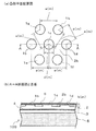
表1には、ゴムのなかでも比較的柔らかいとされる弾性率1MPaのシリコーンゴムからなる場合(例1〜3)、エンジニアリングプラスティクの代表であり、静電チャックでも一般に使用される弾性率1GPaのポリイミドからなる場合(例4、5)、及びゴムの中でも比較的硬いとされる弾性率10MPaの場合について、それぞれ弾性吸着層が備える凸部の例を示す。また、図1(a)は、この表1における凸部の配置関係を示す平面説明図である。この図1(a)では、直径d(m)の凸部1を一辺の長さがa(m)の正三角形の各頂点に配置している様子を示しており、そのうちのひとつ凸部1cを中心として、凸部1bから時計回り方向に凸部1g、凸部1h、凸部1d、凸部1f、及び凸部1eが配置されている。これらの凸部1は、静電チャック100における一部を示しているものであり、このような関係を有した配置状態で、凸部1が静電チャック100の基板吸着面を形成するように全面に分布する。また、図1(a)におけるA−A断面方向から見た静電チャック100の様子を図1(b)に示す。静電チャック100は、例えばアルミニウム金属で形成されたベース(金属基盤)5を有し、その上に下部絶縁層3と弾性吸着層2が積層されており、これらの間に吸着電極(内部電極)4を備えている。このうち、弾性吸着層2は、吸着電極4の上面側を電気的に絶縁する上部絶縁層を兼ねており、弾性吸着層2は、高さh(m)の凸部1を複数備えて、基板6を支持して基板吸着面を形成する。また、この弾性吸着層2における隣接した凸部1の間には、基板6とは接触しない上面2bを有する。Hereinafter, the present invention will be described in more detail with reference to the drawings.
Table 1 shows that, when rubber is made of silicone rubber having a modulus of elasticity of 1 MPa, which is considered to be relatively soft (Examples 1 to 3), it is a representative of engineering plastics and has a modulus of elasticity of 1 GPa that is also commonly used in electrostatic chucks. Examples of protrusions provided in the elastic adsorption layer are shown for the cases of polyimides (Examples 4 and 5) and the case of an elastic modulus of 10 MPa, which is relatively hard among rubbers. FIG. 1A is an explanatory plan view showing the arrangement relationship of convex portions in Table 1. FIG. FIG. 1A shows a state in which the
これらの例において、弾性吸着層2が直径298mmの基板吸着面を形成し、直径300mm、全体的平坦度Whが1μmのシリコン半導体基板を吸着力F=4900Pa(≒50gf/cm2)で吸着すると、先ず、例1では、比較的大きな凸部の直径dを有し(21mm)、その高さhも比較的高く(60μm)、凸部1の収縮量はδ=(h/nA)・(F/E)=1.02×10−6(m)であり、シリコン半導体基板の全体的平坦度Wh(m)と同等の値を得ることができ、尚且つ、基板吸着面における単位面積あたりの凸部頂面の総面積の割合ξが28.7(%)であることから、基板の冷却が極めて良好に行うことができる。また、例2では、例1に比べて凸部の高さhが低く、直径dも小さいが、凸部1の間隔aを狭めることで、例1と同等の収縮量δ=1.01μmを得ているものの、ξ=12.1%であって例1の半分であることから、基板の冷却能力は例1に比べて劣ることが予想される。例3では、凸部の直径dは例2と同じであり、その高さhを低くして、かつ、間隔aを更に小さくした場合であり、δは例2のおよそ半分になるが、ξは例2に比べて約20%向上する。一方、例4は、凸部の材料をポリイミドとした場合であり、凸部の高さh、直径d、間隔aは例1と同じであるが、δは弾性率に反比例して小さくなるため0.001μm程度と極めて小さな値になってしまう。そのため、凸部の柔軟性はほとんど期待できない。例5では、凸部の材料は例4と同じであるが、δは比較的大きな値が得られるものの、ξは極端に低下して0.1(%)となってしまい、基板との接触による熱伝導は期待できない。また、例6では、凸部の各寸法や配置を最適化してδ=0.532μmを得ているが、ξは6.4(%)にとどまる。In these examples, the

以下、実施例に基づき、本発明をより具体的に説明するが、本発明は、これらの内容に限定されるものではない。 EXAMPLES Hereinafter, although this invention is demonstrated more concretely based on an Example, this invention is not limited to these content.
[実施例1]
厚み100μm、300mm×300mmの薄膜シリコーンシート(サンシンエンタープライズ株式会社製、マイクロシリコーンシートの片面梨子地タイプ、型番NμKSA-100-50)を用意し、直径298mmの円形に切りだして、後述のようにして弾性吸着層2とした。また、厚さ50μmのポリイミドシートの片面に厚さ9μmの銅箔が積層された銅張積層板(宇部興産株式会社製、銅張積層板「ユピセル(登録商標)N」)を用いて、銅箔面にマスキングをして腐食性エッチング液にて半月型パターン(直径294mmの半円状)を有する双極型(電極間隔2mm)の吸着電極4を形成し、直径298mmのポリイミドシートを下部絶縁層3とした。そして、図2に示すように、銅張積層板の銅箔面側に、厚さ10μmのエポキシ系ボンディングシート(図示せず)を介して、シリコーンシートの梨子地面が表側になるよう接着した。一体に貼り合わされたシートは、内部に直径6mmの冷却水の水路7を有して、板厚15mm、直径298mmのアルミニウム製ベース5に対して、前述のエポキシ系ボンディングシートを介して貼着し、シリコーンシートの梨子地面が表側、すなわち基板吸着面となるようにした。[Example 1]
Prepare a thin film silicone sheet with a thickness of 100μm and 300mm x 300mm (manufactured by Sanshin Enterprise Co., Ltd., one-sided pear surface type of micro silicone sheet, model number NμKSA-100-50). Thus, an
次いで、上記マイクロシリコーンシートの梨子地面に、ステンレス製の所定のマスクを介して、空気式ブラストで粒径数μmのシリコン粒子を一定時間均一に照射して所定の上面2bを得た。すなわち、表1の例1に示したように、高さh=60μm、直径d=21mm、隣接する凸部の間隔a=37.3mmであり、梨子地面を頂面とする凸部1を形成して、基板吸着面に単位面積1m2当たりn=830個の凸部1を備える弾性吸着層2を得た。更に、吸着電極4を外部の電源10に接続するため、吸着電極4から電位供給線9を絶縁スリーブ8を通して外部に取り出し、実施例1に係る静電チャック101を完成させた。Next, silicon particles having a particle diameter of several μm were uniformly irradiated for a certain period of time by a pneumatic blast through a predetermined stainless steel mask on the pear ground of the microsilicon sheet to obtain a predetermined
上記で得た静電チャック101が、基板6を吸着力F=4900Paで吸着・保持したときに、弾性吸着層2における凸部1がどの程度接触するかを確認するため、以下のような試験を行った。直径300mm、厚み10mm、及び全体的平坦度Whが1μmの透明パイレックス(登録商標)ガラス板を凸部1の頂面からなる基板吸着面に載置し、平面の台座を有するプレス機により加圧した。この際、ガラス板の自重と加えた圧力とが単位面積あたり合計4900Paになるように管理した。先ず、加圧した状態で、透明パイレックス(登録商標)ガラス板を通して、目視により凸部1の接触状態を確認したところ、全ての凸部1がその頂面で接触していることが確認された。ちなみに、全ての凸部1がガラス板に接触している場合と、そうでない場合とを比べると、光の干渉縞の様子が異なるため、目視により両方の状態を判別することができる。また、別の試験方法として、ガラス板と静電チャック101の基板吸着面との間に感圧紙を挟み込み、上記と同様にしてプレス機により加圧したところ、全ての凸部1の箇所で感圧紙は反応しており、全ての凸部1がその頂面で接触していることが確認された。更に、比較実験として、ガラス板の自重と加えた圧力との合計を1/2とした、単位面積あたり合計2450Paの条件で同じ実験を行ったところ、全ての凸部1のうちの3分の2がガラス板にその頂面で接触することが確認された。In order to confirm how much the
[実施例2]
厚さ25μmのポリイミドシートに、表面が梨子地に処理された厚さ100μmのシリコーンシートが張り合わされた複合シート11、厚さ13μmのアクリルエポキシボンディングシート12、及び、厚さ12μmの電解銅箔13(古河サーキットフォイル(株)製)を、それぞれ直径298mmの円形に切り出して、プレス成型にて3MPa、170℃の条件で積層化した。[Example 2]
Composite sheet 11 in which a polyimide sheet with a thickness of 25 μm and a silicone sheet with a thickness of 100 μm whose surface is processed into a pear surface are pasted together, an acrylic
上記で積層化したプレス体の片面側の銅箔を双極電極とするために、その中心を対称軸として、10分割された隣り合う扇形形状の電極(隣接する電極間距離3mm)をエッチング処理により形成した。次いで、直径298mmに切り出した上記と同じ厚さ13μmのアクリルエポキシボンディングシート12を介して、上記でエッチングして得られた電極面を覆うように、厚さ50μmのポリイミドシート14(東レ・デュポン(株)製、カプトンフイルム型式200H)を重ね合わせ、上記と同じ条件により、プレス成型して一体に積層させた。
In order to use the copper foil on one side of the pressed body laminated as above as a bipolar electrode, etching is performed on adjacent fan-shaped electrodes (
次いで、厚さ55μmのカプトン片面粘着テープ(オカモト株式会社 1030E)を、上記で得られた積層体の梨子地面の全面に接着させ、更に、電極に端子を接合するため、ポリイミドシート14で覆われた電極面を上側に向けてホットプレート上に載せ、加熱しながら銅製の端子を半田付けした。
Next, a 55 μm thick Kapton single-sided adhesive tape (Okamoto Corporation 1030E) was adhered to the entire surface of the pear ground of the laminate obtained above, and further covered with a
次いで、上記で用いたものと同じカプトン片面粘着テープに、直径23mmの開口部の中心が一辺の長さが35mmの正三角形の各頂点に配置されるように複数の孔をあけてパターンマスクとし、これをアルミナポーラス真空チャック上に配置し、このパターンマスク上に、上記で得られた積層体の粘着テープ側を対向させるようにして載せて、1Paになるように真空に吸引した。これにより、パターンマスクの孔径と厚みに対応した凹凸が形成され、後述するように、最後にカプトン片面粘着テープを剥がした後には、梨子地面を有したシリコーンシートを頂面として、表2に示したような凸部が形成される。 Next, in the same Kapton single-sided adhesive tape as used above, a plurality of holes are formed so that the center of the opening with a diameter of 23 mm is arranged at each vertex of a regular triangle with a side length of 35 mm to form a pattern mask. This was placed on an alumina porous vacuum chuck, placed on the pattern mask so that the adhesive tape side of the laminate obtained above was opposed, and sucked to a vacuum of 1 Pa. As a result, irregularities corresponding to the hole diameter and thickness of the pattern mask are formed, and as will be described later, after the Kapton single-sided adhesive tape is finally peeled off, the silicone sheet having a pear ground is shown in Table 2 as the top surface. Convex portions are formed.
アルミナポーラス真空チャックで吸引した状態のまま、銅製の端子を取り付けた側のポリイミドシート面に、シリコーン接着剤15(モメンティブ・パフォーマンス・マテリアルズ・ジャパン合同会社、型式TSE3331)を厚さ150μmとなるように塗布した後、板厚16mm及び直径298mmであって内部に冷却水の水路を有したアルミ製のベース16を載せ、真空チャックを吸引しているポンプの電源を切り、脱泡チャンバー内で1時間脱泡させ、その後ホットプレート上で全体を140℃に加熱し、数時間かけてシリコーン接着剤を硬化させた。その後、一体化されたものを真空チャックから離脱させて清掃し、梨子地面を有したシリコーンシートを覆うカプトン片面粘着テープを剥がすことで、図3に示すような凸部1を備えた実施例2に係る静電チャック(No.1)を完成させた。
While being sucked with an alumina porous vacuum chuck, silicone adhesive 15 (Momentive Performance Materials Japan GK, Model TSE3331) is 150 μm thick on the polyimide sheet surface on which the copper terminals are attached. After coating, an
また、この実施例で得られた静電チャックの変形例として、上記表1に記した例3における凸部を形成するようにした以外は上記と同様にして、本発明の実施例に係る静電チャック(No.2)を得た。 Further, as a modified example of the electrostatic chuck obtained in this embodiment, the static chuck according to the embodiment of the present invention is the same as described above except that the convex portion in Example 3 described in Table 1 is formed. An electric chuck (No. 2) was obtained.
上記で得られたNo.1及びNo.2の静電チャックについて、それぞれイオン注入装置に搭載して、供給電圧±750Vでφ300mmのシリコンウエハを吸着・保持しながら、このシリコンウエハに対して、平均イオンビームパワー450W、注入量1×10¹⁵個/cm2の条件でイオン注入を行った。この際、アルミ製ベースの水路には2L/minの条件で冷却水を通水するようにした。そして、イオン注入時のウエハ表面温度をサーモラベルで計測したところ、No.1の静電チャックで吸着・保持した場合は、温度上昇を48℃未満に抑えることができ、No.2の静電チャックでは、温度上昇を89℃未満に抑えることができた。更には、No.1の静電チャックを用いた試験では、イオンビームパワーを600Wに増大させたときでも、上記と同じ注入量においても温度上昇は60℃未満という結果が得られた。これはガス冷却を伴う従来の静電チャックに匹敵する性能であるといえる。No. obtained above. 1 and no. Each of the
1:凸部
2:弾性吸着層
2b:弾性吸着層の凸部以外の上面
3:下部絶縁層
4:吸着電極
5:ベース
6:基板
7:水路
8:絶縁スリーブ
9:電位供給線
10:電源
11:複合シート
12:ボンディングシート
13:電解銅箔
14:ポリイミドシート
15:シリコーン接着剤
16:ベース
100、101:静電チャック1: Convex part 2: Elastic adsorption layer
2b: Upper surface other than the convex portion of the elastic adsorption layer 3: Lower insulating layer 4: Adsorption electrode 5: Base 6: Substrate 7: Water channel 8: Insulation sleeve 9: Potential supply line
10: Power supply
11: Composite sheet
12: Bonding sheet
13: Electrolytic copper foil
14: Polyimide sheet
15: Silicone adhesive
16: Base
100, 101: Electrostatic chuck
Claims (7)
弾性吸着層における凸部の高さをh、基板吸着面における単位面積当たりの凸部の数をn、凸部における頂面の面積をA、凸部を形成する弾性材料の弾性率をEとして、全体的平坦度がWhの基板を吸着力Fで吸着・保持したときに、吸着力Fが働く方向に凸部が収縮する量δが、以下の関係式(1)を満足するように弾性吸着層を形成し、かつ、基板吸着面における単位面積あたりの凸部頂面の総面積の割合ξを10%以上にすることを特徴とする静電チャックの製造方法。
5Wh≧δ≧0.5Wh、ここでδ=(h/nA)・(F/E) ・・・(1)
〔但し、各値の単位は、それぞれ括弧内に示したものである;Wh(m)、h(m)、n(個/m2)、A(m2)、E(Pa)、F(Pa)、δ(m)。〕An electrostatic chuck manufacturing method in which an elastic adsorption layer having a plurality of convex portions made of an elastic material is used as a substrate adsorption surface, and the substrate is adsorbed and held via the elastic adsorption layer,
The height of the convex portion in the elastic adsorption layer is h, the number of convex portions per unit area on the substrate adsorption surface is n, the area of the top surface of the convex portion is A, and the elastic modulus of the elastic material forming the convex portion is E. when the overall flatness and the substrate W h adsorbed and held by the suction force F, as the convex portions in the direction in which acts the suction force F is the amount of shrinkage δ satisfies the following equation (1) A method for manufacturing an electrostatic chuck, comprising: forming an elastic adsorption layer, and setting the ratio ξ of the total area of the convex top surfaces per unit area on the substrate adsorption surface to 10% or more.
5 W h ≧ δ ≧ 0.5 W h , where δ = (h / nA) · (F / E) (1)
[However, the unit of each value is shown in parentheses; W h (m), h (m), n (pieces / m 2 ), A (m 2 ), E (Pa), F (Pa), δ (m). ]
Priority Applications (1)
| Application Number | Priority Date | Filing Date | Title |
|---|---|---|---|
| JP2010533896A JP5458323B2 (en) | 2008-10-15 | 2009-10-13 | Electrostatic chuck and manufacturing method thereof |
Applications Claiming Priority (4)
| Application Number | Priority Date | Filing Date | Title |
|---|---|---|---|
| JP2008289260 | 2008-10-15 | ||
| JP2008289260 | 2008-10-15 | ||
| PCT/JP2009/067734 WO2010044398A1 (en) | 2008-10-15 | 2009-10-13 | Electrostatic chuck, and method for manufacturing the chuck |
| JP2010533896A JP5458323B2 (en) | 2008-10-15 | 2009-10-13 | Electrostatic chuck and manufacturing method thereof |
Publications (2)
| Publication Number | Publication Date |
|---|---|
| JPWO2010044398A1 JPWO2010044398A1 (en) | 2012-03-15 |
| JP5458323B2 true JP5458323B2 (en) | 2014-04-02 |
Family
ID=42106561
Family Applications (1)
| Application Number | Title | Priority Date | Filing Date |
|---|---|---|---|
| JP2010533896A Active JP5458323B2 (en) | 2008-10-15 | 2009-10-13 | Electrostatic chuck and manufacturing method thereof |
Country Status (6)
| Country | Link |
|---|---|
| JP (1) | JP5458323B2 (en) |
| KR (1) | KR101559947B1 (en) |
| CN (1) | CN102187446B (en) |
| HK (1) | HK1158368A1 (en) |
| TW (1) | TWI467691B (en) |
| WO (1) | WO2010044398A1 (en) |
Families Citing this family (52)
| Publication number | Priority date | Publication date | Assignee | Title |
|---|---|---|---|---|
| CN102738293B (en) * | 2011-04-01 | 2014-12-17 | 北京北方微电子基地设备工艺研究中心有限责任公司 | Execution apparatus and manipulator |
| JP5505667B2 (en) | 2011-09-30 | 2014-05-28 | Toto株式会社 | AC drive electrostatic chuck |
| US8349116B1 (en) | 2011-11-18 | 2013-01-08 | LuxVue Technology Corporation | Micro device transfer head heater assembly and method of transferring a micro device |
| US8646505B2 (en) * | 2011-11-18 | 2014-02-11 | LuxVue Technology Corporation | Micro device transfer head |
| US8518204B2 (en) | 2011-11-18 | 2013-08-27 | LuxVue Technology Corporation | Method of fabricating and transferring a micro device and an array of micro devices utilizing an intermediate electrically conductive bonding layer |
| US8809875B2 (en) | 2011-11-18 | 2014-08-19 | LuxVue Technology Corporation | Micro light emitting diode |
| US8573469B2 (en) | 2011-11-18 | 2013-11-05 | LuxVue Technology Corporation | Method of forming a micro LED structure and array of micro LED structures with an electrically insulating layer |
| US9773750B2 (en) | 2012-02-09 | 2017-09-26 | Apple Inc. | Method of transferring and bonding an array of micro devices |
| US9548332B2 (en) | 2012-04-27 | 2017-01-17 | Apple Inc. | Method of forming a micro LED device with self-aligned metallization stack |
| US9105492B2 (en) | 2012-05-08 | 2015-08-11 | LuxVue Technology Corporation | Compliant micro device transfer head |
| US8415768B1 (en) | 2012-07-06 | 2013-04-09 | LuxVue Technology Corporation | Compliant monopolar micro device transfer head with silicon electrode |
| US8791530B2 (en) | 2012-09-06 | 2014-07-29 | LuxVue Technology Corporation | Compliant micro device transfer head with integrated electrode leads |
| US9162880B2 (en) | 2012-09-07 | 2015-10-20 | LuxVue Technology Corporation | Mass transfer tool |
| US9558721B2 (en) | 2012-10-15 | 2017-01-31 | Apple Inc. | Content-based adaptive refresh schemes for low-power displays |
| JP2014090038A (en) * | 2012-10-30 | 2014-05-15 | Kyocera Corp | Suction member |
| TWI514463B (en) * | 2012-11-30 | 2015-12-21 | Global Material Science Co Ltd | Method for manufacturing emboss surface of electric static chuck of dry etch apparatus |
| US9236815B2 (en) | 2012-12-10 | 2016-01-12 | LuxVue Technology Corporation | Compliant micro device transfer head array with metal electrodes |
| CN103904012B (en) * | 2012-12-28 | 2017-06-27 | 上海微电子装备有限公司 | A kind of vacuum cup of TSV silicon chips |
| US9217541B2 (en) | 2013-05-14 | 2015-12-22 | LuxVue Technology Corporation | Stabilization structure including shear release posts |
| US9484504B2 (en) | 2013-05-14 | 2016-11-01 | Apple Inc. | Micro LED with wavelength conversion layer |
| US9136161B2 (en) | 2013-06-04 | 2015-09-15 | LuxVue Technology Corporation | Micro pick up array with compliant contact |
| US8987765B2 (en) | 2013-06-17 | 2015-03-24 | LuxVue Technology Corporation | Reflective bank structure and method for integrating a light emitting device |
| US9111464B2 (en) | 2013-06-18 | 2015-08-18 | LuxVue Technology Corporation | LED display with wavelength conversion layer |
| US8928021B1 (en) | 2013-06-18 | 2015-01-06 | LuxVue Technology Corporation | LED light pipe |
| US9035279B2 (en) | 2013-07-08 | 2015-05-19 | LuxVue Technology Corporation | Micro device with stabilization post |
| US9296111B2 (en) | 2013-07-22 | 2016-03-29 | LuxVue Technology Corporation | Micro pick up array alignment encoder |
| US9087764B2 (en) | 2013-07-26 | 2015-07-21 | LuxVue Technology Corporation | Adhesive wafer bonding with controlled thickness variation |
| US9153548B2 (en) | 2013-09-16 | 2015-10-06 | Lux Vue Technology Corporation | Adhesive wafer bonding with sacrificial spacers for controlled thickness variation |
| US9367094B2 (en) | 2013-12-17 | 2016-06-14 | Apple Inc. | Display module and system applications |
| US9768345B2 (en) | 2013-12-20 | 2017-09-19 | Apple Inc. | LED with current injection confinement trench |
| US9450147B2 (en) | 2013-12-27 | 2016-09-20 | Apple Inc. | LED with internally confined current injection area |
| US9542638B2 (en) | 2014-02-18 | 2017-01-10 | Apple Inc. | RFID tag and micro chip integration design |
| US9583533B2 (en) | 2014-03-13 | 2017-02-28 | Apple Inc. | LED device with embedded nanowire LEDs |
| US9522468B2 (en) | 2014-05-08 | 2016-12-20 | Apple Inc. | Mass transfer tool manipulator assembly with remote center of compliance |
| US9318475B2 (en) | 2014-05-15 | 2016-04-19 | LuxVue Technology Corporation | Flexible display and method of formation with sacrificial release layer |
| US9741286B2 (en) | 2014-06-03 | 2017-08-22 | Apple Inc. | Interactive display panel with emitting and sensing diodes |
| US9624100B2 (en) | 2014-06-12 | 2017-04-18 | Apple Inc. | Micro pick up array pivot mount with integrated strain sensing elements |
| US9425151B2 (en) | 2014-06-17 | 2016-08-23 | Apple Inc. | Compliant electrostatic transfer head with spring support layer |
| US9570002B2 (en) | 2014-06-17 | 2017-02-14 | Apple Inc. | Interactive display panel with IR diodes |
| CN104209190A (en) * | 2014-08-30 | 2014-12-17 | 常州市群星印刷有限公司 | Air purifier |
| US9705432B2 (en) | 2014-09-30 | 2017-07-11 | Apple Inc. | Micro pick up array pivot mount design for strain amplification |
| US9828244B2 (en) | 2014-09-30 | 2017-11-28 | Apple Inc. | Compliant electrostatic transfer head with defined cavity |
| US9478583B2 (en) | 2014-12-08 | 2016-10-25 | Apple Inc. | Wearable display having an array of LEDs on a conformable silicon substrate |
| KR102206687B1 (en) * | 2017-06-26 | 2021-01-22 | 니뽄 도쿠슈 도교 가부시키가이샤 | Substrate holding member |
| JP6435481B1 (en) * | 2017-09-04 | 2018-12-12 | 株式会社プロセス・ラボ・ミクロン | Work suction jig and work suction device |
| CN110246797A (en) * | 2018-03-08 | 2019-09-17 | 弘塑科技股份有限公司 | Wafer mounting apparatus, wafer fixed pedestal and wafer vacuum sucker |
| TWI642138B (en) * | 2018-03-08 | 2018-11-21 | 弘塑科技股份有限公司 | Wafer fixing device, wafer fixing base and wafer vacuum chuck |
| KR102614668B1 (en) * | 2018-03-29 | 2023-12-19 | 가부시키가이샤 크리에이티브 테크놀러지 | suction pad |
| KR102093991B1 (en) * | 2018-08-31 | 2020-04-23 | 이지스코 주식회사 | Elastomer rubber diaphragm type electro static chuck and fabrication method for the same |
| JP7278193B2 (en) * | 2018-12-07 | 2023-05-19 | キヤノントッキ株式会社 | Deposition equipment |
| JP7183223B2 (en) * | 2020-08-28 | 2022-12-05 | 株式会社Screenホールディングス | SUBSTRATE PROCESSING APPARATUS AND SUBSTRATE PROCESSING METHOD |
| CN114056933B (en) * | 2021-12-17 | 2023-10-20 | 广东海拓创新精密设备科技有限公司 | High molecular weight modified siliconized polyurethane rubber physical adhesion sucking disc |
Family Cites Families (8)
| Publication number | Priority date | Publication date | Assignee | Title |
|---|---|---|---|---|
| JPS503100B1 (en) * | 1970-08-18 | 1975-01-31 | ||
| JPS5050980U (en) * | 1973-09-06 | 1975-05-17 | ||
| JPS60259428A (en) * | 1984-06-06 | 1985-12-21 | Toppan Printing Co Ltd | Manufacture of vinylon shape film |
| US5548470A (en) * | 1994-07-19 | 1996-08-20 | International Business Machines Corporation | Characterization, modeling, and design of an electrostatic chuck with improved wafer temperature uniformity |
| JPH10335439A (en) * | 1997-06-04 | 1998-12-18 | Shin Etsu Chem Co Ltd | Electrostatic chuck |
| JP4046424B2 (en) * | 1998-11-09 | 2008-02-13 | 株式会社アルバック | Substrate mounting apparatus and vacuum processing apparatus |
| TWI420579B (en) * | 2005-07-12 | 2013-12-21 | Creative Tech Corp | And a foreign matter removing method for a substrate |
| JP5059450B2 (en) | 2007-03-06 | 2012-10-24 | 東京エレクトロン株式会社 | Substrate mounting table and substrate processing apparatus |
-
2009
- 2009-10-12 TW TW98134496A patent/TWI467691B/en active
- 2009-10-13 JP JP2010533896A patent/JP5458323B2/en active Active
- 2009-10-13 KR KR1020117009769A patent/KR101559947B1/en active IP Right Grant
- 2009-10-13 CN CN200980141296.6A patent/CN102187446B/en not_active Expired - Fee Related
- 2009-10-13 WO PCT/JP2009/067734 patent/WO2010044398A1/en active Application Filing
-
2011
- 2011-11-23 HK HK11112707.6A patent/HK1158368A1/en not_active IP Right Cessation
Also Published As
| Publication number | Publication date |
|---|---|
| WO2010044398A1 (en) | 2010-04-22 |
| TW201026582A (en) | 2010-07-16 |
| KR20110084888A (en) | 2011-07-26 |
| KR101559947B1 (en) | 2015-10-13 |
| JPWO2010044398A1 (en) | 2012-03-15 |
| HK1158368A1 (en) | 2012-07-13 |
| CN102187446B (en) | 2013-07-24 |
| CN102187446A (en) | 2011-09-14 |
| TWI467691B (en) | 2015-01-01 |
Similar Documents
| Publication | Publication Date | Title |
|---|---|---|
| JP5458323B2 (en) | Electrostatic chuck and manufacturing method thereof | |
| JP5283699B2 (en) | Bipolar electrostatic chuck | |
| US7881036B2 (en) | Electrode sheet for electrostatic chuck, and electrostatic chuck | |
| EP1180793A2 (en) | Electrostatic chuck and manufacturing method thereof | |
| KR100976320B1 (en) | Electrostatic chuck and electrode sheet for electrostatic chuck | |
| KR20140007362A (en) | Work heating device and work treatment device | |
| WO2017130827A1 (en) | Electrostatic chuck device | |
| JPWO2008108146A1 (en) | Electrostatic chuck | |
| JP2008282875A (en) | Electrostatic chuck and method of manufacturing electrostatic chuck | |
| JP2009200393A (en) | Electrostatic chuck and method of manufacturing the same | |
| KR102127883B1 (en) | Electrostatic chuck with photo-patternable soft protrusion contact surface | |
| WO2012026421A1 (en) | Electrostatic chuck apparatus and method for manufacturing same | |
| KR101302886B1 (en) | Substrate mounting stage, method for forming resin protrudent layer to surface of substrate mounting stage, and resin protrudent layer transfering member | |
| JP2009141003A (en) | Electrostatic chuck | |
| JP5343802B2 (en) | Electrostatic chuck device | |
| JP3979694B2 (en) | Electrostatic chuck device and manufacturing method thereof | |
| JP4308564B2 (en) | Plasma processing apparatus and plasma processing tray | |
| JP6642170B2 (en) | Electrostatic chuck device and manufacturing method thereof | |
| JP2007005434A (en) | Electrostatic zipper device and electrode sheet therefor | |
| JP5795272B2 (en) | Method for manufacturing ceramic element | |
| US20220084866A1 (en) | Electrostatic chuck and substrate fixing device | |
| TWI813840B (en) | Electrostatic chuck device | |
| JP2006049357A (en) | Electrostatic chuck and equipment mounting it | |
| JP2023183628A (en) | Substrate fixing device and method for manufacturing substrate fixing device | |
| JP4529352B2 (en) | Laminated wafer for semiconductor manufacturing equipment |
Legal Events
| Date | Code | Title | Description |
|---|---|---|---|
| A621 | Written request for application examination |
Free format text: JAPANESE INTERMEDIATE CODE: A621 Effective date: 20120706 |
|
| A131 | Notification of reasons for refusal |
Free format text: JAPANESE INTERMEDIATE CODE: A131 Effective date: 20130625 |
|
| TRDD | Decision of grant or rejection written | ||
| A01 | Written decision to grant a patent or to grant a registration (utility model) |
Free format text: JAPANESE INTERMEDIATE CODE: A01 Effective date: 20131203 |
|
| A61 | First payment of annual fees (during grant procedure) |
Free format text: JAPANESE INTERMEDIATE CODE: A61 Effective date: 20131220 |
|
| R150 | Certificate of patent or registration of utility model |
Free format text: JAPANESE INTERMEDIATE CODE: R150 Ref document number: 5458323 Country of ref document: JP Free format text: JAPANESE INTERMEDIATE CODE: R150 |
|
| S531 | Written request for registration of change of domicile |
Free format text: JAPANESE INTERMEDIATE CODE: R313531 |
|
| R350 | Written notification of registration of transfer |
Free format text: JAPANESE INTERMEDIATE CODE: R350 |
|
| R250 | Receipt of annual fees |
Free format text: JAPANESE INTERMEDIATE CODE: R250 |
|
| R250 | Receipt of annual fees |
Free format text: JAPANESE INTERMEDIATE CODE: R250 |
|
| R250 | Receipt of annual fees |
Free format text: JAPANESE INTERMEDIATE CODE: R250 |
|
| R250 | Receipt of annual fees |
Free format text: JAPANESE INTERMEDIATE CODE: R250 |
|
| R250 | Receipt of annual fees |
Free format text: JAPANESE INTERMEDIATE CODE: R250 |
|
| R250 | Receipt of annual fees |
Free format text: JAPANESE INTERMEDIATE CODE: R250 |
|
| R250 | Receipt of annual fees |
Free format text: JAPANESE INTERMEDIATE CODE: R250 |
|
| R250 | Receipt of annual fees |
Free format text: JAPANESE INTERMEDIATE CODE: R250 |