JP4308564B2 - Plasma processing apparatus and plasma processing tray - Google Patents
Plasma processing apparatus and plasma processing tray Download PDFInfo
- Publication number
- JP4308564B2 JP4308564B2 JP2003104066A JP2003104066A JP4308564B2 JP 4308564 B2 JP4308564 B2 JP 4308564B2 JP 2003104066 A JP2003104066 A JP 2003104066A JP 2003104066 A JP2003104066 A JP 2003104066A JP 4308564 B2 JP4308564 B2 JP 4308564B2
- Authority
- JP
- Japan
- Prior art keywords
- substrate
- adhesive sheet
- tray
- plasma processing
- vacuum chamber
- Prior art date
- Legal status (The legal status is an assumption and is not a legal conclusion. Google has not performed a legal analysis and makes no representation as to the accuracy of the status listed.)
- Expired - Fee Related
Links
Images

Landscapes
- Plasma Technology (AREA)
Description
【0001】
【発明の属する技術分野】
本発明は、電子デバイスやマイクロマシン(MEMS:Micro Electromechanical Systems)、実装基板などの製造に利用されるプラズマ処理装置及びプラズマ処理用トレーに関するものである。
【0002】
【従来の技術】
一般的な平行平板型プラズマ処理装置の一例を図19に示す。
【0003】
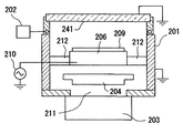
図19において、真空容器201内にガス供給装置202より所定のガスを導入しつつ排気装置としてのポンプ203で排気を行い、調圧弁204により真空容器201内を所定の圧力に保ちながら、基板電極用高周波電源210により13.56MHzの高周波電力を、基板電極206に印加すると、真空容器201内にプラズマが発生し、基板電極206上に載置された基板209に対してエッチング、堆積、表面改質等のプラズマ処理を行うことができる。ターボ分子ポンプ203及び排気口211は、基板電極206の直下に配置されており、また、調圧弁204は、基板電極206の直下で、かつ、ターボ分子ポンプ203の直上に位置する昇降弁である。基板電極206は、4本の支柱212により、真空容器201に固定されている。また、基板電極206に対向して、対向電極241が設けられている。
【0004】
他のプラズマ処理装置に、コイルに高周波電力を印加することによって真空容器内にプラズマを発生させる高周波誘導方式のプラズマ処理装置がある。この方式のプラズマ処理装置は、真空容器内に高周波磁界を発生させ、その高周波磁界によって真空容器内に誘導電界を発生させて電子の加速を行い、プラズマを発生させるもので、平行平板型プラズマよりも高い密度のプラズマを発生させることができる。
【0005】
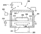
その構成の一例を図20に示す。図20において、真空容器201内に、ガス供給装置202から所定のガスを導入しつつ、排気装置としてのターボ分子ポンプ203により排気を行い、調圧弁204により真空容器201内を所定の圧力に保ちながら、コイル用高周波電源205により13.56MHzの高周波電力を基板電極206に対向した誘電板207に沿って設けられたコイル208に供給することにより、真空容器201内に誘導結合型プラズマが発生し、基板電極206上に載置された基板209に対してプラズマ処理を行うことができる。
【0006】
また、基板電極206に高周波電力を供給するための基板電極用高周波電源210が設けられており、基板209に到達するイオンエネルギーを制御することができるようになっている。ターボ分子ポンプ203及び排気口211は、基板電極206の直下に配置されており、また、調圧弁204は、基板電極206の直下で、かつ、ターボ分子ポンプ203の直上に位置する昇降弁である。基板電極206は、4本の支柱212により、真空容器201に固定されている。
【0007】
基板電極の表面材質については、これまでも様々な材料が用いられてきた。アルミニウムやステンレスなどの金属はもとより、特許文献1に記載されているように、基板電極の表面の一部分だけを絶縁層(硬質アルマイト)で覆い、その絶縁層のみが基板と接触するよう構成する例、特許文献2に記載されているように、基板電極の基板と接触する部分を誘電体膜(塩化ビニル、テフロン(四フッ化エチレン樹脂(Polytetrafluoroethylene)成形品の米国デュポン社の商品名で登録商標)、又はポリイミド)で覆う例、特許文献3に記載されているように、塩化ビニル、テフロン、又はポリイミドの少なくとも一つからなる誘電体膜で基板電極の基板と接触する部分を覆いつつ、基板電極の自己バイアス電圧をモニタして、誘電体膜の損傷を検出する例、などがある。このように、基板と基板電極間に誘電体層を設けると、チャージアップダメージを低減できるという効果がある。
【0008】
或いは、基板電極の表面をセラミック層で覆い、セラミック層に埋め込まれた直流電極に直流電圧を印加して、基板を静電気力で基板電極表面に吸着させたり、基板をクランプリングで基板電極に押し付けたりすることによって、基板と基板電極の熱伝導を改善する方法もある。さらに、基板と基板電極の間に熱媒体となる気体(ヘリウムなど)を供給して、基板と基板電極の熱伝導を高める方法もある。
【0009】
【特許文献1】
特許第2758755号
【特許文献2】
特開平2−155230号公報
【特許文献3】
特許第3010683号
【0010】
【発明が解決しようとする課題】
しかしながら、前述するような従来の方式では、薄くて柔らかい基板(例えば、樹脂シートなど)を処理しようとしても、プラズマ照射によって基板の温度が上昇してしまうという問題点があった。
【0011】
これは、基板の熱容量が小さいことに加え、真空中では基板と基板電極の熱交換が不十分になることに起因している。仮に静電気力で基板を基板電極表面に吸着させようとしても、誘電体製基板は直流電流がごくわずかしか流れないため、吸着させることができず、また仮に、基板をクランプリングで基板電極に押し付けた上で、基板と基板電極の間に熱媒体となる気体を供給しても、基板が薄くて柔らかいために大きく変形し、処理の均一性が損なわれるばかりか、基板と基板電極の間にできた空間で異常放電が発生する場合があり、実用に耐えない。
【0012】
また、従来の方式において、基板が大型で、薄くて固く、かつ割れやすいもの(シリコン、ガラス、又は、セラミックスなど)である場合に、基板と基板電極の間に熱媒体となる気体を供給すると、基板が薄いために大きく変形し、基板が割れてしまうこともある。とくに、基板の厚さが1mm以下で、面積が0.1m2以上である場合、このような問題が生じる場合がある。
【0013】
本発明の目的は、上記従来の問題点に鑑み、基板の温度制御性を向上することができるプラズマ処理装置及びプラズマ処理用トレーを提供することである。
【0014】
【課題を解決するための手段】
上記目的を達成するために、本発明は以下のように構成する。
【0015】
請求項1の本発明によれば、基板又は上記基板上の膜を処理するプラズマ処理に用いられる、プラズマ処理用トレーであって、
上記基板が載置される面の表面に配置された粘着性シートを備え、
上記基板が載置される面と反対側の表面に配置された別の粘着性シートを備え、
上記基板が載置される面の表面に、所定間隔をあけて配置された複数の樹脂テープを備えるとともに、
上記基板が載置される面の表面と上記複数の樹脂テープとの上に上記粘着性シートが配置されて、上記粘着性シートの粘着力により、上記複数の樹脂テープと上記基板が載置される面の表面との上に固定された状態で、各樹脂テープの両側に各樹脂テープと上記粘着性シートとの間に大略帯状空隙が形成されているとともに、上記粘着性シートの上面に上記複数の樹脂テープにより凹凸面が形成され、かつ、上記大略帯状空隙の両端は上記粘着性シートの周囲に開放されているプラズマ処理用トレーを提供する。
請求項2の本発明によれば、凸形の形状を有する請求項1に記載のプラズマ処理用トレーを提供する。
請求項3の本発明によれば、排気穴を備えて、上記排気穴を通じて上記基板との間の気体を排気して、上記基板を上記粘着性シートに接触可能である請求項1に記載のプラズマ処理用トレーを提供する。
請求項4の本発明によれば、上記粘着性シートは、誘電体の上記基板と接触可能である請求項1〜3のいずれか1つに記載のプラズマ処理用トレーを提供する。
請求項5の本発明によれば、基板を、表面に上記粘着性シートが設けられかつ請求項1〜4のいずれか1つに記載された上記プラズマ処理用トレー上に載置する基板載置ステーションと、
真空室と、
上記真空室内にガスを供給するためのガス供給装置と、
上記真空室内を排気するための排気装置と、
上記真空室内を所定の圧力に制御するための調圧弁と、
上記真空室内に上記トレーを載置するための基板電極と、
上記基板電極又はプラズマ源に高周波電力を供給することのできる高周波電源とを備えるプラズマ処理装置を提供する。
本発明の第1態様によれば、真空室内にガスを供給しつつ上記真空室内を排気し、上記真空室内を所定の圧力に制御しながら、上記真空室内にプラズマを発生させて、上記真空室内の基板電極に載置した基板又は基板上の膜を処理するプラズマ処理方法であって、
上記基板電極と上記基板との間に配置された粘着性シートを介して上記基板と上記基板電極との熱交換を行いつつ上記基板又は上記基板上の膜を処理するプラズマ処理方法を提供する。
【0016】
本発明の第2態様によれば、真空室内にガスを供給しつつ上記真空室内を排気し、上記真空室内を所定の圧力に制御しながら、上記真空室内にプラズマを発生させ、上記真空室内の基板電極に載置したトレー上の基板又は基板上の膜を処理するプラズマ処理方法であって、
上記トレーと上記基板との間に配置された粘着性シートを介して上記トレーと上記基板電極との熱交換を行いつつ上記基板又は上記基板上の膜を処理するプラズマ処理方法を提供する。
【0017】
本発明の第3態様によれば、上記基板電極と上記トレーとの間に配置された粘着性シートを介して上記基板電極と上記トレーとの熱交換を行いつつ上記基板又は上記基板上の膜を処理する第2の態様に記載のプラズマ処理方法を提供する。
【0018】
本発明の第4態様によれば、真空室内に基板を搬送し、
上記基板を上記真空室内の基板電極に向かって凸形に変形させながら保持し、上記凸形に変形した基板の中央付近を上記基板電極の表面に設けられた粘着性シートに接触させ、
上記基板の片面のほぼ全域を上記基板電極の表面に設けられた上記粘着性シートに接触させ、
上記真空室内にガスを供給しつつ上記真空室内を排気し、上記真空室内を所定の圧力に制御しながら、上記真空室内にプラズマを発生させて、上記基板又は上記基板上の膜を処理することを含むプラズマ処理方法を提供する。
【0019】
本発明の第5態様によれば、真空室内に基板を搬送し、
上記真空室内の凸形の基板電極の上方に上記基板を保持し、
上記基板の中央付近を上記基板電極の表面に設けられた粘着性シートに接触させ、
上記基板の外縁部を上記基板電極に押し付けて、上記基板の片面のほぼ全域を上記基板電極の表面に設けられた上記粘着性シートに接触させ、
上記真空室内にガスを供給しつつ上記真空室内を排気し、上記真空室内を所定の圧力に制御しながら、上記真空室内にプラズマを発生させて、上記基板又は上記基板上の膜を処理することを含むプラズマ処理方法を提供する。
【0020】
本発明の第6態様によれば、基板の片面のほぼ全域をトレーの表面に設けられた粘着性シートに接触させ、
上記真空室内に上記トレーを搬送し、
上記真空室内の基板電極の上方に上記トレーを保持し、
上記トレーを上記基板電極上に載置し、
上記真空室内にガスを供給しつつ上記真空室内を排気し、上記真空室内を所定の圧力に制御しながら、上記真空室内にプラズマを発生させて、上記基板又は上記基板上の膜を処理することを含むプラズマ処理方法を提供する。
【0021】
本発明の第7態様によれば、上記粘着性シートの熱伝導率が、0.1W/m・K以上である第1,2,4,5,6のいずれか1つの態様に記載のプラズマ処理方法を提供する。
【0022】
本発明の第8態様によれば、上記粘着性シートのアスカーCが、80以下である第1,2,4,5,6のいずれか1つの態様に記載のプラズマ処理方法を提供する。
【0023】
本発明の第9態様によれば、上記粘着性シートの硬さが、50〜60である第1,2,4,5,6のいずれか1つの態様に記載のプラズマ処理方法を提供する。
【0024】
本発明の第10態様によれば、上記粘着性シートの厚さが、0.05〜0.5mmである第1,2,4,5,6のいずれか1つの態様に記載のプラズマ処理方法を提供する。
【0025】
本発明の第11態様によれば、上記基板がガラス又はセラミックスである第1,2,4,5,6のいずれか1つの態様に記載のプラズマ処理方法を提供する。
【0026】
本発明の第12態様によれば、上記基板が樹脂シートである第1,2,4,5,6のいずれか1つの態様に記載のプラズマ処理方法を提供する。
【0027】
本発明の第13態様によれば、上記基板の厚さが0.001〜1mmである、第1,2,4,5,6のいずれか1つの態様に記載のプラズマ処理方法を提供する。
【0028】
本発明の第14態様によれば、上記基板の厚さが0.001〜0.5mmである、第1,2,4,5,6のいずれか1つの態様に記載のプラズマ処理方法を提供する。
【0029】
本発明の第15態様によれば、上記基板のヤング率をE(Pa)、上記基板のポアソン比をν、上記基板の代表長さをa(m)、上記基板の厚さをh(m)としたとき、600×(1−ν2)a4/(256×Eh3)>0.005(m)である第1,2,4,5,6のいずれか1つの態様に記載のプラズマ処理方法を提供する。
【0030】
本発明の第16態様によれば、真空室と、
上記真空室内にガスを供給するためのガス供給装置と、
上記真空室内を排気するための排気装置と、
上記真空室内を所定の圧力に制御するための調圧弁と、
上記真空室内に基板を載置するための基板電極と、
上記基板電極又はプラズマ源に高周波電力を供給することのできる高周波電源と、
上記基板電極の表面に配置されて上記基板を載置させる粘着性シートとを備えるプラズマ処理装置を提供する。
【0031】
本発明の第17態様によれば、基板を、表面に粘着性シートが設けられたトレー上に載置するための基板載置ステーションと、
真空室と、
上記真空室内にガスを供給するためのガス供給装置と、
上記真空室内を排気するための排気装置と、
上記真空室内を所定の圧力に制御するための調圧弁と、
上記真空室内に上記トレーを載置するための基板電極と、
上記基板電極又はプラズマ源に高周波電力を供給することのできる高周波電源とを備えるプラズマ処理装置を提供する。
【0032】
本発明の第18態様によれば、上記粘着性シートの熱伝導率が、0.1W/m・K以上である第16又は17の態様に記載のプラズマ処理装置を提供する。
【0033】
本発明の第19態様によれば、上記粘着性シートのアスカーCが、80以下である第16又は17の態様に記載のプラズマ処理装置を提供する。
【0034】
本発明の第20態様によれば、上記粘着性シートの硬さが、50〜60である第16又は17の態様に記載のプラズマ処理装置を提供する。
【0035】
本発明の第21態様によれば、上記粘着性シートの厚さが、0.05〜0.5mmである第16又は17の態様に記載のプラズマ処理装置を提供する。
【0036】
本発明の第22態様によれば、基板又は上記基板上の膜を処理するプラズマ処理に用いられる、プラズマ処理用トレーであって、
上記基板が載置される面の表面に配置された粘着性シートを備えるプラズマ処理用トレーを提供する。
【0037】
本発明の第23態様によれば、上記基板が載置される面と反対側の表面に配置された別の粘着性シートを備える第22の態様に記載のプラズマ処理用トレーを提供する。
【0038】
本発明の第24態様によれば、上記粘着性シートの熱伝導率が、0.1W/m・K以上である第22の態様に記載のプラズマ処理用トレーを提供する。
【0039】
本発明の第25態様によれば、上記粘着性シートのアスカーCが、80以下である第22の態様に記載のプラズマ処理用トレーを提供する。
【0040】
本発明の第26態様によれば、上記粘着性シートの硬さが、50〜60である第22の態様に記載のプラズマ処理用トレーを提供する。
【0041】
本発明の第27態様によれば、上記粘着性シートの厚さが、0.05〜0.5mmである第22の態様に記載のプラズマ処理用トレーを提供する。
【0042】
【発明の実施の形態】
本発明の記述を続ける前に、添付図面において同じ部品については同じ参照符号を付している。
【0043】
以下に、本発明にかかる実施の形態を図面に基づいて詳細に説明する。
【0044】
(第1の実施形態)
以下、本発明の第1実施形態について、図1〜図4(C)及び図34,図35を参照して説明する。
【0045】
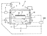
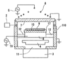
図1に、本発明の第1実施形態において用いたプラズマ処理装置の断面図を示す。
【0046】
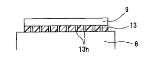
図1において、真空室の一例としての真空容器1内に、ガス供給装置2から所定のガスを導入しつつ、排気装置としてのターボ分子ポンプ3により排気を行い、調圧弁4により真空容器1内を所定の圧力に保ちながら、コイル用高周波電源5により13.56MHzの高周波電力を基板電極6に対向した誘電板7に沿って設けられたコイル(プラズマ源の一例)8に供給することにより、真空容器1内に誘導結合型プラズマが発生し、基板電極6上に載置された基板9に対してプラズマ処理を行うことができる。
【0047】
この明細書及び請求の範囲において、基板9とは、薄くて柔らかい基板を意味し、例えば、樹脂シート(例えばポリイミドのシート)、紙などに回路が形成されたものを意味する。
【0048】
また、基板電極6に高周波電力を供給するための基板電極用高周波電源10が設けられており、基板9に到達するイオンエネルギーを制御することができるようになっている。ターボ分子ポンプ3及び排気口11は、基板電極6の直下に配置されており、また、調圧弁4は、基板電極6の直下で、かつ、ターボ分子ポンプ3の直上に位置する昇降弁である。基板電極6は、4本の支柱12により、真空容器1に固定されている。上記ガス供給装置2、コイル用高周波電源5、基板電極用高周波電源10、ターボ分子ポンプ3、及び、調圧弁4のそれぞれの動作は、制御装置1000により制御される。なお、制御装置1000については、他の実施形態でも同様であるため、代表的に図1にのみ図示し、他の実施形態では原則として図示を省略する。
【0049】
基板電極6と基板9との間に粘着性シート13が設けられ、粘着性シート13を介して基板9と基板電極6との熱交換を行いつつ処理することができるようになっている。
【0050】
粘着性シート13の一例として、シリコンゴムフィルムを用いている。粘着性シート13は、シートの材料自体に自己粘着性(self−tack)を有するものである。粘着性シート13の大きさは、基板9よりも若干小さく、例えば、外縁より少なくとも1mm程度以上小さくすることにより、プラズマ処理中にプラズマによる劣化を防止できるようにすることが好ましい。この粘着性シート13の熱伝導率は0.2W/m・K、アスカーCは60、硬さは55、厚さは0.2mmである。
【0051】
なお、アスカーC(ASKER C)とは、樹脂の柔らかさの指標であって、アスカーCが60とは、アスカーC硬度計で測定した値が60と言うことを示しており、針入度,稠度試験とは逆に数字が大きいほど硬い材料を意味する。
アスカーCは、日本ゴム協会標準規格(SRIS)の規格0101のスプリング式アスカーC型を意味し、日本工業規格(JIS)のK6301−1995(加硫ゴム物理試験方法)に以下の測定方法が規定されている。
【0052】
スプリング式硬さ試験(A形及びC形)
試験片は、原則としてA形では厚さ12mm以上のものを用い、12mm未満のものは積み重ねて、なるべく12mm以上とする。C形では厚さ6mm以上のものを用い、6mm未満のものは積み重ねて、なるべく6mm以上とする。
【0053】
また、試験片の測定面は、平滑でない場合は平滑になるように研磨する。測定面は、試験機の加圧面が、少なくともその測定面内に入るような大きさが必要である。
【0054】
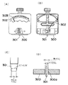
試験機は、一例として図29(A)及び(B)のようなスプリング式硬さ試験機のA形又はC形を用いる。この試験機は、試験片表面に加圧面300を接触させたとき、加圧面300の中心の穴300aからばね圧力によって突き出ている押針301(図29(C)参照)がゴム面によって押し戻される距離を硬さとして目盛303に示すようになっている。加圧面300は、押針301に垂直な平面で、その中心に図29(D)のような押針301を通す穴があり、その径は10mm以上でなければならない。目盛303及び押針301の動きとばねの力との関係を示す基準線(図30(A)及び(B)参照)の許容差は、A形では±0.0785N{±8gf}、C形では±0.196N{±20gf}とする。また、押針301の動きと指針302の動きの間には遊びがあってはならない。押針301の材質は磨耗しにくく、かつ、さびにくいもので、その形状及び寸法は、図29(C)〜(D)のとおりとする。押針301は加圧面300の穴300aの中心に正しく取り付け、目盛0のときの針先は、加圧面300から2.540 −0.05mmだけ突き出ていて、目盛100のときの針先面は、加圧面300と同一平面上になければならない。目盛は0〜100の間を等間隔に分割する。
【0055】
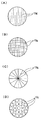
また、粘着性シート13には、粘着性シート13と基板9との間に隙間若しくは気泡が生じるのを効果的に防止するために、図21又は図22に示すように、互いに連通して気泡が抜けやすくなっている、貫通穴13h又は溝13gを形成するようにしてもよい。また、溝13gの配置の仕方としては、図23(A)に示すように互いに平行に直線的に配置したり、図23(B)に示すように格子状に配置したり、図23(C)に示すように放射状に配置したり、図23(D)に示すように多数の凸部13jの間に溝を配置してもよい。
【0056】
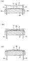
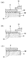
図2(A)〜(C)は、表面に、フォトレジストでパターニングされた厚さ300nmのシリコン酸化膜を有する、厚さh=0.4mm=0.0004mのポリイミド樹脂製基板9を基板電極6に載置する工程を示す。なお、基板のヤング率Eは3GPa、ポアソン比νは0.3、基板は円形で、その直径aは0.15mである。
【0057】
まず、真空容器1の開閉ゲート22から真空容器1内に基板9を搬送アーム23により搬送した後、基板9を複数個のリフトピン14(支持部材の一例)で保持する(図2(A))。このとき、基板電極6に設けられた貫通穴6a内を昇降する複数個のリフトピン14が、基板電極6の外縁付近に設けられているため、基板9は基板電極6に向かって凸形に変形する。リフトピン14は、基板9の中心に対して点対称に複数個(例えば、図34に示されるように4個、又は、図35に示されるように3個)配置されている。複数個のリフトピン14の下端は、駆動リング100に固定され、駆動リング100は、制御装置1000の動作制御の元に、駆動装置の一例としてのエアシリンダ101などにより昇降駆動されるようになっている。これに限らず、リフトピン14毎に、又は、所定数のリフトピン14毎に昇降駆動するエアシリンダ101などの駆動装置を設けて、リフトピン14毎に又は所定数のリフトピン14毎に昇降可能とすることにより、複数本のリフトピン14を1本ずつ又は所定本数ずつ順に上昇させることにより、基板電極6又は粘着性シート13から簡単に取り外しできるようにしてもよい。
【0058】
次に、制御装置1000の動作制御の元にエアシリンダ101の駆動により駆動リング100が下降させられて、複数個のリフトピン14を同時的に徐々に降下させ、まず最初に、基板9の中央付近を基板電極6の表面に設けられた粘着性シート13に接触させる(図2(B))。
【0059】
さらに、リフトピン14を降下させることで、基板9の周囲部分も粘着性シート13に接触させて、基板9の片面のほぼ全域を基板電極6の表面に設けられた粘着性シート13に接触させることができる(図2(C))。
【0060】
このような搬送手順を用いることにより、基板9と粘着性シート13の間に、気体が残留する隙間ができないようにすることができる。
【0061】
基板9を基板電極6に載置した後、基板電極6の温度を30℃に保ちつつ、真空容器1内にCF4ガスを5sccm、Arガスを45sccm供給し、真空容器1内の圧力を3Paに保ちながら、コイル8に500W、基板電極6に200Wの高周波電力をそれぞれ印加する条件で、基板9上のシリコン酸化膜をエッチング処理したところ、100nm/minのエッチング速度でエッチングを行うことができた。処理時間は、オーバーエッチング時間を含めて200秒である。その結果、フォトレジストの焼けは発生せず、良好なエッチング処理が行えた。なお、同一の条件で基板9の温度を測定したところ、エッチング終了間際の基板9の温度は57℃であった。比較のために、従来の方式(粘着性シートの無い構成)で同様の条件にてエッチング処理を行ったところ、フォトレジストの焼けが生じ、エッチングに失敗した。また、同一の条件で基板9の温度を測定したところ、エッチング終了間際の基板9の温度は195℃であった。
【0062】
このように、従来例と比べて基板9の温度が大幅に低下したのは、粘着性シート13を介して基板9と基板電極6との熱交換を行いつつ処理することができたためである。
【0063】
処理後、粘着性シート13から基板9を取り外すときは、上記搬送手順とは逆に、まず、制御装置1000の動作制御の元に、エアシリンダ101により駆動リング100が上昇されて、複数個のリフトピン14を同時的に徐々に上昇させて、粘着性シート13から基板9を剥がすように取り外したのち、搬送アーム23に基板9を移し換えて、真空容器1内から搬出させる。
【0064】
このとき、例えば、複数個のリフトピン14の長さを異ならせることにより、同時的に粘着性シート13から基板9を取り外すのではなく、長いリフトピン14と短いリフトピン14とで基板9を粘着性シート13の表面に対して傾斜させて支持させるようにすれば、基板9の周囲を同時的に粘着性シート13の表面から取り外すのではなく、長いリフトピン14で基板9の周囲の一部の部分をまず粘着性シート13の表面から取り外したのち、短いリフトピン14で基板9の周囲の残りの部分を粘着性シート13の表面から取り外すことにより、より円滑に基板9を粘着性シート13の表面から取り外すことができるようにしてもよい。このような動作を行なわせるために、先に述べたように各リフトピン14を別々に上昇できるようにしてもよい。
【0065】
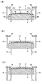
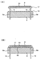
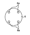
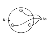
基板9を基板電極6に載置する工程の別の例を図3(A)〜(C)に示す。まず、真空容器1内に基板9を搬送した後、基板9を保持する(図3(A))。このとき、中央部が頂部となるように上向きに湾曲して突出した凸部6bを有する基板電極6Aに設けられた貫通穴6a内を昇降するリフトピン14が、基板電極6Aの外縁付近に設けられているため、基板9は基板電極6Aに向かって凸形に変形する。
【0066】
次に、リフトピン14を徐々に降下させ、基板9の中央付近を、図の左右方向の中央部が湾曲して突出した凸部6bの表面を有する凸形の基板電極6Aの凸部6bの表面に設けられた粘着性シート13に接触させる(図3(B))。さらに、リフトピン14を降下させることで、基板9の片面のほぼ全域を基板電極6Aの凸部6b表面に設けられた粘着性シート13に接触させることができる(図3(C))。この例では、例えば曲率が1/100〜1/10の凸形の基板電極6Aを用いているので、変形しにくい基板9を扱う場合にも、確実に基板9の中央付近から先に粘着性シート13に接触させることができ、基板9と粘着性シート13の間に隙間ができる可能性を低下させることができる。曲率が1/100より小さい場合には、隙間減少効果が少ない一方、曲率が1/10を超える場合には基板9に形成される回路パターンに損傷が生じやすくなるため、上記範囲が好ましい。
【0067】
基板9を基板電極6に載置する工程のさらに別の例を図4(A)〜(C)に示す。まず、真空容器1内に基板9を搬送した後、基板9を保持する(図4(A))。この例では、基板9が変形しにくい材質であるため、図2(A)〜(C)や図3(A)〜(C)の場合とは違って、基板9が基板電極6に向かって凸形に変形する度合いが大幅に少ない。
【0068】
次に、リフトピン14を降下させ、基板9の中央付近を凸形の基板電極6の表面に設けられた粘着性シート13に接触させる(図4(B))。
【0069】
次に、リング昇降棒15を用いてクランプリング16を降下させ、基板9の外縁部を基板電極6に押し付けることにより、基板9の片面のほぼ全域を基板電極6の表面に設けられた粘着性シート13に接触させることができる(図4(C))。この例では、凸形の基板電極6を用いているので、変形しにくい基板9を扱う場合にも、確実に基板9の中央付近から先に粘着性シート13に接触させることができ、基板9と粘着性シート13の間に隙間ができる可能性を低下させることができる。
【0070】
クランプリング16の基板9に接触する下面には、部分的に、押え付け補助部材として、図4(A)に点線で示すように、粘着材16dを備えて、クランプリング16により基板9を基板電極6に押え付けるとき、基板9との間に粘着力を発生させて基板9を基板電極6に対して、ずれなく、より確実に押え付ける一方、クランプリング16を上昇させるとき、粘着材16dの粘着力により基板9を少しだけ持ち上げるようにして、基板9を基板電極6から取り外ししやすくするようにしてもよい。一方、クランプリング16に部分的に若しくは全面的にかつクランプリング16の図4(A)に点線で示す部分に、別の押え付け補助部材として、粘着力が無く、単なる凹凸のある凹凸部材を配置して、クランプリング16により基板9を基板電極6に押え付けるときに基板9との間に摩擦力を発生させて、基板9を基板電極6に対して、ずれなく、より確実に押え付けることができるようにしてもよい。
【0071】
また、図24(A)及び(B)に示すように、基板電極6の表面に形成した凹部6dに対して隙間90を空けて粘着性シート13を配置し、クランプリング16により基板9とともに粘着性シート13が押圧されて、粘着性シート13が隙間90内に入り込むことにより、基板9と基板電極6との間に気泡などの隙間が形成されないようにしてもよい。また、図24(C)に示すように、特に、凹部6dを基板電極6の表面に形成することなく、クランプリング16により基板9とともに粘着性シート13が押圧されるとき粘着性シート13自身が圧縮されることにより、基板9と基板電極6との間に気泡などの隙間が形成されないようにしてもよい。
【0072】
(第2の実施形態)
本発明の第2実施形態について、図5〜図17(C)を参照して説明する。
【0073】
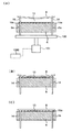
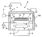
図5に、本発明の第2実施形態において用いたプラズマ処理装置の断面図を示す。
【0074】
図5において、真空容器1内に、ガス供給装置2から所定のガスを導入しつつ、排気装置としてのターボ分子ポンプ3により排気を行い、調圧弁4により真空容器1内を所定の圧力に保ちながら、コイル用高周波電源5により13.56MHzの高周波電力を基板電極6に対向した誘電板7に沿って設けられたコイル8に供給することにより、真空容器1内に誘導結合型プラズマが発生し、基板電極6上に載置された基板9に対してプラズマ処理を行うことができる。
【0075】
また、基板電極6に高周波電力を供給するための基板電極用高周波電源10が設けられており、基板9に到達するイオンエネルギーを制御することができるようになっている。ターボ分子ポンプ3及び排気口11は、基板電極6の直下に配置されており、また、調圧弁4は、基板電極6の直下で、かつ、ターボ分子ポンプ3の直上に位置する昇降弁である。基板電極6は、4本の支柱12により、真空容器1に固定されている。
【0076】
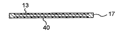
基板9は、トレー17に載置されており、トレー17と基板9との間に粘着性シート13が設けられ、粘着性シート13を介して基板9とトレー17との熱交換を行いつつ処理することができるようになっている。粘着性シート13として、シリコンゴムフィルムを用いた。この粘着性シート13の熱伝導率は0.2W/m・K、アスカーCは60、硬さは55、厚さは0.2mmである。
【0077】
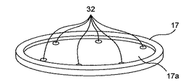
トレー17は、厚さ2〜5mmで、耐塩素ガス性を有しかつ酸化被膜が表面に形成された熱伝導性の良い材料が好ましく、例えば、アルミニウムの表面に酸化被膜としてアルマイト処理したものが好ましい。
【0078】
トレー17内に配置される粘着性シート13の収納用円形凹部17aは、粘着性シート13と大略同一の大きさとするか、又は、先に述べたように、図24(A),(B)に示すように、粘着性シート13よりも大きくして、基板9がクランプリング16で押え付けられるとき、粘着性シート13が径方向外向きにはみ出ることが可能なようにしてもよい。
【0079】
基板9、トレー17を基板電極6に載置した後、基板電極6の温度を30℃に保ちつつ、真空容器1内にCF4ガスを5sccm、Arガスを45sccm供給し、真空容器1内の圧力を3Paに保ちながら、コイル8に500W、基板電極6に200Wの高周波電力をそれぞれ印加する条件で、基板9上のシリコン酸化膜をエッチング処理したところ、100nm/minのエッチング速度でエッチングを行うことができた。
【0080】
処理時間は、オーバーエッチング時間を含めて200秒である。その結果、フォトレジストの焼けは発生せず、良好なエッチング処理が行えた。なお、同一の条件で基板9の温度を測定したところ、エッチング終了間際の基板9の温度は92℃であった。比較のために、従来の方式(粘着性シートの無い構成)で同様の条件にてエッチング処理を行ったところ、フォトレジストの焼けが生じ、エッチングに失敗した。また、同一の条件で基板9の温度を測定したところ、エッチング終了間際の基板9の温度は200℃であった。
【0081】
このように、従来例と比べて基板9の温度が大幅に低下したのは、粘着性シート13を介して基板9とトレー17との熱交換を行いつつ処理することができたためである。つまり、基板9のみの熱容量よりも、トレー17の熱容量がはるかに大きい(10倍以上)ため、プラズマ照射による温度上昇が低減したと考えることができる。トレー17を用いると、トレー17を用いない本発明の第1実施形態の構成よりも基板9の温度が高くなってしまっているが、トレー17を用いることで、基板9が真空中で搬送される際に位置ずれを起こす可能性が著しく低減する。すなわち、薄くかつ軽い基板9のみを搬送する場合には搬送中に搬送アームに対して基板が容易に位置ずれを起こしやすかったが、ある程度の重量がありかつ厚みのあるトレー17を用いることにより、搬送中に搬送アームに対して基板が位置ずれを起こしにくくなり、基板9の真空中の搬送を容易にできる効果がある。
【0082】
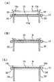
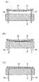
なお、図6に示すように、基板電極6とトレー17との間に粘着性シート18を設け、粘着性シート18を介して基板電極6とトレー17との熱交換を行いつつ処理することで、基板9の温度上昇をさらに抑えることが可能である。このような構成において、基板9を載置したトレー17を基板電極6に載置する工程を図7(A),(B)に示す。まず、真空容器1内に基板9を載置したトレー17を搬送した後、トレー17を保持する(図7(A))。
【0083】
次に、リフトピン14を徐々に降下させ、トレー17の片面のほぼ全域を基板電極6の表面に設けられた粘着性シート18に接触させる(図7(B))。トレー17と基板電極6の平面度及び平行度が十分あれば、トレー17と粘着性シート18の間に隙間ができないようにすることができる。
【0084】
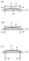
トレー17を基板電極6に載置する工程の別の例を図8(A)〜(C)に示す。まず、真空容器1内に基板9を載置したトレー17を搬送した後、トレー17を保持する(図8(A))。
【0085】
次に、リフトピン14を降下させ、トレー17を基板電極6の表面に設けられた粘着性シート18に接触させる(図8(B))。
【0086】
次に、リング昇降棒15を用いてクランプリング16を降下させ、トレー17の外縁部を基板電極6に押し付けることにより、トレー17の片面のほぼ全域を基板電極6の表面に設けられた粘着性シート18に接触させることができる(図8(C))。この例では、より確実に、トレー17と粘着性シート18の間に隙間ができないようにすることができる。
【0087】
なお、トレー17の外縁部を基板電極6に押し付ける代わりに、基板9の外縁部を基板電極6に押し付けてもよい。ただし、基板9が面に垂直な方向の力に弱い場合、トレー17の外縁部を基板電極6に押し付ける方が基板9に与える損傷が少ない点で好ましい。
【0088】
上記実施形態では、基板9を搬送して粘着性シート13に載置するようにしたが、図25(A)〜(C)に示すように、基板9の下面に予め粘着性シート13を取り外し可能にかつ気泡が無いように密着するように貼り付けた状態で、基板9と粘着性シート13とを一体的に搬送して複数個のリフトピン14で載置して基板電極6上に載置し粘着固定するようにしてもよい。この基板昇降時には、複数個のリフトピン14は、粘着性シート13を貫通して基板9を直接支持することにより、安定して基板9を昇降できるようにする。このように予め基板9の下面に粘着性シート13を貼り付けた状態で搬送すれば、基板電極6への配置時に、基板9の下面と粘着性シート13との間に気泡が入り込んで隙間ができることが効果的に防止できる。
【0089】
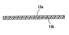
また、図26に示すように、粘着性シート13は1層のみから構成するものに限らず、2層より構成されるようにしてもよい。すなわち、粘着性シート13が、図26に示されるように、上側粘着性シート13aと下側粘着性シート13bとの2層から構成されるようにしてもよい。この場合、(上側粘着性シート13aの硬さ>下側粘着性シート13bの硬さ)のとき、上側粘着性シート13aの方が粘着性が低く、脱着性に富むので、電極やトレーの上面に粘着性シートを貼り付ける場合に適する。逆に、(上側粘着性シート13aの硬さ<下側粘着性シート13bの硬さ)のとき、下側粘着性シート13bの方が粘着性が低く、脱着性に富むので、トレーの下面や基板9に粘着性シートを貼り付ける場合に適する。
【0090】
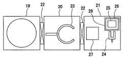
図9は、本発明の第2実施形態において用いたプラズマ処理装置の全体構成を示す平面図である。プラズマ処理を行うための反応チャンバ19(真空容器1を含む)、ロードロックチャンバ20、大気搬送部21の3つのユニットから成り、各ユニットは、開閉ゲートであるゲート弁22で仕切られている。ロードロックチャンバ20内には搬送アーム23が設けられ、大気搬送部21とロードロックチャンバ20間のトレー17の受け渡しと、反応チャンバ19とロードロックチャンバ20間のトレー17の受け渡しを行うことができる。大気アーム24は、基板カセット25又はトレーカセット26との間で、基板9又はトレー17を受け渡しするためのものである。
【0091】
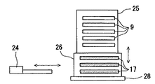
また、大気アームは、基板9を、表面に粘着性シート13が設けられたトレー17上に載置するための基板載置ステーション27との間で、基板9又はトレー17の受け渡しを行う。基板カセット25及びトレーカセット26は、カセット昇降台28の上に設けられる。大気アーム24が、基板カセット25又はトレーカセット26と、基板9又はトレー17を受け渡しするとき、大気アーム24が、図10に示すように、前後運動を行う一方で、カセット昇降台28が適切なタイミングで昇降するようになっている。
【0092】
図11(A)〜(E)は、トレー17に粘着性シート13を貼り付ける手順を示す。まず、トレー17と、両面が保護フィルム29及び30で覆われた粘着性シート13を用意する(図11(A))。
【0093】
次に、保護フィルム30の一部を剥がしてトレー17の粘着性シート配置用凹部17aの底面に接触させ、引き続いて保護フィルム30の一端を引っ張りながら、保護フィルム29の上からローラー31を回転させて、トレー17の粘着性シート配置用凹部17a内に粘着性シート13を貼り付けていく(図11(B)、(C))。
【0094】
次に、保護フィルム29を剥がす(図11(D))。
【0095】
このような手順で、基板9が載置される面の表面に粘着性シート13を備えたトレー17を得ることができる(図11(E))。
【0096】
基板9をトレー17に載置する工程において、基板9とトレー17の密着性を良くするために、トレー17Aが、図の左右方向の中央部が湾曲して突出した凸部17bの表面を有する凸形であることが好ましい場合がある。このような場合に、トレー17Aに粘着性シート13を貼り付ける手順を図12(A)〜(E)に示す。まず、凸形のトレー17Aと、両面が保護フィルム29及び30で覆われた粘着性シート13を用意する(図12(A))。
【0097】
次に、保護フィルム30の一部を剥がしてトレー17Aに接触させ、引き続いて保護フィルム30の一端を引っ張りながら、保護フィルム29の上からローラー31を回転させて、トレー17Aに粘着性シート13を貼り付けていく(図12(B)、(C))。
【0098】
次に、保護フィルム29を剥がす(図12(D))。このような手順で、基板9が載置される面の表面に粘着性シート13を備えた凸形のトレー17Aを得ることができる(図12(E))。
【0099】
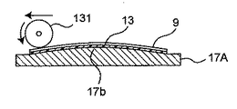
なお、図27に示すように、トレー17Aの粘着性シート13上に基板9を載置したのち、基板9上でローラー131を回転させて、基板9と粘着性シート13との間の隙間を無くすようにしてしてもよい。
【0100】
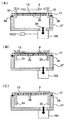
基板9をトレー17に載置する工程の例を図13及び図14(A)〜(C)に示す。
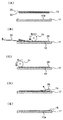
【0101】
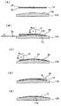
図13はトレー17の斜視図で、リフトピン33を昇降させるための貫通穴32が例えば粘着性シート配置用凹部17aの底面に設けられている。まず、基板載置ステーション27(図9参照)にトレー17及び基板9を搬送した後、基板9をトレー17の上方に保持する(図14(A))。このとき、トレー17に設けられた貫通穴32内を昇降するリフトピン33が、トレー17の外縁付近に設けられているため、基板9はトレー17に向かって凸形に変形する。次に、リフトピン33を徐々に降下させ、基板9の中央付近をトレー17の表面に設けられた粘着性シート13に接触させる(図14(B))。
【0102】
さらに、リフトピン33を降下させることで、基板9の片面のほぼ全域をトレー17の表面に設けられた粘着性シート13に接触させることができる(図14(C))。
【0103】
このような手順を用いることにより、基板9と粘着性シート13の間に隙間ができないように(言い換えれば、気泡が入り込まないように)することができる。
【0104】
基板9をトレー17Aに載置する工程の別の例を図15(A)〜(C)に示す。まず、基板載置ステーション27(図9参照)にトレー17A及び基板9を搬送した後、基板9をトレー17Aの上方に保持する(図15(A))。このとき、トレー17Aに設けられた貫通穴32内を昇降するリフトピン33が、トレー17Aの外縁付近に設けられているため、基板9はトレー17Aに向かって凸形に変形する。
【0105】
次に、リフトピン33を徐々に降下させ、基板9の中央付近を凸形のトレー17Aの表面に設けられた粘着性シート13に接触させる(図15(B))。
【0106】
さらに、リフトピン33を降下させることで、基板9の片面のほぼ全域をトレー17Aの表面に設けられた粘着性シート13に接触させることができる(図15(C))。この例では、凸形のトレー17Aを用いているので、変形しにくい基板9を扱う場合にも、確実に基板9の中央付近から先に粘着性シート13に接触させることができ、基板9と粘着性シート13の間に隙間ができる可能性を低下させることができる。
【0107】
基板9をトレー17Aに載置する工程のさらに別の例を図16(A)〜(C)に示す。基板載置ステーション27(図9参照)にトレー17A及び基板9を搬送した後、基板9をトレー17Aの上方に保持する(図16(A))。この例では、基板9が変形しにくい材質であるため、図14(A)〜(C)や図15(A)〜(C)の場合とは違って、基板9がトレー17Aに向かって凸形に変形する度合いが大幅に少ない。
【0108】
次に、リフトピン33を降下させ、基板9の中央付近を凸形のトレー17Aの表面に設けられた粘着性シート13に接触させる(図16(B))。
【0109】
次に、複数の治具昇降棒34を用いて、基板9の外縁部に当接可能な枠状又は棒状のクランプ治具35を降下させ、基板9の外縁部をトレー17Aに押し付けることにより、基板9の片面のほぼ全域をトレー17Aの表面に設けられた粘着性シート13に接触させることができる(図16(C))。
【0110】
この例では、凸形のトレー17Aを用いているので、変形しにくい基板9を扱う場合にも、確実に基板9の中央付近から先に粘着性シート13に接触させることができ、基板9と粘着性シート13の間に隙間ができる可能性を低下させることができる。なお、真空容器1内にトレー17Aを搬送する際、クランプ治具35で基板9の外縁部をトレー17Aに押し付けたまま、トレー17Aを搬送することが好ましい。
【0111】
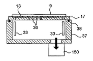
基板9をトレー17に載置する工程のさらに別の例を図17(A)〜(C)に示す。まず、基板載置ステーション27(図9参照)にトレー17及び基板9を搬送した後、基板9をトレー17の上方に保持する(図17(A))。この例では、トレー17に多数の排気穴36が設けられている。そして、基板9とトレー17との間の気体を排気装置150で排気しながらリフトピン33を降下させ、基板9の中央付近をトレー17の表面に設けられた粘着性シート13に接触させる(図17(B))。
【0112】
さらに、リフトピン33を降下させることで、基板9の片面のほぼ全域をトレー17の表面に設けられた粘着性シート13に接触させることができる(図17(C))。この例では、基板9とトレー17との間の気体を排気しながら工程を行うため、基板9と粘着性シート13の間に隙間ができる可能性が低く、また、基板9と粘着性シート13の間に気泡ができにくいという利点がある。
【0113】
なお、基板載置ステーション27(図9参照)が第2の真空容器内に設けられていてもよく、この場合も基板9と粘着性シート13の間に気泡ができにくいという利点がある。
【0114】
なお、図28に示すように、トレー17の中央部分にのみ排気穴36を設けることにより、基板9の中央部分のみを粘着性シート13に向けて吸着することにより、基板中央部分から周囲に向けて順に貼り付けられるようにして、隙間又は気泡をより効果的に除去できるようにしてもよい。
【0115】
以上述べた本発明の実施形態においては、本発明の適用範囲のうち、真空容器の形状、プラズマ源の方式及び配置等に関して様々なバリエーションのうちの一部を例示したに過ぎない。本発明の適用にあたり、ここで例示した以外にも様々なバリエーションが考えられることは、言うまでもない。
【0116】
また、ドライエッチングに適用する場合を例示したが、CVD、スパッタ等のプラズマ処理に適用可能であることは、言うまでもない。
【0117】
また、真空容器内の圧力が3Paである場合を例示したが、従来例において基板と基板電極、基板とトレー、又は、トレーと基板電極の熱交換が問題となるのは、概ね500Pa以下の圧力領域であるから、本発明はこのような圧力範囲において特に有効である。
【0118】
また、トレー上に載置された基板上の膜を処理する場合を例示したが、基板そのものを処理する場合にも適用できる。
【0119】
また、トレーの片面に粘着性シートが設けられている場合を例示したが、図18に示すように、トレーの両面に粘着性シートが設けられていてもよい。この場合、基板電極の表面に粘着性シートを設ける必要が無く、粘着性シートの張り替えが容易であるという利点がある。
【0120】
また、粘着性シートの熱伝導率が0.2W/m・Kである場合を例示したが、基板と基板電極、基板とトレー、又は、トレーと基板電極の熱交換を高めるためには、粘着性シートの熱伝導率が、0.1W/m・K以上であることが好ましい。
【0121】
また、粘着性シートのアスカーCが60である場合を例示したが、基板と基板電極、基板とトレー、又は、トレーと基板電極の熱交換を高めるためには、粘着性シートのアスカーCが、80以下であることが好ましい。アスカーCが80より大きいと、密着性が悪くなるため、熱交換能力が低下する。
【0122】
また、粘着性シートの硬さが55である場合を例示したが、基板と基板電極、基板とトレー、又は、トレーと基板電極の熱交換を高めるためには、粘着性シートの硬さが、50〜60であることが好ましい。粘着性シートの硬さが50より小さいと、粘着性シートが柔らかすぎて密着面に気泡が入りやすく、逆に、粘着性シートの硬さが60より大きいと、粘着性シートが硬すぎて密着度が悪くなってしまう。
【0123】
また、粘着性シートの厚さが0.2mmである場合を例示したが、基板と基板電極、基板とトレー、又は、トレーと基板電極の熱交換を高めるためには、粘着性シートの厚さが、0.05〜0.5mmであることが好ましい。粘着性シートの厚さが0.05mmより小さいと、粘着性シートの取扱いが困難となり、基板電極やトレーに粘着性シートを貼り付ける工程がうまく行えないとともに、粘着性シート自体のクッション性が不充分となり、平面度がでにくくなり冷却効率が悪化してしまう。逆に、粘着性シートの厚さが0.5mmより大きいと、熱抵抗が大きくなり、熱交換能力が低下する。
【0124】
また、基板がポリイミド樹脂製である場合を例示したが、本発明は様々な基板を用いる場合に適用可能である。導電性基板であれば、静電吸着によってある程度基板の温度を制御できる可能性があるので、本発明は、とくに、基板が誘電体である場合に有効である。そのような場合の例として、基板が、ガラス、セラミックス、樹脂シートなどである場合が考えられる。
【0125】
また、基板の厚さが0.4mmである場合を例示したが、本発明は、基板の厚さが、0.001〜1mmである場合にとくに有効で、さらに、基板の厚さが、0.001〜0.5mmである場合にとくに有効である。基板の厚さが0.001mm以下であると、基板の搬送が困難となる。逆に、基板の厚さが1mm以上であると、基板の熱容量が大きいため、処理中の基板温度変化は比較的小さくなる。高周波電力が小さい場合(例えば100W程度)には、基板の厚さが0.5mm〜1mmであっても、基板の熱容量が大きいため、処理中の基板温度変化は比較的小さくなる。あるいは、基板が大型で、薄くて固く、かつ割れやすいもの(シリコン、ガラス、セラミックスなど)である場合に、とくに、基板の厚さが1mm以下で、面積が0.1m2以上である場合には、従来例で述べたように熱媒体としての気体を用いることが困難であるから、本発明がとくに有効となる。
【0126】
また、基板の厚さhが0.0004m、ヤング率Eが3GPa、ポアソン比νが0.3、基板が円形で、その直径aが0.15mである場合を例示したが、本発明は、基板のヤング率をE(Pa)、基板のポアソン比をν、基板の代表長さをa(m)、基板の厚さをh(m)としたとき、600×(1−ν2)a4/(256×Eh3)>0.005(m)である場合にとくに有効なプラズマ処理方法である。すなわち、上述の関係式を満たすような基板を処理する場合に、とくに大きい効果を奏する。
【0127】
一般に、円板のヤング率をE(Pa)、ポアソン比をν、直径をa(m)、厚さをh(m)としたとき、円板の周辺を固定して円板に等分布荷重p(Pa)を作用させた場合の撓み量は、円板の中心において3×(1−ν2)pa4/(256×Eh3)(m)となる。基板の周辺をクランプリングなどで固定して、基板と基板電極の間に熱媒体となる気体を供給することによって基板の温度制御を行うには、通常200Pa以上の気体圧力が必要となることが知られている。
【0128】
つまり、600×(1−ν2)a4/(256×Eh3)>0.005なる式を満たすような基板とは、周辺を固定され、かつ、200Paの気体圧力がかかった際の撓みが0.005m(=5mm)以上となってしまうような基板を意味する。これほどの大きい変形を生じると、処理の均一性が損なわれるばかりか、基板と基板電極の間にできた空間で異常放電が発生する場合もあり、さらには、基板上に形成されたデバイスが応力によって破壊することもある。
【0129】
なお、ここでは円形の基板について説明したが、長方形などの他の形状においても、その代表長さa(たとえば長方形の対角線)をとれば、概ね600×(1−ν2)a4/(256×Eh3)>0.005なる式にて、本発明の適用効果の大きい範囲を定義づけることができる。逆に、上式を満たさない基板であれば、熱媒体としての気体を用いても変形しにくいため、本発明を適用するまでもなく、従来方法による処理が可能となる場合もある。
【0130】
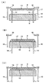
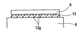
本発明の上記実施形態の他の変形例を図31から図33に示す。図31から図33において、複数の樹脂テープ130が所定間隔をあけて基板電極6の表面に配置され、複数の樹脂テープ130と基板電極6の表面との上に粘着性シート13Cが配置されて、粘着性シート13Cの粘着力により、複数の樹脂テープ130と基板電極6の表面との上に固定される。この状態で、各樹脂テープ130の両側に各樹脂テープ130と粘着性シート13Cとの間で大略帯状空隙132が形成されているとともに、粘着性シート13Cの上面にも、複数の樹脂テープ130による凹凸形状が、それらの段差が若干緩和されるものの転写されて、凹凸面が形成されている。
【0131】
図33に示されるように、粘着性シート13Cが配置される領域よりも、各樹脂テープ130の両端がはみ出るようになるため、各樹脂テープ130の両側に粘着性シート13Cとの間で形成された大略帯状空隙132のそれぞれの両端は、粘着性シート13Cで閉鎖されることなく、粘着性シート13Cの周囲に開放されている。この結果、基板電極6への粘着性シート貼付時に基板電極側の大略帯状の空隙132に溜まっている空気は、真空容器を排気する際に基板電極側の大略帯状の空隙132を通って排気され、気泡の膨張に起因した粘着シート13Cの変形は生じない。
【0132】
また、粘着性シート13Cの凹凸面である上面に基板9を載置して、粘着性シート13Cの粘着力により粘着性シート13Cに基板9を固定するとき、粘着性シート13Cの凹凸面と基板9の下面との間には、大略帯状の空隙131が形成されるが、各空隙131は、長手方向両端部で開放されている。よって、基板9を粘着性シート13Cに載置する際、基板側の各大略帯状空隙131に溜まっている空気は、真空容器を排気する際に基板側の大略帯状空隙131を通って排気され、気泡の膨張に起因した粘着シート13Cの変形は生じない。
【0133】
なお、基板電極6の上面に凹凸面を形成するには、上記したように複数の樹脂テープ130を用いず、基板電極6の表面そのものに溝を形成しておいてもよい。また、上記のような気泡の膨張を防止する手段は、トレーと基板の間、電極とトレーの間にも適用できることは言うまでもない。
【0134】
【発明の効果】
以上の説明から明らかなように、本発明の第1態様のプラズマ処理方法によれば、真空室内にガスを供給しつつ上記真空室内を排気し、上記真空室内を所定の圧力に制御しながら、上記真空室内にプラズマを発生させて、上記真空室内の基板電極に載置した基板又は基板上の膜を処理するプラズマ処理方法であって、上記基板電極と上記基板との間に配置された粘着性シートを介して上記基板と上記基板電極との熱交換を行いつつ上記基板又は上記基板上の膜を処理するため、基板の温度制御性を向上することができる。
【0135】
また、本発明の第2態様のプラズマ処理方法によれば、真空室内にガスを供給しつつ上記真空室内を排気し、上記真空室内を所定の圧力に制御しながら、上記真空室内にプラズマを発生させ、上記真空室内の基板電極に載置したトレー上の基板又は基板上の膜を処理するプラズマ処理方法であって、上記トレーと上記基板との間に配置された粘着性シートを介して上記トレーと上記基板電極との熱交換を行いつつ上記基板又は上記基板上の膜を処理するため、基板の温度制御性を向上することができる。
【0136】
また、本発明の第4態様のプラズマ処理方法によれば、真空室内に基板を搬送し、上記基板を上記真空室内の基板電極に向かって凸形に変形させながら保持し、上記凸形に変形した基板の中央付近を上記基板電極の表面に設けられた粘着性シートに接触させ、上記基板の片面のほぼ全域を上記基板電極の表面に設けられた上記粘着性シートに接触させ、上記真空室内にガスを供給しつつ上記真空室内を排気し、上記真空室内を所定の圧力に制御しながら、上記真空室内にプラズマを発生させて、上記基板又は上記基板上の膜を処理することを含むため、基板の温度制御性を向上することができる。
【0137】
また、本発明の第5態様のプラズマ処理方法によれば、真空室内に基板を搬送し、上記真空室内の凸形の基板電極の上方に上記基板を保持し、上記基板の中央付近を上記基板電極の表面に設けられた粘着性シートに接触させ、上記基板の外縁部を上記基板電極に押し付けて、上記基板の片面のほぼ全域を上記基板電極の表面に設けられた上記粘着性シートに接触させ、上記真空室内にガスを供給しつつ上記真空室内を排気し、上記真空室内を所定の圧力に制御しながら、上記真空室内にプラズマを発生させて、上記基板又は上記基板上の膜を処理することを含むため、基板の温度制御性を向上することができる。
【0138】
また、本発明の第6態様のプラズマ処理方法によれば、基板の片面のほぼ全域をトレーの表面に設けられた粘着性シートに接触させ、上記真空室内に上記トレーを搬送し、上記真空室内の基板電極の上方に上記トレーを保持し、上記トレーを上記基板電極上に載置し、上記真空室内にガスを供給しつつ上記真空室内を排気し、上記真空室内を所定の圧力に制御しながら、上記真空室内にプラズマを発生させて、上記基板又は上記基板上の膜を処理することを含むため、基板の温度制御性を向上することができる。
【0139】
また、本発明の第16態様のプラズマ処理装置によれば、真空室と、上記真空室内にガスを供給するためのガス供給装置と、上記真空室内を排気するための排気装置と、上記真空室内を所定の圧力に制御するための調圧弁と、上記真空室内に基板を載置するための基板電極と、上記基板電極又はプラズマ源に高周波電力を供給することのできる高周波電源と、上記基板電極の表面に配置されて上記基板を載置させる粘着性シートとを備えるため、基板の温度制御性を向上することができる。
【0140】
また、本発明の第17態様のプラズマ処理装置によれば、基板を、表面に粘着性シートが設けられたトレー上に載置するための基板載置ステーションと、真空室と、上記真空室内にガスを供給するためのガス供給装置と、上記真空室内を排気するための排気装置と、上記真空室内を所定の圧力に制御するための調圧弁と、上記真空室内に上記トレーを載置するための基板電極と、上記基板電極又はプラズマ源に高周波電力を供給することのできる高周波電源とを備えたため、基板の温度制御性を向上することができる。
【0141】
また、本発明の第22態様のプラズマ処理用トレーによれば、基板又は上記基板上の膜を処理するプラズマ処理に用いられる、プラズマ処理用トレーであって、上記基板が載置される面の表面に配置された粘着性シートを備えたため、基板の温度制御性を向上することができる。
【0142】
なお、上記様々な実施形態のうちの任意の実施形態を適宜組み合わせることにより、それぞれの有する効果を奏するようにすることができる。
【0143】
本発明は、添付図面を参照しながら好ましい実施形態に関連して充分に記載されているが、この技術の熟練した人々にとっては種々の変形や修正は明白である。そのような変形や修正は、添付した請求の範囲による本発明の範囲から外れない限りにおいて、その中に含まれると理解されるべきである。
【図面の簡単な説明】
【図1】 本発明の第1実施形態にかかるプラズマ処理方法で用いるプラズマ処理装置の構成を示す断面図である。
【図2】 (A),(B),(C)は、それぞれ、本発明の上記第1実施形態にかかる上記プラズマ処理方法における、基板を基板電極に載置する工程を示す断面図である。
【図3】 (A),(B),(C)は、本発明の上記第1実施形態にかかる上記プラズマ処理方法における、上記基板を上記基板電極に載置する工程を示す断面図である。
【図4】 (A),(B),(C)は、本発明の上記第1実施形態にかかる上記プラズマ処理方法における、上記基板を上記基板電極に載置する工程を示す断面図である。
【図5】 本発明の第2実施形態にかかるプラズマ処理方法で用いるプラズマ処理装置の構成を示す断面図である。
【図6】 本発明の第2実施形態にかかる上記プラズマ処理方法で用いる上記プラズマ処理装置の構成を示す断面図である。
【図7】 (A),(B)は、本発明の第2実施形態にかかる上記プラズマ処理方法における、トレーを基板電極に載置する工程を示す断面図である。
【図8】 (A),(B),(C)は、本発明の第2実施形態にかかる上記プラズマ処理方法における、上記トレーを上記基板電極に載置する工程を示す断面図である。
【図9】 本発明の第2実施形態にかかる上記プラズマ処理方法において用いる上記プラズマ処理装置の全体構成を示す平面図である。
【図10】 本発明の第2実施形態にかかる上記プラズマ処理方法における大気アームとカセットの動作を示す断面図である。
【図11】 (A),(B),(C),(D),(E)は、本発明の第2実施形態にかかる上記プラズマ処理方法において、トレーに粘着性シートを貼り付ける手順を示す断面図である。
【図12】 (A),(B),(C),(D),(E)は、本発明の第2実施形態にかかる上記プラズマ処理方法において、上記トレーに上記粘着性シートを貼り付ける手順を示す断面図である。
【図13】 本発明の第2実施形態にかかる上記プラズマ処理方法における上記トレーの斜視図である。
【図14】 (A),(B),(C)は、本発明の第2実施形態にかかる上記プラズマ処理方法における、基板をトレーに載置する工程を示す断面図である。
【図15】 (A),(B),(C)は、本発明の第2実施形態にかかる上記プラズマ処理方法における、上記基板を上記トレーに載置する工程を示す断面図である。
【図16】 (A),(B),(C)は、本発明の第2実施形態にかかる上記プラズマ処理方法における、上記基板を上記トレーに載置する工程を示す断面図である。
【図17】 (A),(B),(C)は、本発明の第2実施形態にかかる上記プラズマ処理方法における、上記基板を上記トレーに載置する工程を示す断面図である。
【図18】 本発明の一実施形態にかかるトレーの構成を示す断面図である。
【図19】 従来例で用いたプラズマ処理装置の構成を示す断面図である。
【図20】 従来例で用いたプラズマ処理装置の構成を示す断面図である。
【図21】 本発明の上記実施形態の変形例において、粘着性シートに貫通穴が設けられている場合の一部断面説明図である。
【図22】 本発明の上記実施形態の変形例において、粘着性シートに溝が設けられている場合の一部断面説明図である。
【図23】 (A),(B),(C),(D)は、それぞれ、本発明の上記実施形態の粘着性シートの様々な変形例の説明図である。
【図24】 (A),(B),(C)は、それぞれ、本発明の上記実施形態において基板電極の凹部に対して隙間を空けて粘着性シートを配置した状態を説明する説明図、クランプリングにより基板とともに粘着性シートが押圧されて隙間内に粘着性シートが入り込む状態を説明する説明図、基板電極の凹部に対して隙間無しで粘着性シートを配置した状態を説明する説明図である。
【図25】 (A),(B),(C)は、それぞれ、本発明の上記実施形態の変形例において、粘着性シートが基板と一緒に搬送される場合の説明図である。
【図26】 本発明の上記実施形態の変形例において、粘着性シートが2層より構成される場合の説明図である。
【図27】 本発明の上記実施形態の変形例において、トレーの粘着性シート上に基板を載置したのち、基板上でローラーを回転させる状態を説明する説明図である。
【図28】 本発明の上記実施形態の変形例において、トレーの中央部分にのみ排気穴を設ける場合を説明する説明図である。
【図29】 (A),(B),(C),(D)は、アスカーCを説明するためのスプリング式硬さ試験機のA形又はC形の正面図、裏蓋を取り外した状態の裏面図、押針の先端拡大図、押針と加圧面との関係を示す部分断面図である。
【図30】 (A),(B)は、目盛及び押針の動きとばねの力との関係を示す基準線を示すための、加圧面と押針先との距離と、ばねによって針先に加わる荷重と、目盛りとのグラフである。
【図31】 本発明の上記実施形態の他の変形例において、粘着性シートが複数の樹脂テープと基板電極とで形成された凹凸面に配置される場合の断面図である。
【図32】 図31の円形部分IIIの拡大図である。
【図33】 粘着性シートが凹凸面に配置される前の図31の場合の平面図である。
【図34】 本発明の上記第1実施形態にかかる上記プラズマ処理方法における、基板電極の別々の変形例の平面図である。
【図35】 本発明の上記第1実施形態にかかる上記プラズマ処理方法における、基板電極の別々の変形例の平面図である。
【符号の説明】
1…真空容器、2…ガス供給装置、3…ターボ分子ポンプ、4…調圧弁、5…コイル用高周波電源、6,6A…基板電極、6a…貫通穴、6b…凸部、6d…凹部、7…誘電板、8…コイル、9…基板、10…基板電極用高周波電源、11…排気口、12…支柱、13,13C…粘着性シート、13a…上側粘着性シート、13b…下側粘着性シート、13g…溝、13h…貫通穴、13j…凸部、14…リフトピン、15…リング昇降棒、17,17A…トレー、17a…収納用円形凹部、17b…凸部、18…粘着性シート、19…反応チャンバ、20…ロードロックチャンバ、21…大気搬送部、22…ゲート弁、23…搬送アーム、24…大気アーム、25…基板カセット、26…トレーカセット、27…基板載置ステーション、28…カセット昇降台、29,30…保護フィルム、31…ローラー、32…貫通穴、33…リフトピン、34…治具昇降棒、35…クランプ治具、36…排気穴、90…隙間、100…駆動リング、101…エアシリンダ、130…樹脂テープ、131…大略帯状の空隙、132…大略帯状空隙、150…排気装置、1000…制御装置。[0001]
BACKGROUND OF THE INVENTION
The present invention relates to plasma processing used for manufacturing electronic devices, micro machines (MEMS: Micro Electromechanical Systems), mounting substrates, and the like.Equipment andThe present invention relates to a plasma processing tray.
[0002]
[Prior art]
An example of a general parallel plate type plasma processing apparatus is shown in FIG.
[0003]
In FIG. 19, while a predetermined gas is introduced into the
[0004]
As another plasma processing apparatus, there is a high-frequency induction type plasma processing apparatus that generates plasma in a vacuum vessel by applying high-frequency power to a coil. This type of plasma processing apparatus generates a high-frequency magnetic field in a vacuum vessel, generates an induction electric field in the vacuum vessel by the high-frequency magnetic field, accelerates electrons, and generates plasma. High density plasma can be generated.
[0005]
An example of the configuration is shown in FIG. In FIG. 20, while introducing a predetermined gas from the
[0006]
A substrate electrode high-
[0007]
Various materials have been used for the surface material of the substrate electrode. An example in which only a part of the surface of the substrate electrode is covered with an insulating layer (hard anodized) as well as metals such as aluminum and stainless steel, as described in Patent Document 1, and only the insulating layer is in contact with the substrate. As described in
[0008]
Alternatively, the surface of the substrate electrode is covered with a ceramic layer, a DC voltage is applied to the DC electrode embedded in the ceramic layer, and the substrate is adsorbed to the substrate electrode surface by electrostatic force, or the substrate is pressed against the substrate electrode with a clamp ring There is also a method for improving the heat conduction between the substrate and the substrate electrode. Further, there is a method of increasing the heat conduction between the substrate and the substrate electrode by supplying a gas (helium or the like) serving as a heat medium between the substrate and the substrate electrode.
[0009]
[Patent Document 1]
Japanese Patent No. 2758755
[Patent Document 2]
Japanese Patent Laid-Open No. 2-155230
[Patent Document 3]
Japanese Patent No. 3010683
[0010]
[Problems to be solved by the invention]
However, the conventional method as described above has a problem that the temperature of the substrate rises due to plasma irradiation even if an attempt is made to process a thin and soft substrate (for example, a resin sheet).
[0011]
This is because, in addition to the small heat capacity of the substrate, heat exchange between the substrate and the substrate electrode is insufficient in a vacuum. Even if the substrate is attracted to the surface of the substrate electrode by electrostatic force, the dielectric substrate cannot be adsorbed because only a small amount of direct current flows, and the substrate is pressed against the substrate electrode with a clamp ring. In addition, even if a gas serving as a heat medium is supplied between the substrate and the substrate electrode, the substrate is thin and soft, so that it is greatly deformed and the uniformity of the processing is impaired. Abnormal discharge may occur in the created space, which is not practical.
[0012]
Further, in the conventional method, when the substrate is large, thin, hard, and easily broken (silicon, glass, ceramics, etc.), a gas serving as a heat medium is supplied between the substrate and the substrate electrode. Since the substrate is thin, it may be greatly deformed and the substrate may be cracked. In particular, the substrate thickness is 1 mm or less and the area is 0.1 m.2If this is the case, such a problem may occur.
[0013]
An object of the present invention is to provide a plasma treatment capable of improving the temperature controllability of a substrate in view of the above-mentioned conventional problems.Equipment andIt is to provide a plasma processing tray.
[0014]
[Means for Solving the Problems]
In order to achieve the above object, the present invention is configured as follows.
[0015]
According to the first aspect of the present invention, there is provided a plasma processing tray for use in plasma processing for processing a substrate or a film on the substrate.
An adhesive sheet is provided on the surface of the surface on which the substrate is placed.e,
Provided with another adhesive sheet disposed on the surface opposite to the surface on which the substrate is placed,
With a plurality of resin tapes arranged at predetermined intervals on the surface of the surface on which the substrate is placed,
The adhesive sheet is disposed on the surface of the surface on which the substrate is placed and the plurality of resin tapes, and the plurality of resin tapes and the substrate are placed by the adhesive force of the adhesive sheet. In a state of being fixed on the surface of the adhesive sheet, a substantially band-like gap is formed between each resin tape and the adhesive sheet on both sides of each resin tape, and the upper surface of the adhesive sheet An uneven surface is formed by a plurality of resin tapes, and both ends of the substantially band-shaped gap are open around the adhesive sheet.A plasma processing tray is provided.
According to the present invention of
According to the third aspect of the present invention, it is possible to provide an exhaust hole, exhaust gas between the substrate and the substrate through the exhaust hole, and contact the substrate with the adhesive sheet. A plasma processing tray is provided.
According to a fourth aspect of the present invention, there is provided the plasma processing tray according to any one of the first to third aspects, wherein the adhesive sheet is capable of contacting the dielectric substrate.
Claim5According to the present invention, the adhesive sheet is provided on the surface of the substrate, and4A substrate mounting station for mounting on the plasma processing tray described in any one of the above,
A vacuum chamber;
A gas supply device for supplying gas into the vacuum chamber;
An exhaust device for exhausting the vacuum chamber;
A pressure regulating valve for controlling the vacuum chamber to a predetermined pressure;
A substrate electrode for mounting the tray in the vacuum chamber;
There is provided a plasma processing apparatus comprising a high frequency power source capable of supplying high frequency power to the substrate electrode or the plasma source.
According to the first aspect of the present invention, the vacuum chamber is evacuated while supplying a gas into the vacuum chamber, and plasma is generated in the vacuum chamber while controlling the vacuum chamber at a predetermined pressure. A plasma processing method of processing a substrate placed on a substrate electrode or a film on the substrate,
Provided is a plasma processing method for processing the substrate or a film on the substrate while exchanging heat between the substrate and the substrate electrode through an adhesive sheet disposed between the substrate electrode and the substrate.
[0016]
According to the second aspect of the present invention, the vacuum chamber is evacuated while supplying the gas into the vacuum chamber, and the plasma is generated in the vacuum chamber while controlling the vacuum chamber at a predetermined pressure. A plasma processing method for processing a substrate on a tray or a film on a substrate placed on a substrate electrode,
Provided is a plasma processing method for processing the substrate or the film on the substrate while exchanging heat between the tray and the substrate electrode via an adhesive sheet disposed between the tray and the substrate.
[0017]
According to the third aspect of the present invention, the substrate or the film on the substrate is subjected to heat exchange between the substrate electrode and the tray via an adhesive sheet disposed between the substrate electrode and the tray. The plasma processing method as described in the 2nd aspect which processes is provided.
[0018]
According to the fourth aspect of the present invention, the substrate is transferred into the vacuum chamber,
The substrate is held while being deformed into a convex shape toward the substrate electrode in the vacuum chamber, and the vicinity of the center of the substrate deformed into the convex shape is brought into contact with an adhesive sheet provided on the surface of the substrate electrode,
Contacting substantially the entire area of one side of the substrate with the adhesive sheet provided on the surface of the substrate electrode;
The substrate or the film on the substrate is processed by generating a plasma in the vacuum chamber while supplying the gas into the vacuum chamber and exhausting the vacuum chamber and controlling the vacuum chamber at a predetermined pressure. A plasma processing method is provided.
[0019]
According to the fifth aspect of the present invention, the substrate is transferred into the vacuum chamber,
Holding the substrate above the convex substrate electrode in the vacuum chamber;
The vicinity of the center of the substrate is brought into contact with the adhesive sheet provided on the surface of the substrate electrode,
The outer edge of the substrate is pressed against the substrate electrode, almost the entire area of one side of the substrate is brought into contact with the adhesive sheet provided on the surface of the substrate electrode,
The substrate or the film on the substrate is processed by generating a plasma in the vacuum chamber while supplying the gas into the vacuum chamber and exhausting the vacuum chamber and controlling the vacuum chamber at a predetermined pressure. A plasma processing method is provided.
[0020]
According to the sixth aspect of the present invention, almost the entire area of one side of the substrate is brought into contact with the adhesive sheet provided on the surface of the tray,
Transport the tray into the vacuum chamber;
Holding the tray above the substrate electrode in the vacuum chamber;
Placing the tray on the substrate electrode;
The substrate or the film on the substrate is processed by generating a plasma in the vacuum chamber while supplying the gas into the vacuum chamber and exhausting the vacuum chamber and controlling the vacuum chamber at a predetermined pressure. A plasma processing method is provided.
[0021]
According to a seventh aspect of the present invention, the plasma according to any one of the first, second, fourth, fifth and sixth aspects, wherein the adhesive sheet has a thermal conductivity of 0.1 W / m · K or more. A processing method is provided.
[0022]
According to the eighth aspect of the present invention, there is provided the plasma processing method according to any one of the first, second, fourth, fifth and sixth aspects, wherein the Asker C of the adhesive sheet is 80 or less.
[0023]
According to a ninth aspect of the present invention, there is provided the plasma processing method according to any one of the first, second, fourth, fifth and sixth aspects, wherein the adhesive sheet has a hardness of 50-60.
[0024]
According to a tenth aspect of the present invention, the plasma processing method according to any one of the first, second, fourth, fifth and sixth aspects, wherein the adhesive sheet has a thickness of 0.05 to 0.5 mm. I will provide a.
[0025]
According to an eleventh aspect of the present invention, there is provided the plasma processing method according to any one of the first, second, fourth, fifth and sixth aspects, wherein the substrate is made of glass or ceramics.
[0026]
According to a twelfth aspect of the present invention, there is provided the plasma processing method according to any one of the first, second, fourth, fifth and sixth aspects, wherein the substrate is a resin sheet.
[0027]
According to a thirteenth aspect of the present invention, there is provided the plasma processing method according to any one of the first, second, fourth, fifth and sixth aspects, wherein the thickness of the substrate is 0.001 to 1 mm.
[0028]
According to a fourteenth aspect of the present invention, there is provided the plasma processing method according to any one of the first, second, fourth, fifth and sixth aspects, wherein the thickness of the substrate is 0.001 to 0.5 mm. To do.
[0029]
According to the fifteenth aspect of the present invention, the Young's modulus of the substrate is E (Pa), the Poisson's ratio of the substrate is ν, the representative length of the substrate is a (m), and the thickness of the substrate is h (m ), 600 × (1-ν2) A4/ (256 × Eh3)> 0.005 (m) The plasma processing method according to any one of the first, second, fourth, fifth, and sixth aspects is provided.
[0030]
According to a sixteenth aspect of the present invention, a vacuum chamber;
A gas supply device for supplying gas into the vacuum chamber;
An exhaust device for exhausting the vacuum chamber;
A pressure regulating valve for controlling the vacuum chamber to a predetermined pressure;
A substrate electrode for mounting the substrate in the vacuum chamber;
A high frequency power source capable of supplying high frequency power to the substrate electrode or the plasma source;
There is provided a plasma processing apparatus comprising an adhesive sheet disposed on a surface of the substrate electrode and mounting the substrate.
[0031]
According to the seventeenth aspect of the present invention, a substrate mounting station for mounting a substrate on a tray provided with an adhesive sheet on the surface;
A vacuum chamber;
A gas supply device for supplying gas into the vacuum chamber;
An exhaust device for exhausting the vacuum chamber;
A pressure regulating valve for controlling the vacuum chamber to a predetermined pressure;
A substrate electrode for mounting the tray in the vacuum chamber;
There is provided a plasma processing apparatus comprising a high frequency power source capable of supplying high frequency power to the substrate electrode or the plasma source.
[0032]
According to an eighteenth aspect of the present invention, there is provided the plasma processing apparatus according to the sixteenth or seventeenth aspect, wherein the adhesive sheet has a thermal conductivity of 0.1 W / m · K or more.
[0033]
According to a nineteenth aspect of the present invention, there is provided the plasma processing apparatus according to the sixteenth or seventeenth aspect, wherein the Asker C of the adhesive sheet is 80 or less.
[0034]
According to a twentieth aspect of the present invention, there is provided the plasma processing apparatus according to the sixteenth or seventeenth aspect, wherein the adhesive sheet has a hardness of 50-60.
[0035]
According to a twenty-first aspect of the present invention, there is provided the plasma processing apparatus according to the sixteenth or seventeenth aspect, wherein the adhesive sheet has a thickness of 0.05 to 0.5 mm.
[0036]
According to a twenty-second aspect of the present invention, there is provided a plasma processing tray used for plasma processing for processing a substrate or a film on the substrate.
Provided is a plasma processing tray provided with an adhesive sheet disposed on the surface of the surface on which the substrate is placed.
[0037]
According to a twenty-third aspect of the present invention, there is provided the plasma processing tray according to the twenty-second aspect, comprising another adhesive sheet disposed on the surface opposite to the surface on which the substrate is placed.
[0038]
According to a twenty-fourth aspect of the present invention, there is provided the plasma processing tray according to the twenty-second aspect, wherein the adhesive sheet has a thermal conductivity of 0.1 W / m · K or more.
[0039]
According to a 25th aspect of the present invention, there is provided the plasma processing tray according to the 22nd aspect, wherein the Asker C of the adhesive sheet is 80 or less.
[0040]
According to a twenty-sixth aspect of the present invention, there is provided the plasma processing tray according to the twenty-second aspect, wherein the adhesive sheet has a hardness of 50-60.
[0041]
According to a twenty-seventh aspect of the present invention, there is provided the plasma processing tray according to the twenty-second aspect, wherein the adhesive sheet has a thickness of 0.05 to 0.5 mm.
[0042]
DETAILED DESCRIPTION OF THE INVENTION
Before continuing the description of the present invention, the same parts are denoted by the same reference numerals in the accompanying drawings.
[0043]
Embodiments according to the present invention will be described below in detail with reference to the drawings.
[0044]
(First embodiment)
Hereinafter, a first embodiment of the present invention will be described with reference to FIGS. 1 to 4C, FIG. 34, and FIG.
[0045]
FIG. 1 shows a cross-sectional view of the plasma processing apparatus used in the first embodiment of the present invention.
[0046]
In FIG. 1, while introducing a predetermined gas from a
[0047]
In this specification and claims, the
[0048]
In addition, a substrate electrode high
[0049]
An
[0050]
A silicon rubber film is used as an example of the
[0051]
In addition, Asker C (ASKER C) is an index of the softness of the resin, and Asker C 60 indicates that the value measured by the Asker C hardness meter is 60. Contrary to the consistency test, a larger number means a harder material.
Asker C means the spring type Asker C type of Standard 0101 of the Japan Rubber Association Standard (SRIS), and the following measurement methods are specified in K6301-1995 (vulcanized rubber physical test method) of the Japanese Industrial Standard (JIS). Has been.
[0052]
Spring hardness test (A type and C type)
As a general rule, the test specimens having a thickness of 12 mm or more are used for the A type, and those having a thickness of less than 12 mm are stacked so as to be 12 mm or more as much as possible. In the C type, those having a thickness of 6 mm or more are used.
[0053]
Further, if the measurement surface of the test piece is not smooth, it is polished so as to be smooth. The measurement surface needs to be large enough so that the pressure surface of the tester is at least within the measurement surface.
[0054]
As an example, the tester uses the A-type or C-type spring-type hardness tester as shown in FIGS. In this testing machine, when the
[0055]
Further, in order to effectively prevent a gap or a bubble from being generated between the
[0056]
FIGS. 2A to 2C show a substrate electrode made of a
[0057]
First, after the
[0058]
Next, the
[0059]
Further, by lowering the lift pins 14, the peripheral portion of the
[0060]
By using such a conveyance procedure, it is possible to prevent a gap in which gas remains between the
[0061]
After placing the
[0062]
As described above, the temperature of the
[0063]
When the
[0064]
At this time, for example, by making the lengths of the plurality of lift pins 14 different, the
[0065]
Another example of the process of placing the
[0066]
Next, the lift pins 14 are gradually lowered, and the surface of the
[0067]
Still another example of the process of placing the
[0068]
Next, the lift pins 14 are lowered, and the vicinity of the center of the
[0069]
Next, the
[0070]
The lower surface of the
[0071]
Further, as shown in FIGS. 24A and 24B, the
[0072]
(Second Embodiment)
A second embodiment of the present invention will be described with reference to FIGS.
[0073]
FIG. 5 shows a cross-sectional view of the plasma processing apparatus used in the second embodiment of the present invention.
[0074]
In FIG. 5, while introducing a predetermined gas from the
[0075]
In addition, a substrate electrode high
[0076]
The
[0077]
The
[0078]
The
[0079]
After placing the
[0080]
The processing time is 200 seconds including the over-etching time. As a result, the photoresist was not burned, and a good etching process was performed. When the temperature of the
[0081]
As described above, the temperature of the
[0082]
As shown in FIG. 6, an
[0083]
Next, the lift pins 14 are gradually lowered to bring the entire area of one side of the
[0084]
Another example of the step of placing the
[0085]
Next, the lift pins 14 are lowered, and the
[0086]
Next, the
[0087]
Instead of pressing the outer edge portion of the
[0088]
In the said embodiment, although the board |
[0089]
Moreover, as shown in FIG. 26, the
[0090]
FIG. 9 is a plan view showing the overall configuration of the plasma processing apparatus used in the second embodiment of the present invention. The unit includes three units, a reaction chamber 19 (including the vacuum vessel 1) for performing plasma processing, a
[0091]
The atmospheric arm transfers the
[0092]
FIGS. 11A to 11E show a procedure for attaching the
[0093]
Next, a part of the
[0094]
Next, the
[0095]
By such a procedure, the
[0096]
In the step of placing the
[0097]
Next, a part of the
[0098]
Next, the
[0099]
27, after placing the
[0100]
An example of a process of placing the
[0101]
FIG. 13 is a perspective view of the
[0102]
Further, by lowering the lift pins 33, almost the entire area of one side of the
[0103]
By using such a procedure, it is possible to prevent a gap from being formed between the
[0104]
FIGS. 15A to 15C show another example of the process of placing the
[0105]
Next, the lift pins 33 are gradually lowered to bring the vicinity of the center of the
[0106]
Further, by lowering the lift pins 33, almost the entire area of one side of the
[0107]
Still another example of the process of placing the
[0108]
Next, the lift pins 33 are lowered, and the vicinity of the center of the
[0109]
Next, by using a plurality of jig lifting / lowering
[0110]
In this example, since the
[0111]
Still another example of the process of placing the
[0112]
Further, by lowering the lift pins 33, almost the entire area of one side of the
[0113]
The substrate mounting station 27 (see FIG. 9) may be provided in the second vacuum container. In this case, there is an advantage that bubbles are not easily formed between the
[0114]
As shown in FIG. 28, by providing the
[0115]
In the embodiment of the present invention described above, only a part of various variations regarding the shape of the vacuum vessel, the method and arrangement of the plasma source, and the like are only illustrated in the application range of the present invention. It goes without saying that various variations other than those exemplified here can be considered in the application of the present invention.
[0116]
Moreover, although the case where it applied to dry etching was illustrated, it cannot be overemphasized that it is applicable to plasma processing, such as CVD and a sputter | spatter.
[0117]
Moreover, although the case where the pressure in a vacuum vessel is 3 Pa was illustrated, it is a pressure of about 500 Pa or less that heat exchange between the substrate and the substrate electrode, the substrate and the tray, or the tray and the substrate electrode becomes a problem in the conventional example. Since this is a region, the present invention is particularly effective in such a pressure range.
[0118]
Moreover, although the case where the film | membrane on the board | substrate mounted on the tray was processed was illustrated, it is applicable also when processing the board | substrate itself.
[0119]
Moreover, although the case where the adhesive sheet was provided in the single side | surface of a tray was illustrated, as shown in FIG. 18, the adhesive sheet may be provided in both surfaces of the tray. In this case, there is no need to provide an adhesive sheet on the surface of the substrate electrode, and there is an advantage that the adhesive sheet can be easily replaced.
[0120]
Moreover, although the case where the thermal conductivity of the adhesive sheet is 0.2 W / m · K is exemplified, in order to increase the heat exchange between the substrate and the substrate electrode, the substrate and the tray, or the tray and the substrate electrode, The thermal conductivity of the conductive sheet is preferably 0.1 W / m · K or more.
[0121]
Moreover, although the case where the Asker C of the adhesive sheet is 60 is illustrated, in order to enhance the heat exchange between the substrate and the substrate electrode, the substrate and the tray, or the tray and the substrate electrode, the Asker C of the adhesive sheet is It is preferable that it is 80 or less. If Asker C is greater than 80, the adhesion will be poor and the heat exchange capacity will be reduced.
[0122]
Moreover, although the case where the hardness of the adhesive sheet was 55 was illustrated, in order to enhance the heat exchange between the substrate and the substrate electrode, the substrate and the tray, or the tray and the substrate electrode, the hardness of the adhesive sheet is It is preferable that it is 50-60. If the pressure-sensitive adhesive sheet has a hardness of less than 50, the pressure-sensitive adhesive sheet is too soft and air bubbles tend to enter the adhesive surface. Conversely, if the pressure-sensitive adhesive sheet has a hardness of greater than 60, the pressure-sensitive adhesive sheet is too hard to adhere. It will be worse.
[0123]
Moreover, although the case where the thickness of the adhesive sheet was 0.2 mm was illustrated, in order to enhance the heat exchange between the substrate and the substrate electrode, the substrate and the tray, or the tray and the substrate electrode, the thickness of the adhesive sheet Is preferably 0.05 to 0.5 mm. When the thickness of the adhesive sheet is less than 0.05 mm, it becomes difficult to handle the adhesive sheet, the process of attaching the adhesive sheet to the substrate electrode or the tray cannot be performed well, and the cushioning property of the adhesive sheet itself is not good. It becomes sufficient, flatness becomes difficult, and cooling efficiency deteriorates. On the other hand, when the thickness of the adhesive sheet is larger than 0.5 mm, the thermal resistance increases and the heat exchange capability decreases.
[0124]
Moreover, although the case where the board | substrate is a product made from a polyimide resin was illustrated, this invention is applicable when using various board | substrates. In the case of a conductive substrate, there is a possibility that the temperature of the substrate can be controlled to some extent by electrostatic adsorption. Therefore, the present invention is particularly effective when the substrate is a dielectric. As an example of such a case, a case where the substrate is glass, ceramics, a resin sheet, or the like can be considered.
[0125]
Moreover, although the case where the thickness of the substrate is 0.4 mm is illustrated, the present invention is particularly effective when the thickness of the substrate is 0.001 to 1 mm, and the thickness of the substrate is 0. Particularly effective when the thickness is 0.001 to 0.5 mm. When the thickness of the substrate is 0.001 mm or less, it becomes difficult to convey the substrate. Conversely, if the thickness of the substrate is 1 mm or more, the heat capacity of the substrate is large, so that the substrate temperature change during processing is relatively small. When the high-frequency power is small (for example, about 100 W), even if the thickness of the substrate is 0.5 mm to 1 mm, the substrate temperature change during processing is relatively small because the heat capacity of the substrate is large. Alternatively, when the substrate is large, thin, hard, and easy to break (silicon, glass, ceramics, etc.), the thickness of the substrate is 1 mm or less and the area is 0.1 m.2In this case, the present invention is particularly effective because it is difficult to use a gas as a heat medium as described in the conventional example.
[0126]
Further, the case where the thickness h of the substrate is 0.0004 m, the Young's modulus E is 3 GPa, the Poisson's ratio ν is 0.3, the substrate is circular, and the diameter a is 0.15 m. When the Young's modulus of the substrate is E (Pa), the Poisson's ratio of the substrate is ν, the representative length of the substrate is a (m), and the thickness of the substrate is h (m), 600 × (1−ν2) A4/ (256 × Eh3)> 0.005 (m), it is a particularly effective plasma processing method. That is, when processing a substrate that satisfies the above-mentioned relational expression, the effect is particularly great.
[0127]
Generally, when the Young's modulus of the disk is E (Pa), the Poisson's ratio is ν, the diameter is a (m), and the thickness is h (m), the periphery of the disk is fixed and the load is evenly distributed on the disk The amount of deflection when p (Pa) is applied is 3 × (1−ν) at the center of the disc.2) Pa4/ (256 × Eh3) (M). In order to control the temperature of the substrate by fixing the periphery of the substrate with a clamp ring or the like and supplying a gas as a heat medium between the substrate and the substrate electrode, a gas pressure of 200 Pa or more is usually required. Are known.
[0128]
That is, 600 × (1−ν2) A4/ (256 × Eh3)> A substrate that satisfies the expression 0.005 means a substrate that is fixed at the periphery and has a deflection of 0.005 m (= 5 mm) or more when a gas pressure of 200 Pa is applied. To do. If such a large deformation occurs, not only the uniformity of processing is impaired, but abnormal discharge may occur in the space formed between the substrate and the substrate electrode, and further, the device formed on the substrate It can be destroyed by stress.
[0129]
Here, the circular substrate has been described. However, in other shapes such as a rectangle, if the representative length a (for example, a diagonal line of the rectangle) is taken, approximately 600 × (1−ν2) A4/ (256 × Eh3)> 0.005 can define a range in which the application effect of the present invention is large. On the contrary, if the substrate does not satisfy the above formula, it is difficult to be deformed even if a gas as a heat medium is used. Therefore, the processing according to the conventional method may be possible without applying the present invention.
[0130]
Another modification of the above embodiment of the present invention is shown in FIGS. 31 to 33, a plurality of
[0131]
As shown in FIG. 33, since both ends of each
[0132]
Moreover, when the board |
[0133]
In order to form an uneven surface on the upper surface of the
[0134]
【The invention's effect】
As is clear from the above description, according to the plasma processing method of the first aspect of the present invention, while supplying a gas into the vacuum chamber, exhausting the vacuum chamber and controlling the vacuum chamber to a predetermined pressure, A plasma processing method for generating a plasma in the vacuum chamber to process a substrate placed on a substrate electrode in the vacuum chamber or a film on the substrate, the adhesive disposed between the substrate electrode and the substrate Since the substrate or the film on the substrate is processed while performing heat exchange between the substrate and the substrate electrode through the conductive sheet, the temperature controllability of the substrate can be improved.
[0135]
Further, according to the plasma processing method of the second aspect of the present invention, plasma is generated in the vacuum chamber while exhausting the vacuum chamber while supplying gas into the vacuum chamber and controlling the vacuum chamber to a predetermined pressure. And a plasma processing method for processing a substrate on a tray or a film on the substrate placed on a substrate electrode in the vacuum chamber, wherein the above-described method is performed via an adhesive sheet disposed between the tray and the substrate. Since the substrate or the film on the substrate is processed while performing heat exchange between the tray and the substrate electrode, the temperature controllability of the substrate can be improved.
[0136]
Further, according to the plasma processing method of the fourth aspect of the present invention, the substrate is transferred into the vacuum chamber, held while being deformed in a convex shape toward the substrate electrode in the vacuum chamber, and deformed into the convex shape. The vicinity of the center of the substrate is brought into contact with the adhesive sheet provided on the surface of the substrate electrode, and almost the entire area of one side of the substrate is brought into contact with the adhesive sheet provided on the surface of the substrate electrode. Evacuating the vacuum chamber while supplying a gas to the substrate, generating plasma in the vacuum chamber while controlling the vacuum chamber at a predetermined pressure, and processing the substrate or the film on the substrate. The temperature controllability of the substrate can be improved.
[0137]
Further, according to the plasma processing method of the fifth aspect of the present invention, the substrate is transported into the vacuum chamber, the substrate is held above the convex substrate electrode in the vacuum chamber, and the substrate is located near the center of the substrate. Contact the adhesive sheet provided on the surface of the electrode, press the outer edge of the substrate against the substrate electrode, and contact almost the entire area of one side of the substrate with the adhesive sheet provided on the surface of the substrate electrode And supplying the gas into the vacuum chamber, exhausting the vacuum chamber, controlling the vacuum chamber at a predetermined pressure, generating plasma in the vacuum chamber, and processing the substrate or the film on the substrate Therefore, the temperature controllability of the substrate can be improved.
[0138]
Further, according to the plasma processing method of the sixth aspect of the present invention, almost the entire area of one side of the substrate is brought into contact with the adhesive sheet provided on the surface of the tray, the tray is transported into the vacuum chamber, and the vacuum chamber is The tray is held above the substrate electrode, the tray is placed on the substrate electrode, the gas is supplied to the vacuum chamber, the vacuum chamber is exhausted, and the vacuum chamber is controlled to a predetermined pressure. However, since the method includes generating plasma in the vacuum chamber and processing the substrate or the film on the substrate, the temperature controllability of the substrate can be improved.
[0139]
According to the plasma processing apparatus of the sixteenth aspect of the present invention, a vacuum chamber, a gas supply device for supplying gas into the vacuum chamber, an exhaust device for exhausting the vacuum chamber, and the vacuum chamber A pressure regulating valve for controlling the pressure to a predetermined pressure, a substrate electrode for mounting a substrate in the vacuum chamber, a high-frequency power source capable of supplying high-frequency power to the substrate electrode or a plasma source, and the substrate electrode Since it is provided with the adhesive sheet which is arrange | positioned on the surface and mounts the said board | substrate, the temperature control property of a board | substrate can be improved.
[0140]
Further, according to the plasma processing apparatus of the seventeenth aspect of the present invention, the substrate mounting station for mounting the substrate on the tray having the adhesive sheet on the surface, the vacuum chamber, and the vacuum chamber A gas supply device for supplying a gas; an exhaust device for exhausting the vacuum chamber; a pressure regulating valve for controlling the vacuum chamber at a predetermined pressure; and for mounting the tray in the vacuum chamber. Since the substrate electrode and the high-frequency power source capable of supplying high-frequency power to the substrate electrode or the plasma source are provided, the temperature controllability of the substrate can be improved.
[0141]
According to the plasma processing tray of the twenty-second aspect of the present invention, there is provided a plasma processing tray used for plasma processing for processing a substrate or a film on the substrate, wherein the surface on which the substrate is placed is provided. Since the adhesive sheet disposed on the surface is provided, the temperature controllability of the substrate can be improved.
[0142]
It is to be noted that, by appropriately combining arbitrary embodiments of the various embodiments described above, the effects possessed by them can be produced.
[0143]
Although the present invention has been fully described in connection with preferred embodiments with reference to the accompanying drawings, various variations and modifications will be apparent to those skilled in the art. Such changes and modifications are to be understood as being included therein, so long as they do not depart from the scope of the present invention according to the appended claims.
[Brief description of the drawings]
FIG. 1 is a cross-sectional view showing a configuration of a plasma processing apparatus used in a plasma processing method according to a first embodiment of the present invention.
FIGS. 2A, 2B, and 2C are cross-sectional views showing a process of placing a substrate on a substrate electrode in the plasma processing method according to the first embodiment of the present invention. .
FIGS. 3A, 3B, and 3C are cross-sectional views showing a process of placing the substrate on the substrate electrode in the plasma processing method according to the first embodiment of the present invention. FIGS. .
FIGS. 4A, 4B, and 4C are cross-sectional views illustrating a process of placing the substrate on the substrate electrode in the plasma processing method according to the first embodiment of the present invention. FIGS. .
FIG. 5 is a cross-sectional view showing a configuration of a plasma processing apparatus used in a plasma processing method according to a second embodiment of the present invention.
FIG. 6 is a cross-sectional view showing a configuration of the plasma processing apparatus used in the plasma processing method according to a second embodiment of the present invention.
7A and 7B are cross-sectional views showing a process of placing a tray on a substrate electrode in the plasma processing method according to the second embodiment of the present invention.
FIGS. 8A, 8B, and 8C are cross-sectional views illustrating a process of placing the tray on the substrate electrode in the plasma processing method according to the second embodiment of the present invention. FIGS.
FIG. 9 is a plan view showing an overall configuration of the plasma processing apparatus used in the plasma processing method according to the second embodiment of the present invention.
FIG. 10 is a cross-sectional view showing the operation of the atmospheric arm and the cassette in the plasma processing method according to the second embodiment of the present invention.
11 (A), (B), (C), (D), and (E) are procedures for attaching an adhesive sheet to a tray in the plasma processing method according to the second embodiment of the present invention. It is sectional drawing shown.
12 (A), (B), (C), (D), and (E) are sticking the adhesive sheet to the tray in the plasma processing method according to the second embodiment of the present invention. It is sectional drawing which shows a procedure.
FIG. 13 is a perspective view of the tray in the plasma processing method according to the second embodiment of the present invention.
FIGS. 14A, 14B, and 14C are cross-sectional views illustrating a process of placing a substrate on a tray in the plasma processing method according to the second embodiment of the present invention. FIGS.
FIGS. 15A, 15B, and 15C are cross-sectional views showing a process of placing the substrate on the tray in the plasma processing method according to the second embodiment of the present invention. FIGS.
FIGS. 16A, 16B, and 16C are cross-sectional views showing a process of placing the substrate on the tray in the plasma processing method according to the second embodiment of the present invention. FIGS.
FIGS. 17A, 17B, and 17C are cross-sectional views showing a process of placing the substrate on the tray in the plasma processing method according to the second embodiment of the present invention. FIGS.
FIG. 18 is a cross-sectional view showing a configuration of a tray according to an embodiment of the present invention.
FIG. 19 is a cross-sectional view showing a configuration of a plasma processing apparatus used in a conventional example.
FIG. 20 is a cross-sectional view showing a configuration of a plasma processing apparatus used in a conventional example.
FIG. 21 is a partial cross-sectional explanatory diagram in the case where a through hole is provided in the adhesive sheet in the modification of the embodiment of the present invention.
FIG. 22 is a partial cross-sectional explanatory diagram in the case where a groove is provided in the adhesive sheet in the modification of the embodiment of the present invention.
23 (A), (B), (C), and (D) are explanatory diagrams of various modifications of the adhesive sheet of the embodiment of the present invention.
FIGS. 24A, 24B, and 24C are explanatory views for explaining a state in which the adhesive sheet is disposed with a gap with respect to the concave portion of the substrate electrode in the embodiment of the present invention, It is explanatory drawing explaining the state which an adhesive sheet is pressed with a board | substrate with a clamp ring, and an adhesive sheet enters into a clearance gap, and explanatory drawing explaining the state which has arrange | positioned the adhesive sheet without a clearance gap with respect to the recessed part of a substrate electrode. is there.
FIGS. 25A, 25B, and 25C are explanatory diagrams when the adhesive sheet is conveyed together with the substrate in the modification of the embodiment of the present invention.
FIG. 26 is an explanatory diagram in the case where the adhesive sheet is composed of two layers in the modification of the embodiment of the present invention.
FIG. 27 is an explanatory diagram for explaining a state in which a roller is rotated on a substrate after the substrate is placed on an adhesive sheet of a tray in a modification of the embodiment of the present invention.
FIG. 28 is an explanatory diagram for explaining a case where an exhaust hole is provided only in the central portion of the tray in a modification of the embodiment of the present invention.
29 (A), (B), (C), and (D) are front views of the A type or C type spring type hardness tester for explaining the Asker C, with the back cover removed. It is a fragmentary sectional view which shows the relationship between a back view, the enlarged view of the front-end | tip of a push needle, and a push needle and a pressurization surface.
FIGS. 30A and 30B show the distance between the pressing surface and the needle tip for indicating the reference line indicating the relationship between the scale and the movement of the push needle and the spring force, and the needle tip by the spring. It is a graph of the load applied to, and a scale.
FIG. 31 is a cross-sectional view in the case where an adhesive sheet is arranged on an uneven surface formed by a plurality of resin tapes and substrate electrodes in another modification of the embodiment of the present invention.
32 is an enlarged view of a circular part III in FIG. 31. FIG.
FIG. 33 is a plan view of the case of FIG. 31 before the adhesive sheet is arranged on the uneven surface.
FIG. 34 is a plan view of another modification of the substrate electrode in the plasma processing method according to the first embodiment of the present invention.
FIG. 35 is a plan view of another variation of the substrate electrode in the plasma processing method according to the first embodiment of the present invention.
[Explanation of symbols]
DESCRIPTION OF SYMBOLS 1 ... Vacuum container, 2 ... Gas supply apparatus, 3 ... Turbo molecular pump, 4 ... Pressure regulating valve, 5 ... High frequency power supply for coils, 6, 6A ... Substrate electrode, 6a ... Through-hole, 6b ... Projection, 6d ... Recess, DESCRIPTION OF
Claims (5)
上記基板が載置される面の表面に配置された粘着性シートを備え、
上記基板が載置される面と反対側の表面に配置された別の粘着性シートを備え、
上記基板が載置される面の表面に、所定間隔をあけて配置された複数の樹脂テープを備えるとともに、
上記基板が載置される面の表面と上記複数の樹脂テープとの上に上記粘着性シートが配置されて、上記粘着性シートの粘着力により、上記複数の樹脂テープと上記基板が載置される面の表面との上に固定された状態で、各樹脂テープの両側に各樹脂テープと上記粘着性シートとの間に大略帯状空隙が形成されているとともに、上記粘着性シートの上面に上記複数の樹脂テープにより凹凸面が形成され、かつ、上記大略帯状空隙の両端は上記粘着性シートの周囲に開放されている
プラズマ処理用トレー。A plasma processing tray used for plasma processing for processing a substrate or a film on the substrate,
E Bei adhesive sheet disposed on the surface of the surface the substrate is mounted,
Another pressure-sensitive adhesive sheet disposed on the surface opposite to the surface on which the substrate is placed ;
With a plurality of resin tapes arranged at predetermined intervals on the surface of the surface on which the substrate is placed,
The adhesive sheet is disposed on the surface of the surface on which the substrate is placed and the plurality of resin tapes, and the plurality of resin tapes and the substrate are placed by the adhesive force of the adhesive sheet. In a state of being fixed on the surface of the adhesive sheet, a substantially band-like gap is formed between each resin tape and the adhesive sheet on both sides of each resin tape, and the upper surface of the adhesive sheet A plasma processing tray, wherein an uneven surface is formed by a plurality of resin tapes, and both ends of the substantially band-shaped gap are open around the adhesive sheet .
真空室と、 A vacuum chamber;
上記真空室内にガスを供給するためのガス供給装置と、 A gas supply device for supplying gas into the vacuum chamber;
上記真空室内を排気するための排気装置と、 An exhaust device for exhausting the vacuum chamber;
上記真空室内を所定の圧力に制御するための調圧弁と、 A pressure regulating valve for controlling the vacuum chamber to a predetermined pressure;
上記真空室内に上記トレーを載置するための基板電極と、 A substrate electrode for mounting the tray in the vacuum chamber;
上記基板電極又はプラズマ源に高周波電力を供給することのできる高周波電源とを備えるプラズマ処理装置。 A plasma processing apparatus comprising: a high-frequency power source capable of supplying high-frequency power to the substrate electrode or the plasma source.
Priority Applications (1)
| Application Number | Priority Date | Filing Date | Title |
|---|---|---|---|
| JP2003104066A JP4308564B2 (en) | 2002-04-09 | 2003-04-08 | Plasma processing apparatus and plasma processing tray |
Applications Claiming Priority (2)
| Application Number | Priority Date | Filing Date | Title |
|---|---|---|---|
| JP2002106164 | 2002-04-09 | ||
| JP2003104066A JP4308564B2 (en) | 2002-04-09 | 2003-04-08 | Plasma processing apparatus and plasma processing tray |
Publications (3)
| Publication Number | Publication Date |
|---|---|
| JP2004006300A JP2004006300A (en) | 2004-01-08 |
| JP2004006300A5 JP2004006300A5 (en) | 2006-04-20 |
| JP4308564B2 true JP4308564B2 (en) | 2009-08-05 |
Family
ID=30446786
Family Applications (1)
| Application Number | Title | Priority Date | Filing Date |
|---|---|---|---|
| JP2003104066A Expired - Fee Related JP4308564B2 (en) | 2002-04-09 | 2003-04-08 | Plasma processing apparatus and plasma processing tray |
Country Status (1)
| Country | Link |
|---|---|
| JP (1) | JP4308564B2 (en) |
Families Citing this family (7)
| Publication number | Priority date | Publication date | Assignee | Title |
|---|---|---|---|---|
| JP4394073B2 (en) * | 2003-05-02 | 2010-01-06 | 東京エレクトロン株式会社 | Process gas introduction mechanism and plasma processing apparatus |
| JP4622764B2 (en) * | 2005-09-15 | 2011-02-02 | パナソニック株式会社 | Plasma processing method |
| JP5131762B2 (en) * | 2008-05-09 | 2013-01-30 | サムコ株式会社 | Plasma processing method, plasma processing apparatus, and plasma processing tray |
| JP4709945B2 (en) * | 2009-04-13 | 2011-06-29 | パナソニック株式会社 | Plasma processing apparatus and plasma processing method |
| US9490166B2 (en) * | 2010-12-08 | 2016-11-08 | Evatec Ag | Apparatus and method for depositing a layer onto a substrate |
| JP7002302B2 (en) * | 2016-12-13 | 2022-02-10 | 芝浦メカトロニクス株式会社 | Film forming equipment |
| CN115597377A (en) * | 2022-10-11 | 2023-01-13 | 四川万邦胜辉新能源科技有限公司(Cn) | Lithium battery positive electrode material roasting system and roasting method |
-
2003
- 2003-04-08 JP JP2003104066A patent/JP4308564B2/en not_active Expired - Fee Related
Also Published As
| Publication number | Publication date |
|---|---|
| JP2004006300A (en) | 2004-01-08 |
Similar Documents
| Publication | Publication Date | Title |
|---|---|---|
| US7232591B2 (en) | Method of using an adhesive for temperature control during plasma processing | |
| JP5458323B2 (en) | Electrostatic chuck and manufacturing method thereof | |
| JP7454976B2 (en) | Substrate support stand, plasma processing system, and edge ring replacement method | |
| JP4695606B2 (en) | Method for improving heat conduction of focus ring in substrate mounting apparatus | |
| JP4841686B2 (en) | Plasma processing apparatus and plasma processing method | |
| JP5886700B2 (en) | Heat transfer sheet sticking device and heat transfer sheet sticking method | |
| WO2010109848A1 (en) | Plasma processing apparatus and plasma processing method | |
| JP3810300B2 (en) | Electrostatic chuck | |
| JP2008251742A (en) | Substrate mounting table for mounting substrate processing apparatus and focus ring | |
| US6217655B1 (en) | Stand-off pad for supporting a wafer on a substrate support chuck | |
| TW201138017A (en) | Electrostatic chucks and methods for refurbishing same | |
| JP4308564B2 (en) | Plasma processing apparatus and plasma processing tray | |
| US10957573B2 (en) | Electrostatic chuck device including a heating member | |
| JP4518712B2 (en) | Tray-type multi-chamber substrate processing equipment | |
| JP5570900B2 (en) | Method for forming resin protrusion layer on substrate mounting surface and resin protrusion layer transfer member | |
| JP4783094B2 (en) | Annular parts for plasma processing, plasma processing apparatus, and outer annular member | |
| JP5352777B2 (en) | Quartz device manufacturing method | |
| JP5131762B2 (en) | Plasma processing method, plasma processing apparatus, and plasma processing tray | |
| JP5185847B2 (en) | Substrate dry etching method | |
| JP2001257252A (en) | Substrate removal control method for vacuum processing apparatus and vacuum processing apparatus | |
| JP2006165136A (en) | Etching method | |
| KR101110683B1 (en) | Electrostatic Chuck and A Method of Manufacturing the same | |
| JP2009266866A (en) | Adhesion device of material to be processed | |
| HK1158368B (en) | Electrostatic chuck, and method for manufacturing the chuck |
Legal Events
| Date | Code | Title | Description |
|---|---|---|---|
| A521 | Written amendment |
Free format text: JAPANESE INTERMEDIATE CODE: A523 Effective date: 20060301 |
|
| A621 | Written request for application examination |
Free format text: JAPANESE INTERMEDIATE CODE: A621 Effective date: 20060301 |
|
| RD03 | Notification of appointment of power of attorney |
Free format text: JAPANESE INTERMEDIATE CODE: A7423 Effective date: 20061206 |
|
| A977 | Report on retrieval |
Free format text: JAPANESE INTERMEDIATE CODE: A971007 Effective date: 20080402 |
|
| A131 | Notification of reasons for refusal |
Free format text: JAPANESE INTERMEDIATE CODE: A131 Effective date: 20080430 |
|
| A521 | Written amendment |
Free format text: JAPANESE INTERMEDIATE CODE: A523 Effective date: 20080626 |
|
| A131 | Notification of reasons for refusal |
Free format text: JAPANESE INTERMEDIATE CODE: A131 Effective date: 20081202 |
|
| A521 | Written amendment |
Free format text: JAPANESE INTERMEDIATE CODE: A523 Effective date: 20090119 |
|
| TRDD | Decision of grant or rejection written | ||
| A01 | Written decision to grant a patent or to grant a registration (utility model) |
Free format text: JAPANESE INTERMEDIATE CODE: A01 Effective date: 20090407 |
|
| A01 | Written decision to grant a patent or to grant a registration (utility model) |
Free format text: JAPANESE INTERMEDIATE CODE: A01 |
|
| A61 | First payment of annual fees (during grant procedure) |
Free format text: JAPANESE INTERMEDIATE CODE: A61 Effective date: 20090501 |
|
| R150 | Certificate of patent or registration of utility model |
Free format text: JAPANESE INTERMEDIATE CODE: R150 |
|
| FPAY | Renewal fee payment (event date is renewal date of database) |
Free format text: PAYMENT UNTIL: 20120515 Year of fee payment: 3 |
|
| FPAY | Renewal fee payment (event date is renewal date of database) |
Free format text: PAYMENT UNTIL: 20120515 Year of fee payment: 3 |
|
| FPAY | Renewal fee payment (event date is renewal date of database) |
Free format text: PAYMENT UNTIL: 20130515 Year of fee payment: 4 |
|
| FPAY | Renewal fee payment (event date is renewal date of database) |
Free format text: PAYMENT UNTIL: 20130515 Year of fee payment: 4 |
|
| LAPS | Cancellation because of no payment of annual fees |