JP7002302B2 - Film forming equipment - Google Patents
Film forming equipment Download PDFInfo
- Publication number
- JP7002302B2 JP7002302B2 JP2017227203A JP2017227203A JP7002302B2 JP 7002302 B2 JP7002302 B2 JP 7002302B2 JP 2017227203 A JP2017227203 A JP 2017227203A JP 2017227203 A JP2017227203 A JP 2017227203A JP 7002302 B2 JP7002302 B2 JP 7002302B2
- Authority
- JP
- Japan
- Prior art keywords
- adhesive
- film
- film forming
- adhesive surface
- electronic component
- Prior art date
- Legal status (The legal status is an assumption and is not a legal conclusion. Google has not performed a legal analysis and makes no representation as to the accuracy of the status listed.)
- Active
Links
Images


Classifications
-
- C—CHEMISTRY; METALLURGY
- C23—COATING METALLIC MATERIAL; COATING MATERIAL WITH METALLIC MATERIAL; CHEMICAL SURFACE TREATMENT; DIFFUSION TREATMENT OF METALLIC MATERIAL; COATING BY VACUUM EVAPORATION, BY SPUTTERING, BY ION IMPLANTATION OR BY CHEMICAL VAPOUR DEPOSITION, IN GENERAL; INHIBITING CORROSION OF METALLIC MATERIAL OR INCRUSTATION IN GENERAL
- C23C—COATING METALLIC MATERIAL; COATING MATERIAL WITH METALLIC MATERIAL; SURFACE TREATMENT OF METALLIC MATERIAL BY DIFFUSION INTO THE SURFACE, BY CHEMICAL CONVERSION OR SUBSTITUTION; COATING BY VACUUM EVAPORATION, BY SPUTTERING, BY ION IMPLANTATION OR BY CHEMICAL VAPOUR DEPOSITION, IN GENERAL
- C23C14/00—Coating by vacuum evaporation, by sputtering or by ion implantation of the coating forming material
- C23C14/22—Coating by vacuum evaporation, by sputtering or by ion implantation of the coating forming material characterised by the process of coating
- C23C14/50—Substrate holders
- C23C14/505—Substrate holders for rotation of the substrates
-
- C—CHEMISTRY; METALLURGY
- C23—COATING METALLIC MATERIAL; COATING MATERIAL WITH METALLIC MATERIAL; CHEMICAL SURFACE TREATMENT; DIFFUSION TREATMENT OF METALLIC MATERIAL; COATING BY VACUUM EVAPORATION, BY SPUTTERING, BY ION IMPLANTATION OR BY CHEMICAL VAPOUR DEPOSITION, IN GENERAL; INHIBITING CORROSION OF METALLIC MATERIAL OR INCRUSTATION IN GENERAL
- C23C—COATING METALLIC MATERIAL; COATING MATERIAL WITH METALLIC MATERIAL; SURFACE TREATMENT OF METALLIC MATERIAL BY DIFFUSION INTO THE SURFACE, BY CHEMICAL CONVERSION OR SUBSTITUTION; COATING BY VACUUM EVAPORATION, BY SPUTTERING, BY ION IMPLANTATION OR BY CHEMICAL VAPOUR DEPOSITION, IN GENERAL
- C23C14/00—Coating by vacuum evaporation, by sputtering or by ion implantation of the coating forming material
- C23C14/06—Coating by vacuum evaporation, by sputtering or by ion implantation of the coating forming material characterised by the coating material
- C23C14/14—Metallic material, boron or silicon
- C23C14/16—Metallic material, boron or silicon on metallic substrates or on substrates of boron or silicon
- C23C14/165—Metallic material, boron or silicon on metallic substrates or on substrates of boron or silicon by cathodic sputtering
-
- C—CHEMISTRY; METALLURGY
- C23—COATING METALLIC MATERIAL; COATING MATERIAL WITH METALLIC MATERIAL; CHEMICAL SURFACE TREATMENT; DIFFUSION TREATMENT OF METALLIC MATERIAL; COATING BY VACUUM EVAPORATION, BY SPUTTERING, BY ION IMPLANTATION OR BY CHEMICAL VAPOUR DEPOSITION, IN GENERAL; INHIBITING CORROSION OF METALLIC MATERIAL OR INCRUSTATION IN GENERAL
- C23C—COATING METALLIC MATERIAL; COATING MATERIAL WITH METALLIC MATERIAL; SURFACE TREATMENT OF METALLIC MATERIAL BY DIFFUSION INTO THE SURFACE, BY CHEMICAL CONVERSION OR SUBSTITUTION; COATING BY VACUUM EVAPORATION, BY SPUTTERING, BY ION IMPLANTATION OR BY CHEMICAL VAPOUR DEPOSITION, IN GENERAL
- C23C14/00—Coating by vacuum evaporation, by sputtering or by ion implantation of the coating forming material
- C23C14/22—Coating by vacuum evaporation, by sputtering or by ion implantation of the coating forming material characterised by the process of coating
- C23C14/34—Sputtering
-
- H—ELECTRICITY
- H05—ELECTRIC TECHNIQUES NOT OTHERWISE PROVIDED FOR
- H05K—PRINTED CIRCUITS; CASINGS OR CONSTRUCTIONAL DETAILS OF ELECTRIC APPARATUS; MANUFACTURE OF ASSEMBLAGES OF ELECTRICAL COMPONENTS
- H05K9/00—Screening of apparatus or components against electric or magnetic fields
- H05K9/0073—Shielding materials
- H05K9/0081—Electromagnetic shielding materials, e.g. EMI, RFI shielding
- H05K9/0084—Electromagnetic shielding materials, e.g. EMI, RFI shielding comprising a single continuous metallic layer on an electrically insulating supporting structure, e.g. metal foil, film, plating coating, electro-deposition, vapour-deposition
Description
本発明は、成膜装置に関する。 The present invention relates to a film forming apparatus.
携帯電話に代表される無線通信機器には、電子部品である半導体装置が多数搭載されている。半導体装置は、通信特性への影響を防止するために、外部への電磁波の漏えい等、内外に対する電磁波の影響を抑制することが求められる。このため、電磁波に対するシールド機能を有する半導体装置が用いられている。 Wireless communication devices such as mobile phones are equipped with a large number of semiconductor devices, which are electronic components. Semiconductor devices are required to suppress the influence of electromagnetic waves on the inside and outside, such as leakage of electromagnetic waves to the outside, in order to prevent the influence on communication characteristics. Therefore, a semiconductor device having a shielding function against electromagnetic waves is used.
一般的に、半導体装置は、実装基板に対する中継用の基板としてのインターポーザ基板の上に半導体チップを搭載し、この半導体チップを樹脂で封止することにより形成されている。この封止樹脂の上面および側面に導電性の電磁波シールド膜を設けることにより、シールド機能が付与された半導体装置が開発されている(特許文献1参照)。 Generally, a semiconductor device is formed by mounting a semiconductor chip on an interposer substrate as a substrate for relaying to a mounting substrate and sealing the semiconductor chip with a resin. A semiconductor device having a shielding function has been developed by providing a conductive electromagnetic wave shielding film on the upper surface and the side surface of the sealing resin (see Patent Document 1).
このような電磁波シールド膜は、複数種類の金属材料の積層膜とすることができる。例えば、SUS膜を形成した上にCu膜を形成し、さらにその上にSUS膜を形成する積層構造の電磁波シールド膜が知られている。 Such an electromagnetic wave shielding film can be a laminated film of a plurality of types of metal materials. For example, an electromagnetic wave shielding film having a laminated structure in which a Cu film is formed on a SUS film and a SUS film is further formed on the Cu film is known.
電磁波シールド膜において、充分なシールド効果を得るためには、電気抵抗率を低くすることが必要となる。このため、電磁波シールド膜は、ある程度の厚みが要求される。半導体装置においては、一般的には、1μm~10μm程度の膜厚があれば良好なシールド特性が得られるものとされている。上記のSUS、Cu、SUSの積層構造の電磁波シールド膜では、1μm~5μm程度の膜厚があれば、良好なシールド効果が得られることが知られている。 In the electromagnetic wave shielding film, it is necessary to lower the electrical resistivity in order to obtain a sufficient shielding effect. Therefore, the electromagnetic wave shielding film is required to have a certain thickness. In a semiconductor device, it is generally considered that good shielding characteristics can be obtained if the film thickness is about 1 μm to 10 μm. It is known that in the electromagnetic wave shielding film having a laminated structure of SUS, Cu, and SUS, a good shielding effect can be obtained if the film thickness is about 1 μm to 5 μm.
電磁波シールド膜の形成方法としては、めっき法が知られている。しかし、めっき法は、前処理工程、めっき処理工程、および、水洗のような後処理工程等の湿式工程を必要とすることから、半導体装置の製造コストの上昇が避けられない。 A plating method is known as a method for forming an electromagnetic wave shielding film. However, since the plating method requires a wet process such as a pretreatment step, a plating treatment step, and a posttreatment step such as washing with water, an increase in the manufacturing cost of the semiconductor device is unavoidable.
そこで、乾式工程であるスパッタリング法が注目されている。スパッタリング法による成膜装置としては、プラズマを用いて成膜を行うプラズマ処理装置が提案されている。プラズマ処理装置は、ターゲットを配置した真空容器に不活性ガスを導入し、直流電圧を印加する。プラズマ化した不活性ガスのイオンを、成膜材料のターゲットに衝突させ、ターゲットから叩き出された材料をワークに堆積させて成膜を行う。 Therefore, the sputtering method, which is a dry process, is attracting attention. As a film forming apparatus by a sputtering method, a plasma processing apparatus that forms a film using plasma has been proposed. The plasma processing device introduces an inert gas into a vacuum vessel in which the target is placed and applies a DC voltage. The plasma-generated inert gas ions are made to collide with the target of the film-forming material, and the material knocked out from the target is deposited on the work to form a film.
一般的なプラズマ処理装置は、数10秒から数分の処理時間で形成が可能な10~数100nmの厚みの膜の形成に用いられている。しかし、上記のように、電磁波シールド膜としては、ミクロンレベルの厚みの膜を形成する必要がある。スパッタリング法は、成膜材料の粒子を成膜対象物上に堆積させて膜を形成する技術であるから、形成する膜が厚くなる程、膜の形成に要する時間は長くなる。 A general plasma processing apparatus is used for forming a film having a thickness of 10 to several 100 nm, which can be formed in a processing time of several tens of seconds to several minutes. However, as described above, it is necessary to form a film having a thickness of micron level as the electromagnetic wave shielding film. Since the sputtering method is a technique for forming a film by depositing particles of a film-forming material on a film-forming object, the thicker the film to be formed, the longer the time required to form the film.
従って、電磁波シールド膜を形成するためには、一般的なスパッタリング法よりも長い、数10分から1時間程度の処理時間を要することとなる。例えば、SUS、Cu、SUSの積層構造の電磁波シールド膜では、5μmの膜厚を得るために、1時間強の処理時間を要する場合がある。 Therefore, in order to form the electromagnetic wave shielding film, a processing time of about several tens of minutes to one hour, which is longer than that of a general sputtering method, is required. For example, in an electromagnetic wave shielding film having a laminated structure of SUS, Cu, and SUS, it may take a little over one hour to obtain a film thickness of 5 μm.
すると、プラズマを用いるスパッタリング法では、この処理時間中、半導体装置の外装であるパッケージがプラズマの熱に晒され続けることになる。この結果、5μmの厚みの膜を得るまでに、パッケージは200℃前後まで加熱される場合がある。 Then, in the sputtering method using plasma, the package which is the exterior of the semiconductor device is continuously exposed to the heat of plasma during this processing time. As a result, the package may be heated to around 200 ° C. until a film having a thickness of 5 μm is obtained.
一方、パッケージの耐熱温度は、数秒~数10秒程度の一時的な加熱であれば200℃程度であるが、加熱が数分を超える場合、一般的には150℃程度である。このため、一般的なプラズマによるスパッタリング法を用いて、ミクロンレベルの電磁波シールド膜を形成することは困難であった。 On the other hand, the heat resistant temperature of the package is about 200 ° C. for temporary heating of about several seconds to several tens of seconds, but is generally about 150 ° C. for heating for more than several minutes. Therefore, it has been difficult to form a micron-level electromagnetic wave shielding film by using a general plasma sputtering method.
これに対処するため、プラズマ処理装置に、半導体パッケージの温度上昇を抑制するための冷却装置を設けることが考えられる。この場合、装置構成が複雑化、大型化する。 In order to deal with this, it is conceivable to provide a cooling device for suppressing the temperature rise of the semiconductor package in the plasma processing device. In this case, the device configuration becomes complicated and large.
本発明は、簡単な構成で、電子部品の加熱を抑制することができる成膜装置を提供することを目的とする。 An object of the present invention is to provide a film forming apparatus capable of suppressing heating of electronic components with a simple configuration.
上記の目的を達成するために、本発明は、
スパッタガスが導入される容器であるチャンバと、
前記チャンバ内に設けられ、スパッタリングにより成膜材料を堆積させて成膜するスパッタ源を有するとともに、前記スパッタ源により電子部品に成膜する成膜処理部と、
前記成膜処理部による処理領域に設置され、載置面を有するトレイと、
前記載置面に載置され、前記電子部品を搭載するための載置部と、
を有し、
前記載置部は、
一方の面に粘着性を有する粘着面を有し、他方の面に粘着性を有さない非粘着面を有する保持シートと、
一方の面に、前記非粘着面に密着する粘着性のある第1の密着面を有し、他方の面に、前記トレイの載置面に密着する粘着性のある第2の密着面を有する密着シートと、
を有し、
前記粘着面は、前記電子部品を貼り付けるための貼付領域を有し、
少なくとも前記貼付領域に対応する非粘着面の領域の全体に亘って、前記第1の密着面が密着しており、
前記第1の密着面と前記非粘着面との間の接着力をFa、前記第2の密着面と前記載置面との間の接着力をFbとしたとき、Fa<Fbであることを特徴とする。
また、本発明は、
スパッタガスが導入される容器であるチャンバと、
前記チャンバ内に設けられ、スパッタリングにより成膜材料を堆積させて成膜するスパッタ源を有するとともに、前記スパッタ源により電子部品に成膜する成膜処理部と、
前記成膜処理部による処理領域に設置され、載置面を有するトレイと、
前記載置面に載置され、前記電子部品を搭載するための載置部と、
を有し、
前記載置部は、
一方の面に粘着性を有する粘着面を有し、他方の面に粘着性を有さない非粘着面を有する保持シートと、
一方の面に、前記非粘着面に密着する粘着性のある第1の密着面を有し、他方の面に、前記トレイの載置面に密着する粘着性のある第2の密着面を有する密着シートと、
を有し、
前記粘着面は、前記電子部品を貼り付けるための貼付領域を有し、
少なくとも前記貼付領域に対応する非粘着面の領域の全体に亘って、前記第1の密着面が密着しており、
前記密着シートは、前記第1の密着面の前記非粘着面に対する剥離抵抗が、前記第2の密着面の前記載置面に対する剥離抵抗よりも小さい材質により形成されていることを特徴とする。
In order to achieve the above object, the present invention
The chamber, which is the container into which the sputter gas is introduced, and
A film forming processing unit provided in the chamber, which has a sputtering source for depositing a film forming material by sputtering to form a film, and a film forming processing unit for forming a film on an electronic component by the sputtering source.
A tray installed in the processing area of the film forming processing unit and having a mounting surface,
A mounting portion mounted on the mounting surface described above for mounting the electronic component, and a mounting portion.
Have,
The above-mentioned place is
A holding sheet having an adhesive surface on one surface and a non-adhesive surface on the other surface,
One surface has a first adhesive surface that adheres to the non-adhesive surface, and the other surface has a second adhesive surface that adheres to the mounting surface of the tray. Adhesive sheet and
Have,
The adhesive surface has a sticking area for sticking the electronic component.
The first contact surface is in close contact with at least the entire non-adhesive surface area corresponding to the sticking area .
When the adhesive force between the first adhesive surface and the non-adhesive surface is Fa, and the adhesive force between the second adhesive surface and the above-mentioned mounting surface is Fb, Fa <Fb. It is a feature.
Further, the present invention
The chamber, which is the container into which the sputter gas is introduced, and
A film forming processing unit provided in the chamber, which has a sputtering source for depositing a film forming material by sputtering to form a film, and a film forming processing unit for forming a film on an electronic component by the sputtering source.
A tray installed in the processing area of the film forming processing unit and having a mounting surface,
A mounting portion mounted on the mounting surface described above for mounting the electronic component, and a mounting portion.
Have,
The above-mentioned place is
A holding sheet having an adhesive surface on one surface and a non-adhesive surface on the other surface,
One surface has a first adhesive surface that adheres to the non-adhesive surface, and the other surface has a second adhesive surface that adheres to the mounting surface of the tray. Adhesive sheet and
Have,
The adhesive surface has a sticking area for sticking the electronic component.
The first contact surface is in close contact with at least the entire non-adhesive surface area corresponding to the sticking area.
The adhesive sheet is characterized in that the peeling resistance of the first adhesive surface to the non-adhesive surface is smaller than the peeling resistance of the second adhesive surface to the previously described placement surface.
また、本発明は、
スパッタガスが導入される容器であるチャンバと、
前記チャンバ内に設けられ、電子部品を循環搬送する搬送部と、
前記搬送部により循環搬送される前記電子部品に、スパッタリングにより成膜材料を堆積させて成膜するスパッタ源を有するとともに、前記スパッタ源により電子部品に成膜する成膜処理部と、
前記搬送部により搬送され、載置面を有するトレイと、
前記載置面に載置され、前記電子部品を搭載するための載置部と、
を有し、
前記載置部は、
一方の面に粘着性を有する粘着面を有し、他方の面に粘着性を有さない非粘着面を有する保持シートと、
一方の面に、前記非粘着面に密着する粘着性のある第1の密着面を有し、他方の面に、前記トレイの載置面に密着する粘着性のある第2の密着面を有する密着シートと、
を有し、
前記粘着面は、前記電子部品を貼り付けるための貼付領域を有し、
少なくとも前記貼付領域に対応する非粘着面の領域の全体に亘って、前記第1の密着面が密着しており、
前記第1の密着面と前記非粘着面との間の接着力をFa、前記第2の密着面と前記載置面との間の接着力をFbとしたとき、Fa<Fbであることを特徴とする。
また、本発明は、
スパッタガスが導入される容器であるチャンバと、
前記チャンバ内に設けられ、電子部品を循環搬送する搬送部と、
前記搬送部により循環搬送される前記電子部品に、スパッタリングにより成膜材料を堆積させて成膜するスパッタ源を有するとともに、前記スパッタ源により電子部品に成膜する成膜処理部と、
前記搬送部により搬送され、載置面を有するトレイと、
前記載置面に載置され、前記電子部品を搭載するための載置部と、
を有し、
前記載置部は、
一方の面に粘着性を有する粘着面を有し、他方の面に粘着性を有さない非粘着面を有する保持シートと、
一方の面に、前記非粘着面に密着する粘着性のある第1の密着面を有し、他方の面に、前記トレイの載置面に密着する粘着性のある第2の密着面を有する密着シートと、
を有し、
前記粘着面は、前記電子部品を貼り付けるための貼付領域を有し、
少なくとも前記貼付領域に対応する非粘着面の領域の全体に亘って、前記第1の密着面が密着しており、
前記密着シートは、前記第1の密着面の前記非粘着面に対する剥離抵抗が、前記第2の密着面の前記載置面に対する剥離抵抗よりも小さい材質により形成されていることを特徴とする。
Further, the present invention
The chamber, which is the container into which the sputter gas is introduced, and
A transport unit provided in the chamber for circulating and transporting electronic components,
The electronic component that is circulated and transported by the transport unit has a sputter source for depositing a film forming material by sputtering to form a film, and a film forming processing unit for forming a film on the electronic component by the sputtering source.
A tray that is transported by the transport unit and has a mounting surface,
A mounting portion mounted on the mounting surface described above for mounting the electronic component, and a mounting portion.
Have,
The above-mentioned place is
A holding sheet having an adhesive surface on one surface and a non-adhesive surface on the other surface,
One surface has a first adhesive surface that adheres to the non-adhesive surface, and the other surface has a second adhesive surface that adheres to the mounting surface of the tray. Adhesive sheet and
Have,
The adhesive surface has a sticking area for sticking the electronic component.
The first contact surface is in close contact with at least the entire non-adhesive surface area corresponding to the sticking area .
When the adhesive force between the first adhesive surface and the non-adhesive surface is Fa, and the adhesive force between the second adhesive surface and the above-mentioned mounting surface is Fb, Fa <Fb. It is a feature.
Further, the present invention
The chamber, which is the container into which the sputter gas is introduced, and
A transport unit provided in the chamber for circulating and transporting electronic components,
The electronic component that is circulated and transported by the transport unit has a sputter source for depositing a film forming material by sputtering to form a film, and a film forming processing unit for forming a film on the electronic component by the sputtering source.
A tray that is transported by the transport unit and has a mounting surface,
A mounting portion mounted on the mounting surface described above for mounting the electronic component, and a mounting portion.
Have,
The above-mentioned place is
A holding sheet having an adhesive surface on one surface and a non-adhesive surface on the other surface,
One surface has a first adhesive surface that adheres to the non-adhesive surface, and the other surface has a second adhesive surface that adheres to the mounting surface of the tray. Adhesive sheet and
Have,
The adhesive surface has a sticking area for sticking the electronic component.
The first contact surface is in close contact with at least the entire non-adhesive surface area corresponding to the sticking area.
The adhesive sheet is characterized in that the peeling resistance of the first adhesive surface to the non-adhesive surface is smaller than the peeling resistance of the second adhesive surface to the previously described placement surface.
前記保持シートの粘着面には、前記貼付領域の外縁の一部又は全部を規定する金属製のフレームが貼り付けられ、前記第1の密着面は、前記貼付領域に対応する非粘着面の領域の全体に加えて、さらに前記フレームに対応する非粘着面の領域にも密着していてもよい。 A metal frame defining a part or all of the outer edge of the sticking area is attached to the adhesive surface of the holding sheet, and the first contact surface is a non-adhesive surface area corresponding to the sticking area. In addition to the whole of the above, the region of the non-adhesive surface corresponding to the frame may also be in close contact.
前記密着シートは、熱伝導率が0.1W/(m・K)以上であってもよい。 The close contact sheet may have a thermal conductivity of 0.1 W / (m · K) or more.
本発明によれば、簡単な構成で、電子部品の加熱を抑制することができる成膜装置を提供することができる。 According to the present invention, it is possible to provide a film forming apparatus capable of suppressing heating of electronic components with a simple configuration.
本発明の実施の形態(以下、本実施形態と呼ぶ)について、図面を参照して具体的に説明する。 An embodiment of the present invention (hereinafter referred to as the present embodiment) will be specifically described with reference to the drawings.
[電子部品]
図1に示すように、本実施形態の成膜対象となる電子部品10は、素子11を封止したパッケージ12を有する。素子11は、半導体チップ、ダイオード、トランジスタ、コンデンサ、SAWフィルタ等の表面実装部品である。以下の説明では、半導体チップを素子11とした例で説明する。ここでいう半導体チップは、複数の電子素子を集積化した集積回路として構成されたものである。
[Electronic components]
As shown in FIG. 1, the
素子11は、基板14の表面に搭載されている。基板14は、セラミック、ガラス、エポキシ樹脂等からなる板の表面に、回路パターンが形成されている。素子11と回路パターンとは、はんだにより接続されている。
The
基板14の素子11が実装された表面は、素子11を覆うように、合成樹脂によって封止することにより、パッケージ12が構成されている。パッケージ12の形状は略直方体形状である。
The surface of the
本実施形態は、上記のような電子部品10の天面12a及び側面12bに、電磁波シールド膜13を形成する。電磁波シールド膜13は、導電性の材料により形成された電磁波を遮蔽する膜である。シールド効果を得るためには、電磁波シールド膜13は、少なくともパッケージ12の天面12aに形成されていればよい。側面12bの電磁波シールド膜13は接地のためである。なお、パッケージ12の天面12aとは、製品に実装される面と反対側の外表面である。
In this embodiment, the electromagnetic
天面12aは、水平に載置された場合には、最も高い位置にある上面となるが、実装された場合に上方を向く場合も、上方を向かない場合もある。側面12bは、天面12aに対して異なる角度で形成された外周面である。天面12aと側面12bとの間は角を形成していても、曲面により連続していてもよい。
When the
[成膜装置]
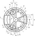
本実施形態の成膜装置100を、図2~図7を参照して説明する。成膜装置100は、個々の電子部品10のパッケージ12の外表面に、スパッタリングにより電磁波シールド膜13を形成する装置である。成膜装置100は、図2に示すように、回転テーブル31が回転すると、保持部33に保持されたトレイ34上の電子部品10が、円周の軌跡で移動して、スパッタ源4に対向する位置を通過するときに、ターゲット41(図3参照)からスパッタされた粒子を付着させて成膜する装置である。
[Film formation device]
The
成膜装置100は、図2及び図3に示すように、チャンバ20、搬送部30、成膜処理部40A、40B、表面処理部50、ロードロック部60、制御装置70を有する。
As shown in FIGS. 2 and 3, the
[チャンバ]
チャンバ20は、反応ガスGが導入される容器である。反応ガスGは、スパッタ用のスパッタガスG1、各種処理用のプロセスガスG2を含む(図4参照)。以下の説明では、スパッタガスG1、プロセスガスG2を区別しない場合には、反応ガスGと呼ぶ場合がある。スパッタガスG1は、電力の印加により生じるプラズマにより、発生するイオン等をターゲット41に衝突させて、電子部品10のパッケージ12にスパッタリングを実施するためのガスである。例えば、アルゴンガス等の不活性ガスを、スパッタガスG1として用いることができる。
[Chamber]
The
プロセスガスG2は、エッチングやアッシングによる表面処理を行うためのガスである。以下、このような表面処理を、逆スパッタと呼ぶ場合がある。プロセスガスG2は、処理の目的によって適宜変更可能である。例えば、エッチングを行う場合は、エッチングガスとしてアルゴンガス等の不活性ガスを用いることができる。本実施形態においては、アルゴンガスによって、電子部品10の表面の洗浄と、粗面化処理を行う。例えば、表面を洗浄およびナノオーダーで粗面化処理を行うことにより、膜の密着力を高めることができる。
The process gas G2 is a gas for performing surface treatment by etching or ashing. Hereinafter, such surface treatment may be referred to as reverse sputtering. The process gas G2 can be appropriately changed depending on the purpose of the treatment. For example, when etching is performed, an inert gas such as argon gas can be used as the etching gas. In the present embodiment, the surface of the
チャンバ20の内部の空間は真空室21を形成している。この真空室21は、気密性があり、減圧により真空とすることができる空間である。例えば、図2及び図4に示すように、真空室21は、チャンバ20の内部の天井20a、内底面20b及び内周面20cによって形成される円柱形状の密閉空間である。
The space inside the
チャンバ20は、図4に示すように、排気口22、導入口24を有する。排気口22は、真空室21と外部との間で気体の流通を確保して、排気Eを行うための開口である。この排気口22は、例えば、チャンバ20の底部に形成されている。排気口22には、排気部23が接続されている。排気部23は、配管及び図示しないポンプ、バルブ等を有する。この排気部23による排気処理により、真空室21内は減圧される。
As shown in FIG. 4, the
導入口24は、真空室21のターゲット41の近傍に、スパッタガスG1を導入するための開口である。この導入口24には、ガス供給部25が接続されている。ガス供給部25は、各ターゲット41に対して1つずつ設けられている。また、ガス供給部25は、配管の他、図示しない反応ガスGのガス供給源、ポンプ、バルブ等を有する。このガス供給部25によって、導入口24から真空室21内にスパッタガスG1が導入される。なお、チャンバ20の上部には、後述するように、表面処理部50が挿入される開口21aが設けられている。
The
[搬送部]
搬送部30は、チャンバ20内に設けられ、電子部品10を円周の軌跡で循環搬送する装置である。循環搬送は、電子部品10を搭載したトレイ34を円周の軌跡で周回移動させることをいう。搬送部30によってトレイ34が移動する軌跡を、搬送経路Lと呼ぶ。搬送部30は、回転テーブル31、モータ32、保持部33を有する。また、保持部33には、載置部35を搭載したトレイ34が保持される。
[Transport section]
The
回転テーブル31は、円形の板である。モータ32は、回転テーブル31に駆動力を与え、円の中心を軸として回転させる駆動源である。保持部33は、搬送部30により搬送される後述するトレイ34を保持する構成部である。回転テーブル31の天面には、複数の保持部33が円周等配位置に配設されている。例えば、各保持部33がトレイ34を保持する領域は、回転テーブル31の周方向の円の接線に平行な向きで形成され、かつ、周方向において等間隔に設けられている。より具体的には、保持部33は、トレイ34を保持する溝、穴、突起、治具、ホルダ等である。メカチャック、粘着チャックによって構成することができる。
The rotary table 31 is a circular plate. The
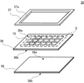
トレイ34は、図5に示すように、平坦な載置面34aを有する部材である。載置面34aは、方形状の平板の一方の平面である。載置面34aの周縁部には、周壁部34bが形成されている。周壁部34bは、載置面34aを囲う方形状に隆起した枠である。トレイ34の材質としては、熱伝導性の高い材質、例えば、金属とすることが好ましい。本実施形態では、トレイ34の材質をSUSとする。なお、トレイ34の材質は、例えば、熱伝導性の良いセラミクスや樹脂、または、それらの複合材としてもよい。
As shown in FIG. 5, the
載置部35は、トレイ34の載置面34aに載置され、電子部品10を搭載するための部材である。載置部35は、保持シート36、フレーム37、密着シート38を有する。保持シート36は、図6に示すように、平坦なシートであり、一方の面に粘着性を有する粘着面36aを有する。粘着面36aは、保持シート36の一方の面の全体に亘る。粘着面36aは、電子部品10を貼り付けるための貼付領域Sを有する。本実施形態では、保持シート36は方形であり、貼付領域Sは保持シート36の外縁よりも小さな方形状の領域である。但し、貼付領域Sを保持シート36の全面とすることもできる。保持シート36の他方の面は、粘着性を有さない非粘着面36bである。非粘着面36bは、例えば、円滑性のある面とすることができる。
The mounting
フレーム37は、保持シート36の粘着面36aが貼り付けられ、貼付領域Sの外縁の一部又は全部を画する部材である。フレーム37の材質としては、熱伝導性の高い材質、例えば、金属とすることが好ましい。本実施形態では、フレーム37の材質をSUSとする。なお、トレイ34と同様に、フレーム37の材質を、例えば、熱伝導性の良いセラミクスや樹脂、または、それらの複合材としてもよい。トレイ34の材質とフレーム37の材質は、一致していても、相違していてもよい。本実施形態のフレーム37は、貼付領域Sを囲み、貼付領域Sの外縁の全部を規定する。フレーム37は、方形状の板状部材であり、中央に方形状の貫通穴37aが形成されている。この貫通穴37aの内縁が、貼付領域Sの外縁に一致する。フレーム37の外形は、保持シート36の外形と一致する。
The
保持シート36の粘着面36aは、フレーム37の底面に、互いの外形が一致して、貫通穴37aの底面側を塞ぐように貼り付けられている。このため、フレーム37の天面側の貫通穴37aからは、粘着面36aの貼付領域Sが露出している。
The
複数の電子部品10は、図5及び図6に示すように、フレーム37内の露出した貼付領域Sの上に粘着保持される。複数の電子部品10は、天面12aのみならず、側面12bにも膜が形成されるように、間隔を空けてマトリクス状に整列配置される。
As shown in FIGS. 5 and 6, the plurality of
密着シート38は、図6に示すように、平坦なシートであり、一方の面に第1の密着面38aを有し、他方の面に第2の密着面38bを有する。第1の密着面38aは、保持シート36の非粘着面36bに密着する粘着性のある面である。第1の密着面38aは、少なくとも貼付領域Sに対応する非粘着面36bの領域の全体に亘って密着している。貼付領域Sに対応する非粘着面36bの領域とは、貼付領域Sの真裏となる非粘着面36bの領域をいう。また、第1の密着面38aは、フレーム37に対応する非粘着面36bの領域にも密着している。つまり、第1の密着面38aは、フレーム37の真裏となる非粘着面36bの領域にも及ぶ範囲に密着している。本実施形態では、フレーム37、保持シート36、密着シート38の外形寸法が一致している。
As shown in FIG. 6, the
第2の密着面38bは、トレイ34の載置面34aに密着する粘着性のある面である。本実施形態は、フレーム37、保持シート36、密着シート38が、全て外形が一致する態様で積層され、第2の密着面38bの全体がトレイ34に密着する。
The
ここで、第1の密着面38aと保持シート36の非粘着面36bとの接着力をFa、第2の密着面38bとトレイ34の載置面34aとの接着力をFbとすると、Fa<Fbである。なお、例えば、2≦(Fb-Fa)とすることが好ましい。また、保持シート36の非粘着面36bの第1の密着面38aに対する剥離抵抗が、トレイ34の載置面34aの第2の密着面38bに対する剥離抵抗よりも小さい材質により形成されている。例えば、Faを0.02~0.03[N/幅25mm]、Fbが4~7[N/幅25mm]とすることが好ましい。但し、本発明は、これらの値には限定されない。また、密着シート38は、熱伝導率を0.1W/(m・K)以上とすることが好ましい。なお、熱伝導率は、高いほど良いが、1W/(m・K)程度あれば良好な冷却効果が得られる。
Here, if the adhesive force between the first
保持シート36、密着シート38の材質としては、耐熱性のある合成樹脂とすることが考えられる。例えば、PET(ポリエチレンテレフタレート)、PEN(ポリエチレンナフタレート)、PI(ポリイミド)などを用いることができるが、これらには限定されない。粘着面36a、第1の密着面38a、第2の密着面38bは、シートの表面に対して接着剤を適用するか、表面に接着性を生じさせた接着面とすることが考えられる。接着剤又は接着面の材質としては、例えば、シリコーン系、アクリル系の樹脂、その他、ウレタン樹脂、エポキシ樹脂など、接着性のある種々の材料を使用できる。
As the material of the holding
図5及び図6に示すように、複数の電子部品10は、載置部35の粘着面36aの貼付領域S内に、マトリクス状に貼り付けられる。このような載置部35を複数用意して、密着シート38を介してトレイ34の載置面34aに載置することにより、密着シート38の第2の密着面38bを載置面34aに密着させる。但し、載置部35は、単一でトレイ34に載置されていてもよい。
As shown in FIGS. 5 and 6, the plurality of
このように、保持部33に保持されるトレイ34、載置部35、密着シート38によって、電子部品10が回転テーブル31上に位置決めされる。なお、本実施形態では、保持部33は6つ設けられているため、回転テーブル31上には60°間隔で6つのトレイ34が保持される。但し、保持部33は、一つであっても、複数であってもよい。
In this way, the
[成膜処理部]
成膜処理部40A、40Bは、搬送部30により搬送される電子部品10に成膜を行う処理部である。以下、複数の成膜処理部40A、40Bを区別しない場合には、成膜処理部40として説明する。成膜処理部40は、図4に示すように、スパッタ源4、区切部44、電源部6を有する。
[Film film processing unit]
The film forming
(スパッタ源)
スパッタ源4は、電子部品10にスパッタリングにより成膜材料を堆積させて成膜する成膜材料の供給源である。スパッタ源4は、ターゲット41、バッキングプレート42、電極43を有する。ターゲット41は、電子部品10に堆積されて膜となる成膜材料によって形成され、搬送経路Lに離隔して対向する位置に設けられている。本実施形態のターゲット41は、図3に示すように、2つのターゲット41A、41Bが搬送方向に直交する方向、つまり回転テーブル31の回転の半径方向に並んでいる。以下、ターゲット41A、41Bを区別しない場合には、ターゲット41とする。ターゲット41の底面側は、搬送部30により移動する電子部品10に、離隔して対向する。なお、回転テーブル31の径方向におけるトレイ34の大きさよりも、2つのターゲット41A、41Bによって、成膜材料を付着させることができる実行領域である処理領域の方が大きい。
(Spatter source)
The
成膜材料は、後述するように、例えば、Cu、Ni、Fe、SUSなどを使用する。但し、スパッタリングにより成膜される材料であれば、種々の材料を適用可能である。また、ターゲット41は、例えば、円柱形状である。但し、長円柱形状、角柱形状等、他の形状であってもよい。
As the film forming material, for example, Cu, Ni, Fe, SUS and the like are used as described later. However, various materials can be applied as long as the material is formed by sputtering. Further, the
バッキングプレート42は、ターゲット41を保持する部材である。電極43は、チャンバ20の外部からターゲット41に電力を印加するための導電性の部材である。なお、スパッタ源4には、必要に応じてマグネット、冷却機構などが適宜具備されている。
The
(区切部)
区切部44は、スパッタ源4により電子部品10が成膜される成膜ポジションM1、M2、表面処理を行う処理ポジションM3を仕切る部材である。以下、成膜ポジションM1、M2を区別しない場合には、成膜ポジションMとして説明する。区切部44は、図3に示すように、搬送経路Lの円周の中心、つまり搬送部30の回転テーブル31の回転中心から、放射状に配設された方形の壁板44a、44bを有する。壁板44a、44bは、例えば、真空室21の天井に、ターゲット41を挟む位置に設けられている。区切部44の下端は、電子部品10が通過する隙間を空けて、回転テーブル31に対向している。この区切部44があることによって、反応ガスG及び成膜材料が真空室21に拡散することを抑制できる。
(Separation section)
The
成膜ポジションMは、スパッタ源4のターゲット41を含み、区切部44で区切られた空間である。より具体的には、図3に示すように、成膜ポジションM1、M2、処理ポジションM3は、平面方向から見て、区切部44の壁板44a、44bと、チャンバ20の内周面20cによって扇形に囲まれた空間である。成膜ポジションM1、M2、処理ポジションM3の水平方向の範囲は、一対の壁板44a、44bによって区切られた領域となる。なお、成膜ポジションMにおけるターゲット41に対向する位置を通過する電子部品10に、成膜材料が膜として堆積する。この成膜ポジションMは、成膜の大半が行われる領域であるが、成膜ポジションMから外れる領域であっても、成膜ポジションMからの成膜材料の漏れはあるため、全く膜の堆積がないわけではない。つまり、成膜が行われる処理領域は、成膜ポジションMよりもやや広い領域となる。
The film formation position M is a space including the
(電源部)
電源部6は、ターゲット41に電力を印加する構成部である。この電源部6によってターゲット41に電力を印加することにより、スパッタガスG1をプラズマ化させ、成膜材料を、電子部品10に堆積させることができる。本実施形態においては、電源部6は、例えば、高電圧を印加するDC電源である。なお、高周波スパッタを行う装置の場合には、RF電源とすることもできる。回転テーブル31は、接地されたチャンバ20と同電位であり、ターゲット41側に高電圧を印加することにより、電位差を発生させている。これにより、可動の回転テーブル31をマイナス電位とするために電源部6と接続する困難さを回避している。
(Power supply part)
The
複数の成膜処理部40は、成膜材料を選択的に堆積させることにより、複数の成膜材料の層から成る膜を形成する。特に、本実施形態では、異なる種類の成膜材料に対応するスパッタ源4を含み、成膜材料を選択的に堆積させることにより、複数種類の成膜材料の層から成る膜を形成する。異なる種類の成膜材料に対応するスパッタ源4を含むとは、全ての成膜処理部40の成膜材料が異なる場合も、複数の成膜処理部40が共通の成膜材料であるが、他がこれと異なる場合も含む。成膜材料を1種ずつ選択的に堆積させるとは、いずれか1種の成膜材料の成膜処理部40が成膜を行う間、他の成膜材料の成膜処理部40は成膜を行わないことをいう。また、成膜中の成膜処理部40または成膜ポジションMとは、成膜処理部40のターゲット41に電力が印加され、電子部品10に成膜が行える状態にある成膜処理部40または成膜ポジションMのことをいう。
The plurality of film forming
本実施形態では、搬送経路Lの搬送方向に、表面処理部50を挟んで、2つの成膜処理部40A、40Bが配設されている。2つの成膜処理部40A、40Bに、成膜ポジションM1、M2が対応している。これらの成膜処理部40A、40Bのうち、成膜処理部40Aは、成膜材料がSUSである。つまり、成膜処理部40Aのスパッタ源4は、SUSから成るターゲット41A、41Bを備えている。他の成膜処理部40Bは、成膜材料がCuである。つまり、成膜処理部40Bのスパッタ源4は、Cuから成るターゲット41A、41Bを備えている。本実施形態では、いずれか一つの成膜処理部40が成膜処理を行っている間は、他の成膜処理部40は、成膜処理を行わない。
In the present embodiment, two film forming
[表面処理部]
表面処理部50は、搬送部30により搬送される電子部品10に表面処理、つまり逆スパッタを行う処理部である。この表面処理部50は、区切部44により仕切られた、処理ポジションM3に設けられている。表面処理部50は、処理ユニット5を有する。この処理ユニット5の構成例を図3及び図4を参照して説明する。
[Surface treatment part]
The
処理ユニット5は、チャンバ20の上部から内部にかけて設けられた筒形電極51を備えている。筒形電極51は、角筒状であり、一端に開口部51aを有し、他端は閉塞されている。筒形電極51は、開口部51aを有する一端が回転テーブル31に向かうように、チャンバ20の天面に設けられた開口21aに絶縁部材52を介して取り付けられている。筒形電極51の側壁はチャンバ20の内部に延在している。
The
筒形電極51の、開口部51aと反対端には、外方へ張り出すフランジ51bが設けられている。絶縁部材52が、フランジ51bとチャンバ20の開口21aの周縁との間に固定されることで、チャンバ20の内部を気密に保っている。絶縁部材52は絶縁性があればよく、特定の材料に限定されないが、例えば、PTFE(ポリテトラフルオロエチレン)等の材料から構成することができる。
A
筒形電極51の開口部51aは、回転テーブル31の搬送経路Lと向かい合う位置に配置される。回転テーブル31は、搬送部30として、電子部品10を搭載したトレイ34を搬送して開口部51aに対向する位置を通過させる。なお、回転テーブル31の径方向におけるトレイ34の大きさよりも、筒形電極51の開口部51aの方が大きい。
The
図3に示すように、筒形電極51は平面方向から見ると回転テーブル31の半径方向における中心側から外側に向けて拡径する扇形になっている。ここでいう扇形とは、扇子の扇面の部分の形を意味する。筒形電極51の開口部51aも、同様に扇形である。回転テーブル31上のトレイ34が開口部51aに対向する位置を通過する速度は、回転テーブル31の半径方向において中心側に向かうほど遅くなり、外側へ向かうほど速くなる。そのため、開口部51aが単なる長方形又は正方形であると、半径方向における中心側と外側とで電子部品10が開口部51aに対向する位置を通過する時間に差が生じる。開口部51aを半径方向における中心側から外側に向けて拡径させることで、開口部51aを通過する時間を一定とすることができ、後述するプラズマ処理を均等にできる。ただし、通過する時間の差が製品上問題にならない程度であれば、長方形又は正方形でもよい。
As shown in FIG. 3, the
上述したように、筒形電極51はチャンバ20の開口21aを貫通し、一部がチャンバ20の外部に露出している。この筒形電極51におけるチャンバ20の外部に露出した部分は、図4に示すように、ハウジング53に覆われている。ハウジング53によってチャンバ20の内部の空間が気密に保たれる。筒形電極51のチャンバ20の内部に位置する部分、すなわち側壁の周囲は、シールド54によって覆われている。
As described above, the
シールド54は、筒形電極51と同軸の扇形の角筒であり、筒形電極51よりも大きい。シールド54はチャンバ20に接続されている。具体的には、シールド54はチャンバ20の開口21aの縁から立設し、チャンバ20の内部に向かって延びた端部は、筒形電極51の開口部51aと同じ高さに位置する。シールド54は、チャンバ20と同様にカソードとして作用するので、電気抵抗の少ない導電性の金属部材で構成すると良い。シールド54はチャンバ20と一体的に成型しても良く、あるいはチャンバ20に固定金具等を用いて取り付けても良い。
The
シールド54は筒形電極51内でプラズマを安定して発生させるために設けられている。シールド54の各側壁は、筒形電極51の各側壁と所定の隙間を介して略平行に延びるように設けられる。隙間が大きくなりすぎると静電容量が小さくなったり、筒形電極51内で発生したプラズマが隙間に入り込んだりしてしまうため、隙間はできるたけ小さいことが望ましい。ただし、隙間が小さくなり過ぎても、筒形電極51とシールド54との間の静電容量が大きくなってしまうため好ましくない。隙間の大きさは、プラズマの発生に必要とされる静電容量に応じて適宜設定すると良い。なお、図4は、シールド54及び筒形電極51の半径方向に延びる2つの側壁面しか図示していないが、シールド54及び筒形電極51の周方向に延びる2つの側壁面の間も、半径方向の側壁面と同じ大きさの隙間が設けられている。
The
また、筒形電極51にはプロセスガス導入部55が接続されている。プロセスガス導入部55は、配管の他、図示しないプロセスガスG2のガス供給源、ポンプ、バルブ等を有する。このプロセスガス導入部55によって、筒形電極51内にプロセスガスG2が導入される。プロセスガスG2は、上記のように、処理の目的によって適宜変更可能である。
Further, a process
筒形電極51には、高周波電圧を印加するためのRF電源56が接続されている。RF電源56の出力側には整合回路であるマッチングボックス57が直列に接続されている。RF電源56はチャンバ20にも接続されている。RF電源56から電圧を印加すると、筒形電極51がアノードとして作用し、チャンバ20、シールド54及び回転テーブル31がカソードとして作用する。マッチングボックス57は、入力側及び出力側のインピーダンスを整合させることで、プラズマの放電を安定化させる。なお、チャンバ20や回転テーブル31は接地されている。チャンバ20に接続されるシールド54も接地される。RF電源56及びプロセスガス導入部55はともに、ハウジング53に設けられた貫通孔を介して筒形電極51に接続する。
An
プロセスガス導入部55から筒形電極51内にプロセスガスG2であるアルゴンガスを導入し、RF電源56から筒形電極51に高周波電圧を印加すると、アルゴンガスがプラズマ化され、電子、イオン及びラジカル等が発生する。
When argon gas, which is a process gas G2, is introduced into the
(ロードロック部)
ロードロック部60は、真空室21の真空を維持した状態で、図示しない搬送手段によって、外部から未処理の電子部品10を載置部35を介して搭載したトレイ34を、真空室21に搬入し、処理済みの電子部品10を載置部35を介して搭載したトレイ34を真空室21の外部へ搬出する装置である。このロードロック部60は、周知の構造のものを適用することができるため、説明を省略する。
(Road lock part)
The
[制御装置]
制御装置70は、成膜装置100の各部を制御する装置である。この制御装置70は、例えば、専用の電子回路若しくは所定のプログラムで動作するコンピュータ等によって構成できる。つまり、真空室21へのスパッタガスG1及びプロセスガスG2の導入および排気に関する制御、電源部6、RF電源56の制御、回転テーブル31の回転の制御などに関しては、その制御内容がプログラムされており、PLCやCPUなどの処理装置により実行されるものであり、多種多様な成膜仕様に対応可能である。
[Control device]
The
具体的に制御される内容としては、成膜装置100の初期排気圧力、スパッタ源4の選択、ターゲット41及び筒形電極51への印加電力、スパッタガスG1及びプロセスガスG2の流量、種類、導入時間及び排気時間、成膜時間、モータ32の回転速度などが挙げられる。
Specifically, the contents to be controlled include the initial exhaust pressure of the
上記のように各部の動作を実行させるための制御装置70の構成を、仮想的な機能ブロック図である図7を参照して説明する。すなわち、制御装置70は、機構制御部71、電源制御部72、記憶部73、設定部74、入出力制御部75を有する。
The configuration of the
機構制御部71は、排気部23、ガス供給部25、プロセスガス導入部55、搬送部30のモータ32、ロードロック部60等の駆動源、バルブ、スイッチ、電源等を制御する処理部である。電源制御部72は、電源部6、RF電源56を制御する処理部である。
The
制御装置70は、いずれか1種の成膜材料の成膜処理部が成膜を行う間、他の成膜材料の成膜処理部は成膜を行わないように成膜処理部40を選択的に制御する。つまり、電源制御部72は、成膜処理部40Aのターゲット41へ電圧を印加して成膜を行う間は、成膜処理部40Bのターゲット41への電圧の印加を行わない。また、成膜処理部40Bのターゲット41へ電圧を印加して成膜を行う間は、成膜処理部40Aのターゲット41への電圧の印加を行わない。
The
記憶部73は、本実施形態の制御に必要な情報を記憶する構成部である。設定部74は、外部から入力された情報を、記憶部73に設定する処理部である。入出力制御部75は、制御対象となる各部との間での信号の変換や入出力を制御するインタフェースである。
The
さらに、制御装置70には、入力装置76、出力装置77が接続されている。入力装置76は、オペレータが、制御装置70を介して成膜装置100を操作するためのスイッチ、タッチパネル、キーボード、マウス等の入力手段である。例えば、成膜を行うスパッタ源4の選択を、入力手段により入力できる。
Further, an
出力装置77は、装置の状態を確認するための情報を、オペレータが視認可能な状態とするディスプレイ、ランプ、メータ等の出力手段である。例えば、成膜を行っているスパッタ源4に対応する成膜ポジションM1、M2、表面処理を行っている処理ポジションM3を、出力装置77に、成膜又は処理を行っていないポジションと区別して表示することができる。
The
[動作]
以上のような本実施形態の動作を、上記の図1~図7に加えて、図8、図9を参照して以下に説明する。なお、図示はしないが、成膜装置100には、コンベア、ロボットアーム等の搬送手段によって、載置部35を介して電子部品10を搭載したトレイ34の搬入、搬送、搬出が行われる。
[motion]
The operation of the present embodiment as described above will be described below with reference to FIGS. 8 and 9 in addition to FIGS. 1 to 7 above. Although not shown, the
電子部品10は、図5、図8(A)に示すように、載置部35におけるフレーム37内の貼付領域S上に、間隔を空けてマトリクス状に並べて貼着される。このような複数の載置部35が、トレイ34の載置面34aに搭載される。これにより、図8(B)に示すように、載置面34aに、密着シート38の第2の密着面38bが密着する。なお、後述するように、載置面34aに貼り付けられた密着シート38、コーティング、塗布又は加工等によって載置面34aに形成された密着シート38のように、載置面34aに設けられた密着シート38に対して、フレーム37に貼り付けられた保持シート36の非粘着面36bを貼り付ける態様であってもよい。つまり、トレイ34に設けられた密着シート38に保持シート36が貼り付けられる等、載置部35がトレイ34に載置される過程で保持シート36と密着シート38とが一体化する構成も、載置部35が保持シート36と密着シート38を有する態様に含まれる。貼り付け、コーティング、塗布又は加工等によって載置面34aに形成された密着シート38の場合は、密着シート38とトレイ34との境界面が第2の密着面38bとなる。
As shown in FIGS. 5 and 8A, the
複数のトレイ34は、ロードロック部60の搬送手段により、チャンバ20内に順次搬入される。回転テーブル31は、空の保持部33を、順次、ロードロック部60からの搬入箇所に移動させる。保持部33は、搬送手段により搬入されたトレイ34を、それぞれ個別に保持する。このようにして、図2及び図3に示すように、成膜対象となる電子部品10を搭載したトレイ34が、回転テーブル31上に全て載置される。
The plurality of
以上のように成膜装置100に導入された電子部品10に対する成膜処理を、図3及び図4を参照して説明する。なお、以下の動作は、表面処理部50によって電子部品10の表面を、洗浄および粗面化した後、成膜処理部40A、40Bによって、電子部品10の表面に、電磁波シールド膜13を形成する例である。電磁波シールド膜13は、SUSの層、Cuの層を、交互に積層することにより形成される。電子部品10に直接形成されるSUSの層は、モールド樹脂、Cuとの密着度を高める下地となる。中間のCuの層は、電磁波を遮蔽する機能を有する層である。最上層のSUSの層は、Cuの錆等を防ぐ保護層である。
The film forming process for the
まず、排気部23は、真空室21を排気して減圧することにより真空にする。回転テーブル31が回転して、所定の回転速度に達する。電子部品10は、処理ユニット5において、筒形電極51の開口部51aに対向する位置を通過する。処理ユニット5では、プロセスガス導入部55から筒形電極51にプロセスガスG2であるアルゴンガスを導入し、RF電源56から筒形電極51に高周波電圧を印加する。高周波電圧の印加によってアルゴンガスがプラズマ化され、電子、イオン及びラジカル等が発生する。プラズマはアノードである筒形電極51の開口部51aから、カソードである回転テーブル31へ流れる。プラズマ中のイオンが開口部51aの下を通過する電子部品10の表面に衝突することで、表面が洗浄および粗面化される。そして、表面処理部50による表面処理時間が経過したら、表面処理部50を停止する。つまり、プロセスガス導入部55からのプロセスガスG2の供給、RF電源56による電圧の印加を停止する。
First, the
次に、成膜処理部40Aのガス供給部25は、スパッタガスG1を、ターゲット41の周囲に供給する。この状態下で、保持部33に保持された電子部品10は、搬送経路L上を円を描く軌跡で移動して、スパッタ源4に対向する位置を通過する。
Next, the
次に、成膜処理部40Aのみ、電源部6がターゲット41に電力を印加する。これにより、スパッタガスG1がプラズマ化する。スパッタ源4において、プラズマにより発生したイオンは、ターゲット41に衝突して成膜材料の粒子を飛ばす。このため、成膜処理部40Aの成膜ポジションM1を通過する電子部品10の表面には、その通過毎に成膜材料の粒子が堆積されて、膜が生成される。ここでは、SUSの層が形成される。このとき、電子部品10は成膜処理部40Bの成膜ポジションM2を通過するが、成膜処理部40Bはターゲット41に電力が印加されていないので、成膜処理は行われず、電子部品10は加熱されない。また、成膜ポジションM1、M2以外の領域においても、電子部品10は加熱されない。このように、加熱されない領域において、電子部品10は熱を放出する。
Next, only in the film forming
成膜処理部40Aによる成膜時間が経過したら、成膜処理部40Aを停止する。つまり、電源部6によるターゲット41への電力の印加を停止する。そして、成膜処理部40Bの電源部6が、ターゲット41に電力を印加する。これにより、スパッタガスG1がプラズマ化する。スパッタ源4において、プラズマにより発生したイオンは、ターゲット41に衝突して成膜材料の粒子を飛ばす。このため、成膜処理部40Bの成膜ポジションM2を通過する電子部品10の表面には、その通過毎に成膜材料の粒子が堆積されて、膜が生成される。ここでは、Cuの層が形成される。この層は、電磁波シールド膜13の層の一部となる。このとき、電子部品10は成膜処理部40Aの成膜ポジションM1を通過するが、成膜処理部40Aはターゲット41に電力が印加されていないので、成膜処理を行われず、電子部品10は加熱されない。また、成膜ポジションM1、M2以外の領域においても、電子部品10は加熱されない。このように、加熱されない領域において、電子部品10は熱を放出する。
After the film forming time by the film forming
成膜処理部40Bによる成膜時間が経過したら、成膜処理部40Bを停止する。つまり、電源部6によるターゲット41への電力の印加を停止する。そして、成膜処理部40Aの電源部6が、ターゲット41に電力を印加する。これにより、スパッタガスG1がプラズマ化する。スパッタ源4において、プラズマにより発生したイオンは、ターゲット41に衝突して成膜材料の粒子を飛ばす。このため、成膜処理部40Aの成膜ポジションM1を通過する電子部品10の表面には、その通過毎に成膜材料の粒子が堆積されて、膜が生成される。ここでは、SUSの層が形成される。このとき、電子部品10は成膜処理部40Bの成膜ポジションM2を通過するが、成膜処理部40Bはターゲット41に電力が印加されていないので、成膜処理を行われず、電子部品10は加熱されない。また、成膜ポジションM1、M2以外の領域においても、電子部品10は加熱されない。このように、加熱されない領域において、電子部品10は熱を放出する。
After the film forming time by the film forming
成膜処理部40Aによる成膜時間が経過したら、成膜処理部40Aを停止する。つまり、電源部6によるターゲット41への電力の印加を停止する。このように、成膜処理部40A、40Bによる成膜を繰り返すことにより、SUSの膜、Cuの膜、SUSの膜が積層された膜を形成する。なお、さらに、同様の成膜を繰り返すことにより、3層より多い膜を形成することもできる。これにより、図9(A)に示す状態から、図9(B)に示すように、電子部品10のパッケージ12の天面及び側面に、電磁波シールド膜13が形成される。
After the film forming time by the film forming
以上のような成膜処理の間、回転テーブル31は回転を継続し電子部品10を搭載したトレイ34を循環搬送し続ける。そして、成膜処理が完了した後、電子部品10を搭載したトレイ34は、回転テーブル31の回転により、順次、ロードロック部60に位置決めされ、搬送手段により、外部へ搬出される。図8(C)に示すように、搬出されたトレイ34から載置部35が、保持シート36が密着シート38から剥がされることによって剥がされる。つまり、載置部35から密着シート38が分離される。このように、トレイ34に残留した密着シート38は、そのまま再利用することができる。つまり、次に処理する電子部品10を搭載した保持シート36の非粘着面36bを、トレイ34上の密着シート38の第1の密着面38aに密着させて、トレイ34を真空室21内に搬入することにより、上記と同様に成膜処理を行うことができる。このような態様であっても、保持シート36が密着シート38に貼り付けられることにより、密着シート38を含む載置部35が構成され、載置部35を有する成膜装置100が構成されることになる。複数回の使用で、密着シート38の粘着力が低下してきたら、トレイ34から密着シート38を剥がし、新たな密着シート38を含む載置部35をトレイ34に載置してもよい。密着シート38の使用可能な回数は実験などにより設定しておくことができる。密着シート38を替える場合、密着シート38のみ新しいものにして、保持シート36及びフレーム37については、双方を再利用しても、いずれか一方のみ再利用して他方を新しくしても、双方とも新しいものを使用してもよい。なお、保持シート36を剥がした後に、密着シート38を再利用せずに、トレイ34から密着シート38を剥がして、使い捨てにしても良い。つまり、毎回、トレイ34に残った密着シート38を剥がして廃棄し、密着シート38を含む載置部35を、トレイ34に載置するようにしても良い。
During the film forming process as described above, the rotary table 31 continues to rotate and continues to circulate and convey the
[電子部品の加熱が進行する原因]
上記のように、電子部品10は、加熱されない領域において熱を放出することができる。この熱の放出は、主として、載置部35を介してトレイ34に熱が伝導することにより行われる。但し、本実施形態のように、密着シート38を有さない場合、以下のような問題が生じる。
[Causes of heating of electronic components]
As described above, the
(1)載置部35の保持シート36の底面に粘着性がない場合
載置部35の保持シート36の上面には、電子部品10が貼り付けられる粘着面36aが設けられているが、保持シート36の底面は、粘着性を有していない。このため、単に、載置部35をトレイ34の載置面34aに載置しただけでは、保持シート36の底面と載置面34aとの間に隙間が生じる。つまり、保持シート36の表面と載置面34aの表面には、微細な凹凸があるので、接触している面積は全体の10%程度となってしまう。接触していない空間は、真空であるため熱伝導がない。このため、電子部品10の熱がトレイ34に伝達し難くなる。
(1) When the bottom surface of the holding
(2)載置部35の保持シート36の底面に粘着性がある場合
上記の(1)の問題に対処するため、保持シート36の底面に粘着性を持たせることが考えられる。すると、載置部35をトレイ34の載置面34aに密着させることができ、保持シート36の底面と載置面34aとの間の隙間が大幅に減少するため、熱伝導性が向上する。しかし、この場合、成膜処理後、トレイ34の載置面34aから載置部35の保持シート36の底面を引き剥がす工程が必要となる。載置面34aから載置部35を引き剥がす際に、粘着した面に均一に力を伝達することは困難なため、引き剥がす力が一部に加わって、フレーム37、保持シート36が歪む可能性がある。このようにフレーム37や保持シート36が歪むと、電子部品10の配置面の平坦度が失われたり、電子部品10の配置間隔にばらつきが生じたりするため、後のピックアップ等の工程に支障を来す。
(2) When the bottom surface of the holding
また、電子部品10を保持シート36からピックアップする際には、保持シート36の底面から一個ずつピンで突き上げて剥がすため、底面に粘着性があると、ピンに粘着剤が付着して、ピンの接触位置、接触面積が変化することにより、正確なピックアップができない。さらに、接触させたピンを保持シート36から引き離す際に、保持シート36がピンに付着したまま引っ張られ、その後、保持シート36の張力に粘着剤の粘着力が負けて剥がれ、これによって弾かれてしまうと、電子部品10に位置ずれや剥離などの影響を与える可能性がある。
Further, when the
[電子部品の放熱が向上する理由]
本実施形態では、載置部35の保持シート36の粘着面36aの反対側の面は粘着性を有さない非粘着面36bである。しかしながら、この保持シート36を、密着シート38を介して、トレイ34の載置面34aに密着させている。このため、電子部品10の熱が、保持シート36、密着シート38を介して、トレイ34に伝達される。従って、電子部品10の加熱が抑制される。
[Reason for improving heat dissipation of electronic components]
In the present embodiment, the surface opposite to the
また、第1の密着面38aと非粘着面36bとの接着力が、第2の密着面38bと載置面34aとの接着力より小さい。このため、トレイ34から保持シート36を離脱させる際に、第2の密着面38bが載置面34aに密着した状態で、第1の密着面38aから保持シート36が容易に剥がれる。したがって、フレーム37、保持シート36が歪み難い。保持シート36の粘着面36aと反対側が非粘着面36bであるため、電子部品10をピックアップする際に、保持シート36がピンに付着する問題も生じない。
Further, the adhesive force between the first
[作用効果]
本実施形態は、スパッタガスG1が導入される容器であるチャンバ20と、チャンバ20内に設けられ、電子部品10を循環搬送する搬送部30と、搬送部30により循環搬送される電子部品10に、スパッタリングにより成膜材料を堆積させて成膜するスパッタ源4を有するとともに、スパッタ源4により電子部品10に成膜する成膜処理部40と、搬送部30により搬送され、載置面34aを有するトレイ34と、載置面34aに載置され、電子部品10を搭載するための載置部35と、を有する。
[Action effect]
In this embodiment, the
載置部35は、一方の面に粘着性を有する粘着面36aを有し、他方の面に粘着性を有さない非粘着面36bを有する保持シート36と、一方の面に、非粘着面36bに密着する粘着性のある第1の密着面38aを有し、他方の面に、トレイ34の載置面34aに密着する粘着性のある第2の密着面38bを有する密着シート38と、を有し、粘着面36aは、電子部品10を貼り付けるための貼付領域Sを有し、少なくとも貼付領域Sに対応する非粘着面36bの領域の全体に亘って、第1の密着面38aが密着している。
The mounting
このため、電子部品10からの熱が、保持シート36及び密着シート38を介して、トレイ34に伝達されて効率良く放熱されるので、装置構成を複雑化、大型化することなく、電子部品10の加熱を抑制できる。また、冷却のために電力を使用する必要がなく、メンテナンスも容易となる。
Therefore, the heat from the
保持シート36の粘着面36aには、貼付領域Sの外縁の一部又は全部を規定するフレーム37が貼り付けられ、第1の密着面38aは、貼付領域Sに対応する非粘着面36bの領域の全体に加えて、さらにフレーム37に対応する非粘着面36bの領域にも密着している。
A
このため、フレーム37からの熱も、保持シート36及び密着シート38を介して、トレイ34に伝達されて効率良く放熱される。フレーム37は、保持シート36に比べて硬質であるため、密着シート38から保持シート36を剥離する際に、フレーム37に囲まれた貼付領域Sが安定し、電子部品10への影響を抑えることができる。但し、成膜処理等において、フレーム37も電子部品10と同様に加熱される。本実施形態では、密着シート38による冷却効果を、フレーム37についても得ることができる。
Therefore, the heat from the
また、第1の密着面38aと非粘着面36bとの接着力をFa、第2の密着面38bと載置面34aとの接着力をFbとすると、Fa<Fbである。より好ましくは、第1の密着面38aの非粘着面36bに対する剥離抵抗が、第2の密着面38bの載置面34aに対する剥離抵抗よりも、小さい材質により形成されている。
Further, when the adhesive force between the
このため、載置部35から密着シート38を分離する際に、密着シート38がトレイ34側に残り、保持シート36を剥離し易くなる。保持シート36を密着シート38から軽い力で剥離することができるので、保持シート36の変形を抑制することができる。
Therefore, when the
また、密着シート38は、熱伝導率が0.1W/(m・K)以上である。これにより、電子部品10の放熱が促進され、加熱が防止される。
Further, the
[試験結果]
本実施形態の成膜装置と比較例の成膜装置を用いて、上記のような手順で実際に成膜処理の動作を実施して、温度を測定した試験結果を以下に説明する。但し、載置部には電子部品を載置していない。温度は、フィルムの温度≒電子部品の温度と見立てて、保持シートの温度を熱電対で測定した。電磁波シールド膜の各層の成膜条件は、図10に示す通りである。なお、Arボンバードとは、イオンボンバードメントとも言い、Arによる洗浄、粗面化処理であり、上記の表面処理に相当する。
[Test results]
The test results of actually performing the film forming process operation by the above procedure using the film forming apparatus of the present embodiment and the film forming apparatus of the comparative example and measuring the temperature will be described below. However, no electronic components are mounted on the mounting section. The temperature was assumed to be the temperature of the film ≈ the temperature of the electronic component, and the temperature of the holding sheet was measured with a thermocouple. The film forming conditions for each layer of the electromagnetic wave shielding film are as shown in FIG. The Ar bombard is also referred to as an ion bombardment, which is a cleaning and roughening treatment with Ar, and corresponds to the above-mentioned surface treatment.
(比較例)
比較例では、保持シートとして、PETフィルムを用い、密着シートを用いずに成膜を行った。この結果を、図11に示す。この試験では、表面処理により50℃程度まで上昇し、下地層のSUSの成膜で80℃程度、さらに、Cuの成膜で145℃程度まで上昇した。その後の保護層のSUSの成膜では、110℃程度まで下降した。
(Comparative example)
In the comparative example, a PET film was used as the holding sheet, and the film was formed without using the adhesion sheet. The result is shown in FIG. In this test, the temperature rose to about 50 ° C. due to the surface treatment, to about 80 ° C. for the SUS film formation of the base layer, and further to about 145 ° C. for the Cu film formation. Subsequent film formation of SUS in the protective layer lowered the temperature to about 110 ° C.
一般的な半導体パッケージは、150℃を超えると、パッケージを構成する樹脂が破壊されやすくなる。このため、150℃に近い145℃程度まで加熱されてしまうことは好ましくない。特に、100℃を超えると、保持シートと密着シートから、水分や接着剤のガス放出が発生し、抵抗値が上がる等、膜質を劣化させる可能性がある。このため、このような成膜装置の場合、冷却機構があることが好ましい。 In a general semiconductor package, when the temperature exceeds 150 ° C., the resin constituting the package is easily destroyed. Therefore, it is not preferable to heat up to about 145 ° C, which is close to 150 ° C. In particular, if the temperature exceeds 100 ° C., moisture and adhesive gas are released from the holding sheet and the adhesive sheet, which may increase the resistance value and deteriorate the film quality. Therefore, in the case of such a film forming apparatus, it is preferable to have a cooling mechanism.
(実施例)
実施例では、保持シートとしてPETフィルムを用い、密着シートとしてPETフィルムを用いて成膜を行った。この結果を図12に示す。この試験では、表面処理においては、35℃程度の上昇にとどまり、下地層のSUSの成膜で40℃程度、さらに、Cuの成膜で60℃程度までしか上昇しなかった。その後の保護層のSUSの成膜では、50℃程度まで下降した。このように、本発明では、温度上昇が大幅に抑えられることが分かる。なお、図11、図12では、ノイズが入った関係で、微細な時間間隔で測定値が上下に変動している箇所があるが、全体の傾向としては変わらない。
(Example)
In the examples, a PET film was used as the holding sheet, and a PET film was used as the adhesion sheet to form a film. The result is shown in FIG. In this test, in the surface treatment, the temperature rose only to about 35 ° C., to about 40 ° C. for the SUS film formation of the underlayer, and to about 60 ° C. for the Cu film formation. Subsequent film formation of SUS in the protective layer lowered the temperature to about 50 ° C. As described above, it can be seen that the temperature rise is significantly suppressed in the present invention. In addition, in FIGS. 11 and 12, there are places where the measured value fluctuates up and down at minute time intervals due to noise, but the overall tendency does not change.
[他の実施形態]
本発明は、上記の実施形態に限定されるものではなく、以下のような態様も含む。
(1)上記の実施形態では、保持シート36、密着シート38を平坦としているが、これは平板状であることを意味し、その表面が平らであることには限定されない。保持シート36の粘着面36a、密着シート38の第1の密着面38a、第2の密着面38bは、粘着性のある面であるため、微細な凹凸が存在する。さらに、密着シート38の第1の密着面38a、第2の密着面38bを、溝を持つ形状としても良い。例えば、第1の密着面38a及び第2の密着面38bの一方又は双方に、外部と連通した溝を形成する。溝は、冷却効果を阻害しない程度に小さいことが好ましい。このような溝を設けることで、保持シート36と密着シート38とを貼り合せた際に、密着面に気泡が形成されたとしても、溝から気泡が抜けやすくなる効果がある。また、この場合、密着シート38における溝で区切られた形状は、四角形等の多角形状としても、円形、楕円形等の閉曲線形状としてもよい。さらに、トレイ34の載置面34aも、平坦面には限定されない。載置面34aと密着シート38の第2の密着面38bのそれぞれに互いに合致する凹凸を形成しておき、表面積の拡大による熱伝導性の向上を図ってもよい。
[Other embodiments]
The present invention is not limited to the above embodiment, but also includes the following aspects.
(1) In the above embodiment, the holding
(2)成膜材料については、スパッタリングにより成膜可能な種々の材料を適用可能である。例えば、電磁波シールド膜としては、Al、Ag、Ti、Nb、Pd、Pt、Zr等を用いることもできる。さらに、磁性体として、Ni、Fe、Cr、Co等を使用することができる。さらに、また、下地の密着層として、SUS、Ni、Ti、V、Ta等を用いたり、最表面の保護層として、SUS、Au等を用いることができる。 (2) As the film forming material, various materials that can be formed by sputtering can be applied. For example, as the electromagnetic wave shielding film, Al, Ag, Ti, Nb, Pd, Pt, Zr and the like can also be used. Further, Ni, Fe, Cr, Co and the like can be used as the magnetic material. Furthermore, SUS, Ni, Ti, V, Ta and the like can be used as the underlying adhesion layer, and SUS, Au and the like can be used as the outermost protective layer.
(3)パッケージ12の形態は、例えば、BGA、LGA、SОP、QFP、WLPなど、現在又は将来において利用可能なあらゆる形態が適用可能である。電子部品10が外部との電気的な接続を行う端子としても、例えば、底面に設けるBGA等の半球状のものやLGA等の平面状のもの、側面に設けるSОP、QFPの細板状のもの等が考えられるが、現在又は将来において利用可能なあらゆる端子が適用可能であり、その形成位置も問わない。また、電子部品10の内部に封止される素子11は、単数であっても複数であってもよい。
(3) As the form of the
(4)成膜ポジションにおけるターゲットの数は、2つには限定されない。ターゲットを1つとしても、3つ以上としてもよい。また、成膜ポジションも2つ以下としても、4つ以上としてもよい。 (4) The number of targets in the film formation position is not limited to two. The number of targets may be one or three or more. Further, the film formation position may be two or less, or four or more.
(5)搬送部により同時搬送されるトレイ、電子部品の数、これを保持する保持部の数は、少なくとも1つであればよく、上記の実施形態で例示した数には限定されない。つまり、1つの電子部品が循環して成膜を繰り返す態様でもよく、2つ以上の電子部品が循環して成膜を繰り返す態様でもよい。 (5) The number of trays and electronic components simultaneously conveyed by the conveying unit and the number of holding units for holding the trays may be at least one, and the number is not limited to the number exemplified in the above embodiment. That is, one electronic component may circulate and repeat the film formation, or two or more electronic components may circulate and repeat the film formation.
(6)エッチングやアッシングによる洗浄や表面処理は、成膜ポジションを有するチャンバとは別のチャンバで行ってもよい。なお、酸化処理又は後酸化処理を行う場合は、プロセスガスG2として酸素を用いることができる。窒化処理を行う場合は、プロセスガスG2として窒素を用いることができる。 (6) Cleaning and surface treatment by etching or ashing may be performed in a chamber different from the chamber having the film forming position. When the oxidation treatment or the post-oxidation treatment is performed, oxygen can be used as the process gas G2. When nitriding is performed, nitrogen can be used as the process gas G2.
(7)上記の実施形態では、回転テーブル31が水平面内で回転する例としている。但し、搬送部の回転面の向きは、特定の方向には限定されない。例えば、垂直面内で回転する回転面とすることもできる。さらに、搬送部が有する搬送手段は、回転テーブルには限定されない。例えば、ワークを保持する保持部を有する円筒形状の部材が、軸を中心に回転する回転体としてもよい。また、循環搬送の軌跡は、円周には限定されない。無端状の搬送経路により、循環搬送される態様を広く含む。例えば、矩形や楕円であってもよいし、クランクや蛇行する経路を含んでいてもよい。搬送経路は、例えば、コンベア等により構成してもよい。 (7) In the above embodiment, the rotary table 31 rotates in a horizontal plane. However, the direction of the rotating surface of the transport unit is not limited to a specific direction. For example, it may be a rotating surface that rotates in a vertical surface. Further, the transport means included in the transport unit is not limited to the rotary table. For example, a cylindrical member having a holding portion for holding a work may be a rotating body that rotates about an axis. Further, the locus of circulation transportation is not limited to the circumference. It includes a wide range of modes in which circulation is carried out by an endless transport path. For example, it may be rectangular or elliptical, and may include a crank or a meandering path. The transport path may be configured by, for example, a conveyor or the like.
さらに、本発明は、スパッタガスG1が導入される容器であるチャンバ20と、チャンバ20内に設けられ、スパッタリングにより成膜材料を堆積させて成膜するスパッタ源4を有するとともに、スパッタ源4により電子部品10に成膜する成膜処理部40と、成膜処理部40による処理領域に設置され、載置面34aを有するトレイ34と、載置面34aに載置され、電子部品10を搭載するための載置部35とを有する成膜装置100であて、上記のような載置部35を有していればよい。このため、電子部品10を循環搬送せずに、静止した状態で成膜する成膜装置であってもよい。載置部35を介して電子部品10を搭載したトレイ34を搬入して、処理領域に設置し、ターゲット41に対する相対位置を変化させずにスパッタリングを行ってもよい。
Further, the present invention has a
(8)上記の実施形態では、成膜材料を1種ずつ選択的に堆積させて成膜するようにしている。しかし、本発明はこれに限るものではなく、成膜材料を選択的に堆積させることにより、複数の成膜材料の層から成る膜を形成できればよい。このため、2種以上の成膜材料を同時に堆積させるようにしても良い。例えば、電磁波シールド膜を、Co、Zr、Nbの合金で形成することがある。このような場合に、複数の成膜処理部のうち、Coを成膜材料とする成膜処理部と、Zrを成膜材料とする成膜処理部とNbを成膜材料とする成膜処理部を同時に選択して成膜を行なうようにしても良い。 (8) In the above embodiment, the film-forming materials are selectively deposited one by one to form a film. However, the present invention is not limited to this, and it is sufficient that a film composed of a plurality of layers of the film-forming material can be formed by selectively depositing the film-forming material. Therefore, two or more kinds of film forming materials may be deposited at the same time. For example, the electromagnetic wave shielding film may be formed of an alloy of Co, Zr, and Nb. In such a case, among a plurality of film forming processing sections, a film forming processing section using Co as a film forming material, a film forming processing section using Zr as a film forming material, and a film forming process using Nb as a film forming material. The portions may be selected at the same time to form a film.
そしてこの場合、円周の軌跡のうち、これらの成膜中に成膜ポジションを通過する軌跡よりも、成膜中の成膜ポジション以外の部分を通過する軌跡の方が長くなるように、成膜に用いる成膜処理部を選択する、あるいは、成膜処理部を区切る区切部の配置を設定すると良い。 In this case, the circumferential locus is formed so that the locus passing through a portion other than the film forming position during film formation is longer than the locus passing through the film forming position during film formation. It is preferable to select the film forming processing section to be used for the film, or to set the arrangement of the dividing section that separates the film forming processing section.
つまり、1種、または、複数種の成膜処理部を複数個選択して成膜を行なう場合、或いは単一の成膜処理部を選択して成膜を行なう場合のいずれにおいても、円周の軌跡のうち、成膜中に成膜ポジションを通過する軌跡よりも、成膜中の成膜ポジション以外の部分を通過する軌跡の方が長くなるように、成膜に用いる成膜処理部を選択する、あるいは、成膜処理部を区切る区切部の配置を設定すると良い。 That is, in either case of selecting a plurality of one-type or a plurality of types of film-forming processing sections to form a film, or selecting a single film-forming processing section to form a film, the circumference Of the trajectories, the film formation processing unit used for film formation is provided so that the trajectory that passes through the portion other than the film formation position during film formation is longer than the trajectory that passes through the film formation position during film formation. It is preferable to select or set the arrangement of the dividing portion that separates the film forming processing portion.
(9)以上、本発明の実施形態及び各部の変形例を説明したが、この実施形態や各部の変形例は、一例として提示したものであり、発明の範囲を限定することは意図していない。上述したこれら新規な実施形態は、その他の様々な形態で実施されることが可能であり、発明の要旨を逸脱しない範囲で、種々の省略、置き換え、変更を行うことができる。これら実施形態やその変形は、発明の範囲や要旨に含まれるとともに、特許請求の範囲に記載された発明に含まれる。 (9) Although the embodiments of the present invention and modified examples of each part have been described above, the embodiments and modified examples of each part are presented as examples, and the scope of the invention is not intended to be limited. .. These novel embodiments described above can be implemented in various other embodiments, and various omissions, replacements, and changes can be made without departing from the gist of the invention. These embodiments and variations thereof are included in the scope and gist of the invention, and are also included in the invention described in the claims.
10 電子部品
11 素子
12 パッケージ
13 電磁波シールド膜
14 基板
100 成膜装置
20 チャンバ
20a 天井
20b 内底面
20c 内周面
21 真空室
22 排気口
23 排気部
24 導入口
25 ガス供給部
30 搬送部
31 回転テーブル
32 モータ
33 保持部
34 トレイ
34a 載置面
34b 周壁部
35 載置部
36 保持シート
36a 粘着面
36b 非粘着面
37 フレーム
37a 貫通穴
38 密着シート
38a 第1の密着面
38b 第2の密着面
40、40A、40B 成膜処理部
4 スパッタ源
41、41A、41B ターゲット
42 バッキングプレート
43 電極
44 区切部
44a、44b 壁板
5 処理ユニット
51 筒形電極
51a 開口部
51b フランジ
52 絶縁部材
53 ハウジング
54 シールド
55 プロセスガス導入部
56 RF電源
57 マッチングボックス
6 電源部
60 ロードロック部
70 制御装置
71 機構制御部
72 電源制御部
73 記憶部
74 設定部
75 入出力制御部
76 入力装置
77 出力装置
E 排気
L 搬送経路
M、M1、M2 成膜ポジション
M3 処理ポジション
G 反応ガス
G1 スパッタガス
G2 プロセスガス
S 貼付領域
10
Claims (6)
前記チャンバ内に設けられ、スパッタリングにより成膜材料を堆積させて成膜するスパッタ源を有するとともに、前記スパッタ源により電子部品に成膜する成膜処理部と、
前記成膜処理部による処理領域に設置され、載置面を有するトレイと、
前記載置面に載置され、前記電子部品を搭載するための載置部と、
を有し、
前記載置部は、
一方の面に粘着性を有する粘着面を有し、他方の面に粘着性を有さない非粘着面を有する保持シートと、
一方の面に、前記非粘着面に密着する粘着性のある第1の密着面を有し、他方の面に、前記トレイの載置面に密着する粘着性のある第2の密着面を有する密着シートと、
を有し、
前記粘着面は、前記電子部品を貼り付けるための貼付領域を有し、
少なくとも前記貼付領域に対応する非粘着面の領域の全体に亘って、前記第1の密着面が密着しており、
前記第1の密着面と前記非粘着面との間の接着力をFa、前記第2の密着面と前記載置面との間の接着力をFbとしたとき、Fa<Fbであることを特徴とする成膜装置。 The chamber, which is the container into which the sputter gas is introduced, and
A film forming processing unit provided in the chamber, which has a sputtering source for depositing a film forming material by sputtering to form a film, and a film forming processing unit for forming a film on an electronic component by the sputtering source.
A tray installed in the processing area of the film forming processing unit and having a mounting surface,
A mounting portion mounted on the mounting surface described above for mounting the electronic component, and a mounting portion.
Have,
The above-mentioned place is
A holding sheet having an adhesive surface on one surface and a non-adhesive surface on the other surface,
One surface has a first adhesive surface that adheres to the non-adhesive surface, and the other surface has a second adhesive surface that adheres to the mounting surface of the tray. Adhesive sheet and
Have,
The adhesive surface has a sticking area for sticking the electronic component.
The first contact surface is in close contact with at least the entire non-adhesive surface area corresponding to the sticking area .
When the adhesive force between the first adhesive surface and the non-adhesive surface is Fa, and the adhesive force between the second adhesive surface and the above-mentioned mounting surface is Fb, Fa <Fb. A featured film forming device.
前記チャンバ内に設けられ、電子部品を循環搬送する搬送部と、
前記搬送部により循環搬送される前記電子部品に、スパッタリングにより成膜材料を堆積させて成膜するスパッタ源を有するとともに、前記スパッタ源により電子部品に成膜する成膜処理部と、
前記搬送部により搬送され、載置面を有するトレイと、
前記載置面に載置され、前記電子部品を搭載するための載置部と、
を有し、
前記載置部は、
一方の面に粘着性を有する粘着面を有し、他方の面に粘着性を有さない非粘着面を有する保持シートと、
一方の面に、前記非粘着面に密着する粘着性のある第1の密着面を有し、他方の面に、前記トレイの載置面に密着する粘着性のある第2の密着面を有する密着シートと、
を有し、
前記粘着面は、前記電子部品を貼り付けるための貼付領域を有し、
少なくとも前記貼付領域に対応する非粘着面の領域の全体に亘って、前記第1の密着面が密着しており、
前記第1の密着面と前記非粘着面との間の接着力をFa、前記第2の密着面と前記載置面との間の接着力をFbとしたとき、Fa<Fbであることを特徴とする成膜装置。 The chamber, which is the container into which the sputter gas is introduced, and
A transport unit provided in the chamber for circulating and transporting electronic components,
The electronic component that is circulated and transported by the transport unit has a sputter source for depositing a film forming material by sputtering to form a film, and a film forming processing unit for forming a film on the electronic component by the sputtering source.
A tray that is transported by the transport unit and has a mounting surface,
A mounting portion mounted on the mounting surface described above for mounting the electronic component, and a mounting portion.
Have,
The above-mentioned place is
A holding sheet having an adhesive surface on one surface and a non-adhesive surface on the other surface,
One surface has a first adhesive surface that adheres to the non-adhesive surface, and the other surface has a second adhesive surface that adheres to the mounting surface of the tray. Adhesive sheet and
Have,
The adhesive surface has a sticking area for sticking the electronic component.
The first contact surface is in close contact with at least the entire non-adhesive surface area corresponding to the sticking area .
When the adhesive force between the first adhesive surface and the non-adhesive surface is Fa, and the adhesive force between the second adhesive surface and the above-mentioned mounting surface is Fb, Fa <Fb. A featured film forming device.
前記チャンバ内に設けられ、スパッタリングにより成膜材料を堆積させて成膜するスパッタ源を有するとともに、前記スパッタ源により電子部品に成膜する成膜処理部と、A film forming processing unit provided in the chamber, which has a sputtering source for depositing a film forming material by sputtering to form a film, and a film forming processing unit for forming a film on an electronic component by the sputtering source.
前記成膜処理部による処理領域に設置され、載置面を有するトレイと、A tray installed in the processing area of the film forming processing unit and having a mounting surface,
前記載置面に載置され、前記電子部品を搭載するための載置部と、A mounting portion mounted on the mounting surface described above for mounting the electronic component, and a mounting portion.
を有し、Have,
前記載置部は、The above-mentioned place is
一方の面に粘着性を有する粘着面を有し、他方の面に粘着性を有さない非粘着面を有する保持シートと、A holding sheet having an adhesive surface on one surface and a non-adhesive surface on the other surface,
一方の面に、前記非粘着面に密着する粘着性のある第1の密着面を有し、他方の面に、前記トレイの載置面に密着する粘着性のある第2の密着面を有する密着シートと、One surface has a first adhesive surface that adheres to the non-adhesive surface, and the other surface has a second adhesive surface that adheres to the mounting surface of the tray. Adhesive sheet and
を有し、Have,
前記粘着面は、前記電子部品を貼り付けるための貼付領域を有し、The adhesive surface has a sticking area for sticking the electronic component.
少なくとも前記貼付領域に対応する非粘着面の領域の全体に亘って、前記第1の密着面が密着しており、The first contact surface is in close contact with at least the entire non-adhesive surface area corresponding to the sticking area.
前記密着シートは、前記第1の密着面の前記非粘着面に対する剥離抵抗が、前記第2の密着面の前記載置面に対する剥離抵抗よりも小さい材質により形成されていることを特徴とする成膜装置。The adhesive sheet is characterized in that the peeling resistance of the first adhesive surface to the non-adhesive surface is smaller than the peeling resistance of the second adhesive surface to the previously described mounting surface. Membrane device.
前記チャンバ内に設けられ、電子部品を循環搬送する搬送部と、A transport unit provided in the chamber for circulating and transporting electronic components,
前記搬送部により循環搬送される前記電子部品に、スパッタリングにより成膜材料を堆積させて成膜するスパッタ源を有するとともに、前記スパッタ源により電子部品に成膜する成膜処理部と、The electronic component that is circulated and transported by the transport unit has a sputter source for depositing a film forming material by sputtering to form a film, and a film forming processing unit for forming a film on the electronic component by the sputtering source.
前記搬送部により搬送され、載置面を有するトレイと、A tray that is transported by the transport unit and has a mounting surface,
前記載置面に載置され、前記電子部品を搭載するための載置部と、A mounting portion mounted on the mounting surface described above for mounting the electronic component, and a mounting portion.
を有し、Have,
前記載置部は、The above-mentioned place is
一方の面に粘着性を有する粘着面を有し、他方の面に粘着性を有さない非粘着面を有する保持シートと、A holding sheet having an adhesive surface on one surface and a non-adhesive surface on the other surface,
一方の面に、前記非粘着面に密着する粘着性のある第1の密着面を有し、他方の面に、前記トレイの載置面に密着する粘着性のある第2の密着面を有する密着シートと、One surface has a first adhesive surface that adheres to the non-adhesive surface, and the other surface has a second adhesive surface that adheres to the mounting surface of the tray. Adhesive sheet and
を有し、Have,
前記粘着面は、前記電子部品を貼り付けるための貼付領域を有し、The adhesive surface has a sticking area for sticking the electronic component.
少なくとも前記貼付領域に対応する非粘着面の領域の全体に亘って、前記第1の密着面が密着しており、The first contact surface is in close contact with at least the entire non-adhesive surface area corresponding to the sticking area.
前記密着シートは、前記第1の密着面の前記非粘着面に対する剥離抵抗が、前記第2の密着面の前記載置面に対する剥離抵抗よりも小さい材質により形成されていることを特徴とする成膜装置。The adhesion sheet is characterized in that the peel resistance of the first adhesion surface to the non-adhesive surface is smaller than the peel resistance of the second adhesion surface to the previously described placement surface. Membrane device.
前記第1の密着面は、前記貼付領域に対応する非粘着面の領域の全体に加えて、さらに前記フレームに対応する非粘着面の領域にも密着していることを特徴とする請求項1乃至4のいずれかに記載の成膜装置。Claim 1 is characterized in that the first contact surface is in close contact with the non-adhesive surface area corresponding to the frame in addition to the entire non-adhesive surface area corresponding to the sticking area. The film forming apparatus according to any one of 4 to 4.
Priority Applications (4)
| Application Number | Priority Date | Filing Date | Title |
|---|---|---|---|
| CN201711281075.1A CN108220882B (en) | 2016-12-13 | 2017-12-06 | Film forming apparatus |
| KR1020170170254A KR102032307B1 (en) | 2016-12-13 | 2017-12-12 | Film formation apparatus |
| US15/838,982 US10633736B2 (en) | 2016-12-13 | 2017-12-12 | Film formation apparatus |
| TW106143484A TWI656230B (en) | 2016-12-13 | 2017-12-12 | Film forming device |
Applications Claiming Priority (2)
| Application Number | Priority Date | Filing Date | Title |
|---|---|---|---|
| JP2016240856 | 2016-12-13 | ||
| JP2016240856 | 2016-12-13 |
Publications (3)
| Publication Number | Publication Date |
|---|---|
| JP2018095959A JP2018095959A (en) | 2018-06-21 |
| JP2018095959A5 JP2018095959A5 (en) | 2021-01-14 |
| JP7002302B2 true JP7002302B2 (en) | 2022-02-10 |
Family
ID=62632166
Family Applications (1)
| Application Number | Title | Priority Date | Filing Date |
|---|---|---|---|
| JP2017227203A Active JP7002302B2 (en) | 2016-12-13 | 2017-11-27 | Film forming equipment |
Country Status (4)
| Country | Link |
|---|---|
| JP (1) | JP7002302B2 (en) |
| KR (1) | KR102032307B1 (en) |
| CN (1) | CN108220882B (en) |
| TW (1) | TWI656230B (en) |
Families Citing this family (4)
| Publication number | Priority date | Publication date | Assignee | Title |
|---|---|---|---|---|
| JP7134802B2 (en) * | 2018-09-14 | 2022-09-12 | 株式会社アルバック | Vacuum processing equipment |
| JP7141989B2 (en) * | 2018-09-28 | 2022-09-26 | 芝浦メカトロニクス株式会社 | Deposition equipment |
| JP7190386B2 (en) * | 2019-03-28 | 2022-12-15 | 芝浦メカトロニクス株式会社 | Deposition equipment |
| JP7159238B2 (en) * | 2020-03-13 | 2022-10-24 | キヤノントッキ株式会社 | Substrate carrier, deposition apparatus, and deposition method |
Citations (4)
| Publication number | Priority date | Publication date | Assignee | Title |
|---|---|---|---|---|
| JP2004006300A (en) | 2002-04-09 | 2004-01-08 | Matsushita Electric Ind Co Ltd | Method and apparatus for plasma treatment, and tray for plasma treatment |
| JP2005116610A (en) | 2003-10-03 | 2005-04-28 | Nitto Denko Corp | Processing method of semiconductor wafer, and adhesive sheet for processing semiconductor wafer |
| JP2006505457A (en) | 2002-09-11 | 2006-02-16 | エンテグリス・インコーポレーテッド | Carrier having an adhesive surface |
| JP2016069727A (en) | 2014-09-30 | 2016-05-09 | 芝浦メカトロニクス株式会社 | Film deposition apparatus and method of manufacturing film deposition substrate |
Family Cites Families (9)
| Publication number | Priority date | Publication date | Assignee | Title |
|---|---|---|---|---|
| JP2001003026A (en) * | 1999-06-22 | 2001-01-09 | Bridgestone Corp | Pressure-sensitive adhesive composition, film coated with pressure-sensitive adhesive, and method for sticking film coated with pressure-sensitive adhesive |
| US7232591B2 (en) * | 2002-04-09 | 2007-06-19 | Matsushita Electric Industrial Co., Ltd. | Method of using an adhesive for temperature control during plasma processing |
| US7108899B2 (en) * | 2002-09-11 | 2006-09-19 | Entegris, Inc. | Chip tray with tacky surface |
| JP4555032B2 (en) * | 2004-09-03 | 2010-09-29 | シーエステック株式会社 | tray |
| EP2187708B1 (en) * | 2007-09-10 | 2013-01-23 | Ulvac, Inc. | Film deposition apparatus with organic-material vapor generator |
| CN102132395B (en) * | 2008-08-27 | 2013-08-07 | 爱发科股份有限公司 | Electrostatic chuck and vacuum processing apparatus |
| US20120225207A1 (en) * | 2011-03-01 | 2012-09-06 | Applied Materials, Inc. | Apparatus and Process for Atomic Layer Deposition |
| JP2013035819A (en) | 2011-08-09 | 2013-02-21 | Norimichi Kawashima | Drug and method for using the same |
| CN105463386B (en) * | 2014-09-30 | 2018-10-12 | 芝浦机械电子装置株式会社 | Film formation device and substrate for film deposition manufacturing method |
-
2017
- 2017-11-27 JP JP2017227203A patent/JP7002302B2/en active Active
- 2017-12-06 CN CN201711281075.1A patent/CN108220882B/en active Active
- 2017-12-12 TW TW106143484A patent/TWI656230B/en active
- 2017-12-12 KR KR1020170170254A patent/KR102032307B1/en active IP Right Grant
Patent Citations (4)
| Publication number | Priority date | Publication date | Assignee | Title |
|---|---|---|---|---|
| JP2004006300A (en) | 2002-04-09 | 2004-01-08 | Matsushita Electric Ind Co Ltd | Method and apparatus for plasma treatment, and tray for plasma treatment |
| JP2006505457A (en) | 2002-09-11 | 2006-02-16 | エンテグリス・インコーポレーテッド | Carrier having an adhesive surface |
| JP2005116610A (en) | 2003-10-03 | 2005-04-28 | Nitto Denko Corp | Processing method of semiconductor wafer, and adhesive sheet for processing semiconductor wafer |
| JP2016069727A (en) | 2014-09-30 | 2016-05-09 | 芝浦メカトロニクス株式会社 | Film deposition apparatus and method of manufacturing film deposition substrate |
Also Published As
| Publication number | Publication date |
|---|---|
| KR102032307B1 (en) | 2019-10-15 |
| CN108220882A (en) | 2018-06-29 |
| TWI656230B (en) | 2019-04-11 |
| CN108220882B (en) | 2020-06-30 |
| JP2018095959A (en) | 2018-06-21 |
| KR20180068306A (en) | 2018-06-21 |
| TW201833358A (en) | 2018-09-16 |
Similar Documents
| Publication | Publication Date | Title |
|---|---|---|
| JP7002302B2 (en) | Film forming equipment | |
| JP6966227B2 (en) | Film-forming equipment, manufacturing methods for film-forming products, and manufacturing methods for electronic components | |
| WO2012046418A1 (en) | Substrate plasma treatment method | |
| JP7039224B2 (en) | Electronic component manufacturing equipment and electronic component manufacturing method | |
| US10370757B2 (en) | Thin substrate processing device | |
| TW201719777A (en) | Work holder and deposition apparatus | |
| TWI772769B (en) | Film forming device | |
| JP2023133417A (en) | Film deposition apparatus | |
| KR101057319B1 (en) | Substrate placement table for plasma processing apparatus, plasma processing apparatus, and method for forming insulating film | |
| US10633736B2 (en) | Film formation apparatus | |
| JP7039213B2 (en) | Film forming equipment | |
| JP2023051116A (en) | Film deposition apparatus | |
| JP7012475B2 (en) | Electronic component manufacturing equipment and electronic component manufacturing method | |
| JP6067210B2 (en) | Plasma processing equipment | |
| CN114182227A (en) | Film forming apparatus | |
| JP2011211115A (en) | Apparatus and method of manufacturing semiconductor device | |
| JP2016186976A (en) | Plasma processing device |
Legal Events
| Date | Code | Title | Description |
|---|---|---|---|
| A521 | Request for written amendment filed |
Free format text: JAPANESE INTERMEDIATE CODE: A523 Effective date: 20201124 |
|
| A621 | Written request for application examination |
Free format text: JAPANESE INTERMEDIATE CODE: A621 Effective date: 20201124 |
|
| A977 | Report on retrieval |
Free format text: JAPANESE INTERMEDIATE CODE: A971007 Effective date: 20210816 |
|
| A131 | Notification of reasons for refusal |
Free format text: JAPANESE INTERMEDIATE CODE: A131 Effective date: 20210907 |
|
| A521 | Request for written amendment filed |
Free format text: JAPANESE INTERMEDIATE CODE: A523 Effective date: 20211105 |
|
| TRDD | Decision of grant or rejection written | ||
| A01 | Written decision to grant a patent or to grant a registration (utility model) |
Free format text: JAPANESE INTERMEDIATE CODE: A01 Effective date: 20211130 |
|
| A61 | First payment of annual fees (during grant procedure) |
Free format text: JAPANESE INTERMEDIATE CODE: A61 Effective date: 20211227 |
|
| R150 | Certificate of patent or registration of utility model |
Ref document number: 7002302 Country of ref document: JP Free format text: JAPANESE INTERMEDIATE CODE: R150 |