JP5331371B2 - 電子部品パッケージ、回路基板、電子部品実装装置、およびそれらの接合部の検査方法 - Google Patents
電子部品パッケージ、回路基板、電子部品実装装置、およびそれらの接合部の検査方法 Download PDFInfo
- Publication number
- JP5331371B2 JP5331371B2 JP2008110463A JP2008110463A JP5331371B2 JP 5331371 B2 JP5331371 B2 JP 5331371B2 JP 2008110463 A JP2008110463 A JP 2008110463A JP 2008110463 A JP2008110463 A JP 2008110463A JP 5331371 B2 JP5331371 B2 JP 5331371B2
- Authority
- JP
- Japan
- Prior art keywords
- external connection
- land
- electronic component
- circuit board
- solder ball
- Prior art date
- Legal status (The legal status is an assumption and is not a legal conclusion. Google has not performed a legal analysis and makes no representation as to the accuracy of the status listed.)
- Expired - Fee Related
Links
Images


Classifications
-
- H—ELECTRICITY
- H01—ELECTRIC ELEMENTS
- H01R—ELECTRICALLY-CONDUCTIVE CONNECTIONS; STRUCTURAL ASSOCIATIONS OF A PLURALITY OF MUTUALLY-INSULATED ELECTRICAL CONNECTING ELEMENTS; COUPLING DEVICES; CURRENT COLLECTORS
- H01R43/00—Apparatus or processes specially adapted for manufacturing, assembling, maintaining, or repairing of line connectors or current collectors or for joining electric conductors
- H01R43/02—Apparatus or processes specially adapted for manufacturing, assembling, maintaining, or repairing of line connectors or current collectors or for joining electric conductors for soldered or welded connections
- H01R43/0256—Apparatus or processes specially adapted for manufacturing, assembling, maintaining, or repairing of line connectors or current collectors or for joining electric conductors for soldered or welded connections for soldering or welding connectors to a printed circuit board
-
- H—ELECTRICITY
- H05—ELECTRIC TECHNIQUES NOT OTHERWISE PROVIDED FOR
- H05K—PRINTED CIRCUITS; CASINGS OR CONSTRUCTIONAL DETAILS OF ELECTRIC APPARATUS; MANUFACTURE OF ASSEMBLAGES OF ELECTRICAL COMPONENTS
- H05K1/00—Printed circuits
- H05K1/02—Details
- H05K1/11—Printed elements for providing electric connections to or between printed circuits
- H05K1/111—Pads for surface mounting, e.g. lay-out
-
- H—ELECTRICITY
- H05—ELECTRIC TECHNIQUES NOT OTHERWISE PROVIDED FOR
- H05K—PRINTED CIRCUITS; CASINGS OR CONSTRUCTIONAL DETAILS OF ELECTRIC APPARATUS; MANUFACTURE OF ASSEMBLAGES OF ELECTRICAL COMPONENTS
- H05K3/00—Apparatus or processes for manufacturing printed circuits
- H05K3/30—Assembling printed circuits with electric components, e.g. with resistor
- H05K3/32—Assembling printed circuits with electric components, e.g. with resistor electrically connecting electric components or wires to printed circuits
- H05K3/34—Assembling printed circuits with electric components, e.g. with resistor electrically connecting electric components or wires to printed circuits by soldering
- H05K3/341—Surface mounted components
- H05K3/3431—Leadless components
- H05K3/3436—Leadless components having an array of bottom contacts, e.g. pad grid array or ball grid array components
-
- H—ELECTRICITY
- H05—ELECTRIC TECHNIQUES NOT OTHERWISE PROVIDED FOR
- H05K—PRINTED CIRCUITS; CASINGS OR CONSTRUCTIONAL DETAILS OF ELECTRIC APPARATUS; MANUFACTURE OF ASSEMBLAGES OF ELECTRICAL COMPONENTS
- H05K3/00—Apparatus or processes for manufacturing printed circuits
- H05K3/30—Assembling printed circuits with electric components, e.g. with resistor
- H05K3/32—Assembling printed circuits with electric components, e.g. with resistor electrically connecting electric components or wires to printed circuits
- H05K3/34—Assembling printed circuits with electric components, e.g. with resistor electrically connecting electric components or wires to printed circuits by soldering
- H05K3/3452—Solder masks
-
- G—PHYSICS
- G01—MEASURING; TESTING
- G01N—INVESTIGATING OR ANALYSING MATERIALS BY DETERMINING THEIR CHEMICAL OR PHYSICAL PROPERTIES
- G01N2223/00—Investigating materials by wave or particle radiation
- G01N2223/60—Specific applications or type of materials
- G01N2223/611—Specific applications or type of materials patterned objects; electronic devices
-
- H—ELECTRICITY
- H01—ELECTRIC ELEMENTS
- H01L—SEMICONDUCTOR DEVICES NOT COVERED BY CLASS H10
- H01L2224/00—Indexing scheme for arrangements for connecting or disconnecting semiconductor or solid-state bodies and methods related thereto as covered by H01L24/00
- H01L2224/01—Means for bonding being attached to, or being formed on, the surface to be connected, e.g. chip-to-package, die-attach, "first-level" interconnects; Manufacturing methods related thereto
- H01L2224/02—Bonding areas; Manufacturing methods related thereto
- H01L2224/04—Structure, shape, material or disposition of the bonding areas prior to the connecting process
- H01L2224/05—Structure, shape, material or disposition of the bonding areas prior to the connecting process of an individual bonding area
- H01L2224/0554—External layer
- H01L2224/0556—Disposition
- H01L2224/05568—Disposition the whole external layer protruding from the surface
-
- H—ELECTRICITY
- H01—ELECTRIC ELEMENTS
- H01L—SEMICONDUCTOR DEVICES NOT COVERED BY CLASS H10
- H01L2224/00—Indexing scheme for arrangements for connecting or disconnecting semiconductor or solid-state bodies and methods related thereto as covered by H01L24/00
- H01L2224/01—Means for bonding being attached to, or being formed on, the surface to be connected, e.g. chip-to-package, die-attach, "first-level" interconnects; Manufacturing methods related thereto
- H01L2224/02—Bonding areas; Manufacturing methods related thereto
- H01L2224/04—Structure, shape, material or disposition of the bonding areas prior to the connecting process
- H01L2224/05—Structure, shape, material or disposition of the bonding areas prior to the connecting process of an individual bonding area
- H01L2224/0554—External layer
- H01L2224/05573—Single external layer
-
- H—ELECTRICITY
- H01—ELECTRIC ELEMENTS
- H01L—SEMICONDUCTOR DEVICES NOT COVERED BY CLASS H10
- H01L2224/00—Indexing scheme for arrangements for connecting or disconnecting semiconductor or solid-state bodies and methods related thereto as covered by H01L24/00
- H01L2224/01—Means for bonding being attached to, or being formed on, the surface to be connected, e.g. chip-to-package, die-attach, "first-level" interconnects; Manufacturing methods related thereto
- H01L2224/10—Bump connectors; Manufacturing methods related thereto
- H01L2224/15—Structure, shape, material or disposition of the bump connectors after the connecting process
- H01L2224/16—Structure, shape, material or disposition of the bump connectors after the connecting process of an individual bump connector
- H01L2224/161—Disposition
- H01L2224/16151—Disposition the bump connector connecting between a semiconductor or solid-state body and an item not being a semiconductor or solid-state body, e.g. chip-to-substrate, chip-to-passive
- H01L2224/16221—Disposition the bump connector connecting between a semiconductor or solid-state body and an item not being a semiconductor or solid-state body, e.g. chip-to-substrate, chip-to-passive the body and the item being stacked
- H01L2224/16225—Disposition the bump connector connecting between a semiconductor or solid-state body and an item not being a semiconductor or solid-state body, e.g. chip-to-substrate, chip-to-passive the body and the item being stacked the item being non-metallic, e.g. insulating substrate with or without metallisation
-
- H—ELECTRICITY
- H01—ELECTRIC ELEMENTS
- H01L—SEMICONDUCTOR DEVICES NOT COVERED BY CLASS H10
- H01L2924/00—Indexing scheme for arrangements or methods for connecting or disconnecting semiconductor or solid-state bodies as covered by H01L24/00
- H01L2924/0001—Technical content checked by a classifier
- H01L2924/00014—Technical content checked by a classifier the subject-matter covered by the group, the symbol of which is combined with the symbol of this group, being disclosed without further technical details
-
- H—ELECTRICITY
- H01—ELECTRIC ELEMENTS
- H01L—SEMICONDUCTOR DEVICES NOT COVERED BY CLASS H10
- H01L2924/00—Indexing scheme for arrangements or methods for connecting or disconnecting semiconductor or solid-state bodies as covered by H01L24/00
- H01L2924/15—Details of package parts other than the semiconductor or other solid state devices to be connected
- H01L2924/151—Die mounting substrate
- H01L2924/153—Connection portion
- H01L2924/1531—Connection portion the connection portion being formed only on the surface of the substrate opposite to the die mounting surface
- H01L2924/15311—Connection portion the connection portion being formed only on the surface of the substrate opposite to the die mounting surface being a ball array, e.g. BGA
-
- H—ELECTRICITY
- H05—ELECTRIC TECHNIQUES NOT OTHERWISE PROVIDED FOR
- H05K—PRINTED CIRCUITS; CASINGS OR CONSTRUCTIONAL DETAILS OF ELECTRIC APPARATUS; MANUFACTURE OF ASSEMBLAGES OF ELECTRICAL COMPONENTS
- H05K2201/00—Indexing scheme relating to printed circuits covered by H05K1/00
- H05K2201/09—Shape and layout
- H05K2201/09209—Shape and layout details of conductors
- H05K2201/09372—Pads and lands
- H05K2201/09381—Shape of non-curved single flat metallic pad, land or exposed part thereof; Shape of electrode of leadless component
-
- H—ELECTRICITY
- H05—ELECTRIC TECHNIQUES NOT OTHERWISE PROVIDED FOR
- H05K—PRINTED CIRCUITS; CASINGS OR CONSTRUCTIONAL DETAILS OF ELECTRIC APPARATUS; MANUFACTURE OF ASSEMBLAGES OF ELECTRICAL COMPONENTS
- H05K2201/00—Indexing scheme relating to printed circuits covered by H05K1/00
- H05K2201/09—Shape and layout
- H05K2201/09818—Shape or layout details not covered by a single group of H05K2201/09009 - H05K2201/09809
- H05K2201/0989—Coating free areas, e.g. areas other than pads or lands free of solder resist
-
- H—ELECTRICITY
- H05—ELECTRIC TECHNIQUES NOT OTHERWISE PROVIDED FOR
- H05K—PRINTED CIRCUITS; CASINGS OR CONSTRUCTIONAL DETAILS OF ELECTRIC APPARATUS; MANUFACTURE OF ASSEMBLAGES OF ELECTRICAL COMPONENTS
- H05K2201/00—Indexing scheme relating to printed circuits covered by H05K1/00
- H05K2201/09—Shape and layout
- H05K2201/09818—Shape or layout details not covered by a single group of H05K2201/09009 - H05K2201/09809
- H05K2201/099—Coating over pads, e.g. solder resist partly over pads
-
- H—ELECTRICITY
- H05—ELECTRIC TECHNIQUES NOT OTHERWISE PROVIDED FOR
- H05K—PRINTED CIRCUITS; CASINGS OR CONSTRUCTIONAL DETAILS OF ELECTRIC APPARATUS; MANUFACTURE OF ASSEMBLAGES OF ELECTRICAL COMPONENTS
- H05K2201/00—Indexing scheme relating to printed circuits covered by H05K1/00
- H05K2201/10—Details of components or other objects attached to or integrated in a printed circuit board
- H05K2201/10613—Details of electrical connections of non-printed components, e.g. special leads
- H05K2201/10621—Components characterised by their electrical contacts
- H05K2201/10734—Ball grid array [BGA]; Bump grid array
-
- Y—GENERAL TAGGING OF NEW TECHNOLOGICAL DEVELOPMENTS; GENERAL TAGGING OF CROSS-SECTIONAL TECHNOLOGIES SPANNING OVER SEVERAL SECTIONS OF THE IPC; TECHNICAL SUBJECTS COVERED BY FORMER USPC CROSS-REFERENCE ART COLLECTIONS [XRACs] AND DIGESTS
- Y02—TECHNOLOGIES OR APPLICATIONS FOR MITIGATION OR ADAPTATION AGAINST CLIMATE CHANGE
- Y02P—CLIMATE CHANGE MITIGATION TECHNOLOGIES IN THE PRODUCTION OR PROCESSING OF GOODS
- Y02P70/00—Climate change mitigation technologies in the production process for final industrial or consumer products
- Y02P70/50—Manufacturing or production processes characterised by the final manufactured product
Landscapes
- Engineering & Computer Science (AREA)
- Manufacturing & Machinery (AREA)
- Microelectronics & Electronic Packaging (AREA)
- Electric Connection Of Electric Components To Printed Circuits (AREA)
Description
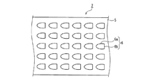
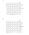
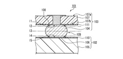
図1(a)は、本発明の実施の形態1における電子部品パッケージ3を用いた電子部品実装装置1の構成を示す断面概念図である。図1(b)は、図1(a)の一部を拡大した断面概念図である。これらの図において、同じ構成の要素には、同じ符号を付与し、符号の一部を省略している。図2Aは、本実施の形態におけるキャリア基板の下面8bの概念図である。図2Bは、本実施の形態における回路基板2の概念図である。図2Aおよび図2Bにおいて、図1(a)および図1(b)と同じ構成の要素には、同じ符号を付与し、符号の一部を省略している。
図7は、本発明の実施の形態2に係る半導体(電子部品)実装装置のキャリア基板8における外部接続用ランド31の構成を示す平面図である。本実施の形態に係る半導体実装装置は、実施の形態1の電子部品実装装置と外部接続用ランド31の構成が異なるだけであり、他の構成は実施の形態1の電子部品実装装置と同様である。本実施の形態の半導体実装装置において、実施の形態1の電子部品実装装置と同一の構成要素については、同一の符号を付して説明を省略する。
図10は、本発明の実施の形態3に係る電子部品実装装置41の構成を示す平面図である。電子部品実装装置41は、回路基板42に電子部品パッケージ43が実装された構成である。回路基板42は、エポキシ樹脂などの絶縁基板と、絶縁基板上に敷設された配線(図示せず)と、配線および回路基板42上に配置されたレジストとを有する。配線は、銅などで形成されている。また、配線の端部には、電子部品パッケージ43と接続するための回路基板側ランド(図10には図示せず)が形成されている。
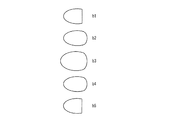
図15は、本発明の実施の形態4に係る電子部品実装装置の外部接続用ランド61が配置された領域の構成を示す平面図である。本実施の形態は、実施の形態3における外部接続用ランド57が楕円形の外部接続用ランド61に置き換わった構成であり、他の構成は実施の形態3と同様である。なお、回路基板側のレジスト51と回路基板側ランド53の形状および位置関係は、レジスト58と外部接続用ランド61の形状および位置関係と同じであるので、説明を省略する。また、本実施の形態において、実施の形態3と同一の構成要素については、同一の符号を付して説明を省略する。
2、42 回路基板
3、43 電子部品パッケージ
4、14、56 半田ボール
5、55 絶縁基板
6、53 回路基板側ランド
6a、10a 楕円弧部
6b、10b、33 直線部
7、15、51、58、58b レジスト
8 キャリア基板
8a キャリア基板の上面
8b キャリア基板の下面
9 接続配線
10、10c、10d、31、57、57b、61 外部接続用ランド
11 ビアホール
12 ICチップ
13 電極バンプ
16 接合部
21 半田ボール像
22 接合部分像
32 第1半田ボール
34 第2半田ボール
35〜37 外部接続用ランド
52、52b 開口部
54、54b 隙間
59 電子部品
Claims (7)
- 絶縁体からなるキャリア基板の一方の面にICチップが実装され、当該キャリア基板の他方の面に前記ICチップの外部接続用ランドが配置されるとともに、その外部接続用ランドに半田ボールが接合された電子部品パッケージであって、
前記外部接続用ランドにおける前記半田ボールが接合された接合可能部分の外形形状は、半円状の弧部と、前記弧部の両端を結ぶ直線部とからなることを特徴とする電子部品パッケージ。 - 前記キャリア基板の他方の面にレジストを備え、
前記外部接続用ランドにおける半田ボールの接合可能部分の外形形状は、前記レジストに形成された開口部の形状である請求項1記載の電子部品パッケージ。 - 絶縁基板と、
前記絶縁基板上に敷設された配線と、
その配線に接続された回路基板側ランドを備え、
前記回路基板側ランドに、ICチップを備えた電子部品パッケージの外部接続用ランドに接合された半田ボールが接合される回路基板であって、
前記回路基板側ランドにおける前記半田ボールの接合可能部分の外形形状は、半円状の弧部と、前記弧部の両端を結ぶ直線部とからなることを特徴とする回路基板。 - 前記回路基板側ランドにおける前記半田ボールの接合可能部分の外形形状は、回路基板に配置したレジストに形成された開口部の形状である請求項3記載の回路基板。
- 請求項1または2に記載の電子部品パッケージと、
請求項3または4に記載の回路基板とを備え、
前記電子部品パッケージの外部接続用ランドに接合された半田ボールが前記回路基板の回路基板側ランドに接続され、回路基板に電子部品パッケージが実装された電子部品実装装置。 - 請求項1または2に記載の電子部品パッケージにおけるキャリア基板の外部接続用ランドと半田ボールとの接合部の接合状態を検査する方法であって、
前記接合部にX線を照射し、前記接合部を透過したX線による表示画像において、前記半田ボールの外形を示す形状に直線部分が含まれる場合に、前記外部接続用ランドと半田ボールとの接合部が接合良好であると判断する電子部品パッケージの接合部の検査方法。 - 請求項5に記載の電子部品実装装置における半田ボールによる外部接続用ランドと回路基板側ランドとの接合部を検査する方法であって、
前記接合部にX線を照射し、前記接合部を透過したX線による表示画像において、前記外部接続用ランドの接合可能部分における半田ボールの外形を示す形状および前記回路基板側ランドの接合可能部分における半田ボールの外形を示す形状にそれぞれ直線部分が含まれる場合に、前記接合部が接合良好であると判断する電子部品実装装置の接合部の検査方法。
Priority Applications (1)
| Application Number | Priority Date | Filing Date | Title |
|---|---|---|---|
| JP2008110463A JP5331371B2 (ja) | 2007-04-24 | 2008-04-21 | 電子部品パッケージ、回路基板、電子部品実装装置、およびそれらの接合部の検査方法 |
Applications Claiming Priority (5)
| Application Number | Priority Date | Filing Date | Title |
|---|---|---|---|
| JP2007113721 | 2007-04-24 | ||
| JP2007113721 | 2007-04-24 | ||
| JP2008058263 | 2008-03-07 | ||
| JP2008058263 | 2008-03-07 | ||
| JP2008110463A JP5331371B2 (ja) | 2007-04-24 | 2008-04-21 | 電子部品パッケージ、回路基板、電子部品実装装置、およびそれらの接合部の検査方法 |
Publications (3)
| Publication Number | Publication Date |
|---|---|
| JP2009239239A JP2009239239A (ja) | 2009-10-15 |
| JP2009239239A5 JP2009239239A5 (ja) | 2011-05-12 |
| JP5331371B2 true JP5331371B2 (ja) | 2013-10-30 |
Family
ID=39886707
Family Applications (1)
| Application Number | Title | Priority Date | Filing Date |
|---|---|---|---|
| JP2008110463A Expired - Fee Related JP5331371B2 (ja) | 2007-04-24 | 2008-04-21 | 電子部品パッケージ、回路基板、電子部品実装装置、およびそれらの接合部の検査方法 |
Country Status (2)
| Country | Link |
|---|---|
| US (1) | US8233288B2 (ja) |
| JP (1) | JP5331371B2 (ja) |
Families Citing this family (4)
| Publication number | Priority date | Publication date | Assignee | Title |
|---|---|---|---|---|
| JP5473666B2 (ja) * | 2010-02-19 | 2014-04-16 | 三菱電機株式会社 | X線検査方法及びx線検査装置 |
| JP6468054B2 (ja) * | 2015-04-28 | 2019-02-13 | 富士通株式会社 | プリント基板及びシールド板金固定方法 |
| JP6436141B2 (ja) | 2016-09-20 | 2018-12-12 | オムロン株式会社 | X線検査装置およびその制御方法 |
| KR20180041811A (ko) | 2016-10-14 | 2018-04-25 | 삼성전자주식회사 | 반도체 소자 |
Family Cites Families (12)
| Publication number | Priority date | Publication date | Assignee | Title |
|---|---|---|---|---|
| JP2932964B2 (ja) | 1995-03-30 | 1999-08-09 | 松下電器産業株式会社 | チップキャリアとその実装体 |
| JPH10335796A (ja) | 1997-05-29 | 1998-12-18 | Canon Inc | 回路基板と電子回路装置、及びその製造方法、及びその接合部の検査方法 |
| JPH11297889A (ja) | 1998-04-16 | 1999-10-29 | Sony Corp | 半導体パッケージおよび実装基板、ならびにこれらを用いた実装方法 |
| US6518675B2 (en) * | 2000-12-29 | 2003-02-11 | Samsung Electronics Co., Ltd. | Wafer level package and method for manufacturing the same |
| JP3860000B2 (ja) * | 2001-09-07 | 2006-12-20 | Necエレクトロニクス株式会社 | 半導体装置およびその製造方法 |
| JP3857103B2 (ja) * | 2001-10-22 | 2006-12-13 | 京セラ株式会社 | 配線基板 |
| JP4341552B2 (ja) | 2002-05-17 | 2009-10-07 | 日本電気株式会社 | プリント配線板 |
| JP2004311535A (ja) * | 2003-04-03 | 2004-11-04 | Matsushita Electric Ind Co Ltd | チップサイズパッケージ半導体装置 |
| JP2006024858A (ja) | 2004-07-09 | 2006-01-26 | Audio Technica Corp | プリント配線板の製造方法およびプリント配線板 |
| JP2006041167A (ja) * | 2004-07-27 | 2006-02-09 | Matsushita Electric Ind Co Ltd | 半導体装置の検査方法および検査装置 |
| JP4910378B2 (ja) * | 2005-03-01 | 2012-04-04 | 株式会社デンソー | X線検査装置及びx線検査方法 |
| JP2007005452A (ja) | 2005-06-22 | 2007-01-11 | Renesas Technology Corp | 半導体装置 |
-
2008
- 2008-04-21 JP JP2008110463A patent/JP5331371B2/ja not_active Expired - Fee Related
- 2008-04-22 US US12/107,454 patent/US8233288B2/en active Active
Also Published As
| Publication number | Publication date |
|---|---|
| US20080266825A1 (en) | 2008-10-30 |
| JP2009239239A (ja) | 2009-10-15 |
| US8233288B2 (en) | 2012-07-31 |
Similar Documents
| Publication | Publication Date | Title |
|---|---|---|
| US6734557B2 (en) | Semiconductor device | |
| US20130119012A1 (en) | Interconnection element for electric circuits | |
| JP5107959B2 (ja) | 基板 | |
| JP5143211B2 (ja) | 半導体モジュール | |
| WO2012035688A1 (ja) | 半導体装置、半導体装置ユニット、および半導体装置の製造方法 | |
| KR100636364B1 (ko) | 플립칩 패키지의 솔더패드 접합방법 | |
| JP5331371B2 (ja) | 電子部品パッケージ、回路基板、電子部品実装装置、およびそれらの接合部の検査方法 | |
| JP2009239239A5 (ja) | ||
| JP3613167B2 (ja) | パッド電極の接続状態の検査方法 | |
| US8716868B2 (en) | Semiconductor module for stacking and stacked semiconductor module | |
| JP2022173486A (ja) | プリント回路板及び電子機器 | |
| JP3601714B2 (ja) | 半導体装置及び配線基板 | |
| JP5489860B2 (ja) | 積層型半導体モジュール | |
| JP2007266501A (ja) | 半導体装置の実装方法及び実装基板 | |
| JP4828139B2 (ja) | 半導体装置 | |
| JPH10335796A (ja) | 回路基板と電子回路装置、及びその製造方法、及びその接合部の検査方法 | |
| JP4191169B2 (ja) | 半導体装置及び実装体 | |
| JPH1074802A (ja) | ボールグリッドアレイパッケージの接続構造及びその接続検査方法 | |
| JP2019192789A (ja) | 配線基板、電子装置 | |
| JP4712426B2 (ja) | 半導体装置 | |
| WO2015033509A1 (ja) | プリント配線板およびそれを備えた半導体装置 | |
| JP2003017864A (ja) | 多層基板 | |
| JP2007005495A (ja) | プリント配線板及び半導体パッケージの実装方法 | |
| JP2009266994A (ja) | 半導体装置およびその実装構造 | |
| JP2005072211A (ja) | 電子部品とその製造方法及び電子装置 |
Legal Events
| Date | Code | Title | Description |
|---|---|---|---|
| A521 | Request for written amendment filed |
Free format text: JAPANESE INTERMEDIATE CODE: A523 Effective date: 20110329 |
|
| A621 | Written request for application examination |
Free format text: JAPANESE INTERMEDIATE CODE: A621 Effective date: 20110329 |
|
| A131 | Notification of reasons for refusal |
Free format text: JAPANESE INTERMEDIATE CODE: A131 Effective date: 20130618 |
|
| A521 | Request for written amendment filed |
Free format text: JAPANESE INTERMEDIATE CODE: A523 Effective date: 20130701 |
|
| TRDD | Decision of grant or rejection written | ||
| A01 | Written decision to grant a patent or to grant a registration (utility model) |
Free format text: JAPANESE INTERMEDIATE CODE: A01 Effective date: 20130723 |
|
| A61 | First payment of annual fees (during grant procedure) |
Free format text: JAPANESE INTERMEDIATE CODE: A61 Effective date: 20130729 |
|
| R150 | Certificate of patent or registration of utility model |
Ref document number: 5331371 Country of ref document: JP Free format text: JAPANESE INTERMEDIATE CODE: R150 Free format text: JAPANESE INTERMEDIATE CODE: R150 |
|
| LAPS | Cancellation because of no payment of annual fees |