JP5319084B2 - 半導体装置 - Google Patents
半導体装置 Download PDFInfo
- Publication number
- JP5319084B2 JP5319084B2 JP2007160882A JP2007160882A JP5319084B2 JP 5319084 B2 JP5319084 B2 JP 5319084B2 JP 2007160882 A JP2007160882 A JP 2007160882A JP 2007160882 A JP2007160882 A JP 2007160882A JP 5319084 B2 JP5319084 B2 JP 5319084B2
- Authority
- JP
- Japan
- Prior art keywords
- semiconductor
- semiconductor layer
- main surface
- layer
- diode
- Prior art date
- Legal status (The legal status is an assumption and is not a legal conclusion. Google has not performed a legal analysis and makes no representation as to the accuracy of the status listed.)
- Expired - Fee Related
Links
Images


Classifications
-
- H—ELECTRICITY
- H10—SEMICONDUCTOR DEVICES; ELECTRIC SOLID-STATE DEVICES NOT OTHERWISE PROVIDED FOR
- H10D—INORGANIC ELECTRIC SEMICONDUCTOR DEVICES
- H10D84/00—Integrated devices formed in or on semiconductor substrates that comprise only semiconducting layers, e.g. on Si wafers or on GaAs-on-Si wafers
- H10D84/01—Manufacture or treatment
-
- H—ELECTRICITY
- H10—SEMICONDUCTOR DEVICES; ELECTRIC SOLID-STATE DEVICES NOT OTHERWISE PROVIDED FOR
- H10D—INORGANIC ELECTRIC SEMICONDUCTOR DEVICES
- H10D30/00—Field-effect transistors [FET]
- H10D30/40—FETs having zero-dimensional [0D], one-dimensional [1D] or two-dimensional [2D] charge carrier gas channels
- H10D30/47—FETs having zero-dimensional [0D], one-dimensional [1D] or two-dimensional [2D] charge carrier gas channels having two-dimensional [2D] charge carrier gas channels, e.g. nanoribbon FETs or high electron mobility transistors [HEMT]
- H10D30/471—High electron mobility transistors [HEMT] or high hole mobility transistors [HHMT]
- H10D30/475—High electron mobility transistors [HEMT] or high hole mobility transistors [HHMT] having wider bandgap layer formed on top of lower bandgap active layer, e.g. undoped barrier HEMTs such as i-AlGaN/GaN HEMTs
- H10D30/4755—High electron mobility transistors [HEMT] or high hole mobility transistors [HHMT] having wider bandgap layer formed on top of lower bandgap active layer, e.g. undoped barrier HEMTs such as i-AlGaN/GaN HEMTs having wide bandgap charge-carrier supplying layers, e.g. modulation doped HEMTs such as n-AlGaAs/GaAs HEMTs
-
- H—ELECTRICITY
- H10—SEMICONDUCTOR DEVICES; ELECTRIC SOLID-STATE DEVICES NOT OTHERWISE PROVIDED FOR
- H10D—INORGANIC ELECTRIC SEMICONDUCTOR DEVICES
- H10D8/00—Diodes
-
- H—ELECTRICITY
- H10—SEMICONDUCTOR DEVICES; ELECTRIC SOLID-STATE DEVICES NOT OTHERWISE PROVIDED FOR
- H10D—INORGANIC ELECTRIC SEMICONDUCTOR DEVICES
- H10D84/00—Integrated devices formed in or on semiconductor substrates that comprise only semiconducting layers, e.g. on Si wafers or on GaAs-on-Si wafers
- H10D84/01—Manufacture or treatment
- H10D84/02—Manufacture or treatment characterised by using material-based technologies
- H10D84/08—Manufacture or treatment characterised by using material-based technologies using combinations of technologies, e.g. using both Si and SiC technologies or using both Si and Group III-V technologies
-
- H—ELECTRICITY
- H10—SEMICONDUCTOR DEVICES; ELECTRIC SOLID-STATE DEVICES NOT OTHERWISE PROVIDED FOR
- H10D—INORGANIC ELECTRIC SEMICONDUCTOR DEVICES
- H10D84/00—Integrated devices formed in or on semiconductor substrates that comprise only semiconducting layers, e.g. on Si wafers or on GaAs-on-Si wafers
- H10D84/80—Integrated devices formed in or on semiconductor substrates that comprise only semiconducting layers, e.g. on Si wafers or on GaAs-on-Si wafers characterised by the integration of at least one component covered by groups H10D12/00 or H10D30/00, e.g. integration of IGFETs
- H10D84/811—Combinations of field-effect devices and one or more diodes, capacitors or resistors
-
- H—ELECTRICITY
- H10—SEMICONDUCTOR DEVICES; ELECTRIC SOLID-STATE DEVICES NOT OTHERWISE PROVIDED FOR
- H10D—INORGANIC ELECTRIC SEMICONDUCTOR DEVICES
- H10D88/00—Three-dimensional [3D] integrated devices
-
- H—ELECTRICITY
- H10—SEMICONDUCTOR DEVICES; ELECTRIC SOLID-STATE DEVICES NOT OTHERWISE PROVIDED FOR
- H10D—INORGANIC ELECTRIC SEMICONDUCTOR DEVICES
- H10D62/00—Semiconductor bodies, or regions thereof, of devices having potential barriers
- H10D62/80—Semiconductor bodies, or regions thereof, of devices having potential barriers characterised by the materials
- H10D62/85—Semiconductor bodies, or regions thereof, of devices having potential barriers characterised by the materials being Group III-V materials, e.g. GaAs
- H10D62/8503—Nitride Group III-V materials, e.g. AlN or GaN
-
- H—ELECTRICITY
- H10—SEMICONDUCTOR DEVICES; ELECTRIC SOLID-STATE DEVICES NOT OTHERWISE PROVIDED FOR
- H10D—INORGANIC ELECTRIC SEMICONDUCTOR DEVICES
- H10D64/00—Electrodes of devices having potential barriers
- H10D64/20—Electrodes characterised by their shapes, relative sizes or dispositions
- H10D64/23—Electrodes carrying the current to be rectified, amplified, oscillated or switched, e.g. sources, drains, anodes or cathodes
- H10D64/251—Source or drain electrodes for field-effect devices
- H10D64/256—Source or drain electrodes for field-effect devices for lateral devices wherein the source or drain electrodes are recessed in semiconductor bodies
-
- H—ELECTRICITY
- H10—SEMICONDUCTOR DEVICES; ELECTRIC SOLID-STATE DEVICES NOT OTHERWISE PROVIDED FOR
- H10W—GENERIC PACKAGES, INTERCONNECTIONS, CONNECTORS OR OTHER CONSTRUCTIONAL DETAILS OF DEVICES COVERED BY CLASS H10
- H10W72/00—Interconnections or connectors in packages
- H10W72/50—Bond wires
- H10W72/541—Dispositions of bond wires
- H10W72/547—Dispositions of multiple bond wires
- H10W72/5475—Dispositions of multiple bond wires multiple bond wires connected to common bond pads at both ends of the wires
-
- H—ELECTRICITY
- H10—SEMICONDUCTOR DEVICES; ELECTRIC SOLID-STATE DEVICES NOT OTHERWISE PROVIDED FOR
- H10W—GENERIC PACKAGES, INTERCONNECTIONS, CONNECTORS OR OTHER CONSTRUCTIONAL DETAILS OF DEVICES COVERED BY CLASS H10
- H10W72/00—Interconnections or connectors in packages
- H10W72/90—Bond pads, in general
- H10W72/921—Structures or relative sizes of bond pads
- H10W72/926—Multiple bond pads having different sizes
-
- H—ELECTRICITY
- H10—SEMICONDUCTOR DEVICES; ELECTRIC SOLID-STATE DEVICES NOT OTHERWISE PROVIDED FOR
- H10W—GENERIC PACKAGES, INTERCONNECTIONS, CONNECTORS OR OTHER CONSTRUCTIONAL DETAILS OF DEVICES COVERED BY CLASS H10
- H10W90/00—Package configurations
- H10W90/701—Package configurations characterised by the relative positions of pads or connectors relative to package parts
- H10W90/751—Package configurations characterised by the relative positions of pads or connectors relative to package parts of bond wires
- H10W90/756—Package configurations characterised by the relative positions of pads or connectors relative to package parts of bond wires between a chip and a stacked lead frame, conducting package substrate or heat sink
Landscapes
- Junction Field-Effect Transistors (AREA)
- Electrodes Of Semiconductors (AREA)
Description
本実施の形態1では、高電子移動度トランジスタを備えた半導体装置を、電力変換装置のスイッチング素子として適用する実施態様について説明する。
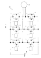
まず、図1を用いて本実施の形態1の電力変換装置の回路構成について説明する。図1は本実施の形態1の電力変換装置の回路図である。
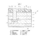
次に、図2を用いて本実施の形態1の半導体装置の構造について説明する。
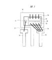
次に図3を用いて図2に示す半導体チップ30を電力変換装置のスイッチング素子として実装した半導体パッケージの構造例について説明する。図3は図1の半導体チップ30のパッケージ構造例を示す平面図である。
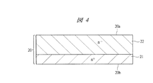
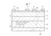
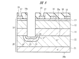
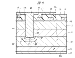
次に、図4〜図9を用いて図2に示す半導体装置の製造方法を説明する。
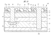
次に、図10を用いて本実施の形態2の半導体装置について説明する。図10は本実施の形態2の半導体装置を構成する半導体チップ40の要部断面図である。
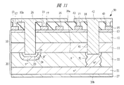
次に、図11を用いて本実施の形態3の半導体装置について説明する。図11は本実施の形態3の半導体装置を構成する半導体チップ50の要部断面図である。
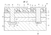
次に、図12を用いて本実施の形態4の半導体装置について説明する。図12は本実施の形態4の半導体装置を構成する半導体チップ60の要部断面図である。
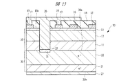
次に、図13を用いて本実施の形態5の半導体装置について説明する。図13は本実施の形態5の半導体チップ70の構造を示す断面図である。
次に、図14を用いて本実施の形態6の半導体装置について説明する。図14は本実施の形態6の半導体装置を構成する半導体チップ80の要部断面図である。
2 ダイオード
3 スイッチング素子
4 ゲートドライバ
10 化合物半導体層(第2基板)
10a 主面(第3主面)
11 バッファ層(第1化合物半導体層)
12 チャネル層(第2化合物半導体層)
13 電子供給層(第3化合物半導体層)
15 ドレイン電極
16 ゲート電極
17 ソース電極
18 絶縁層
19 コンタクトホール
20 半導体基板(第1基板)
20a 主面(第1主面)
20b 主面(第2主面)
21 n+層(第1半導体層、カソード領域)
22 n−層(第2半導体層、カソード領域)
23 p+領域(アノード領域)
24 p−領域(アノード領域)
25 ビアホール
26 アノード電極
27 カソード電極
30、40、50、60、70、80 半導体チップ(半導体装置)
31 ゲートパッド
32 ソースパッド
33 ドレインパッド
34 ゲート端子
35 ソース端子
36 ドレイン端子
37、38、39 ボンディングワイヤ
41 ビアホール
42 導電体
43 コンタクトホール
51 n+領域(第3半導体領域)
61 カソード電極
71 ショットキーバリア金属
81 n+層(第1半導体層、カソード領域)
82 n−層(第2半導体層、カソード領域)
100 電力変換装置
101 直流電源
102 モータ
Claims (9)
- 同一の半導体チップ内に高電子移動度トランジスタとダイオードとを有し、
前記半導体チップは、
厚さ方向に沿って互いに反対側に位置する第1主面および第2主面を有する半導体基板と、
前記半導体基板上に形成された化合物半導体層とを有しており、
前記高電子移動度トランジスタは、
前記化合物半導体層と、前記化合物半導体層の主面上に形成されたドレイン電極、ゲート電極およびソース電極とを有しており、
前記ダイオードは、
前記半導体基板に形成されたカソード領域と、
前記カソード領域に接するように前記半導体基板の前記第1主面側に形成されたアノード領域と、
前記化合物半導体層の主面上に形成されたアノード電極とを有しており、
前記アノード電極は、前記化合物半導体層の主面から前記半導体基板の前記第1主面の前記アノード領域に達する孔に埋め込まれた導電体を通じて前記アノード領域に電気的に接続されており、
前記高電子移動度トランジスタの前記ソース電極と、前記ダイオードの前記アノード領域とは電気的に接続されており、
前記高電子移動度トランジスタの前記ソース電極と、前記ダイオードの前記アノード領域とは前記アノード電極を構成する前記導電体によって電気的に接続されており、
前記化合物半導体層の主面上には、前記ドレイン電極、前記ゲート電極および前記ソース電極が所定の間隔を持って順に配置され、
前記アノード電極は、前記化合物半導体層の主面上方において、前記ソース電極側から前記ゲート電極と前記ドレイン電極との間まで前記化合物半導体層の主面に沿って延在するように配置されていることを特徴とする半導体装置。 - 請求項1に記載の半導体装置において、
前記ダイオードのカソード電極は、前記高電子移動度トランジスタの前記ドレイン電極と、前記半導体チップ内で電気的に接続されていることを特徴とする半導体装置。 - 請求項2に記載の半導体装置において、
前記半導体基板は、
前記第2主面から順に積層される第1導電型の第1半導体層、および第2半導体層とを備え、
前記第1半導体層は、第1不純物濃度であり、
前記第2半導体層は、前記第1不純物濃度よりも低い第2不純物濃度であり、
前記ダイオードの前記カソード電極は、前記化合物半導体層の主面から前記半導体基板の前記第1半導体層に達する孔に埋め込まれた前記導電体を通じて前記ドレイン電極に電気的に接続されていることを特徴とする半導体装置。 - 請求項2に記載の半導体装置において、
前記半導体基板は、
前記第2主面から順に積層される第1導電型の第1半導体層、および第2半導体層とを備え、
前記第1半導体層は、第1不純物濃度であり、
前記第2半導体層は、前記第1不純物濃度よりも低い第2不純物濃度であり、
前記第2半導体層には、前記第1主面から前記第1半導体層との接触面まで達するように延在する第3半導体領域を備え、
前記ダイオードの前記カソード電極は、前記化合物半導体層の主面から前記半導体基板の前記第3半導体領域に達する孔に埋め込まれた前記導電体を通じて前記ドレイン電極に電気的に接続されていることを特徴とする半導体装置。 - 請求項1に記載の半導体装置において、
前記半導体基板は、
前記第2主面から順に積層される第1導電型の第1半導体層、および第2半導体層とを備え、
前記第1半導体層は、第1不純物濃度であり、
前記第2半導体層は、前記第1不純物濃度よりも低い第2不純物濃度であり、
前記ダイオードは、前記半導体基板の前記第2主面にカソード電極を備えていることを特徴とする半導体装置。 - 請求項1に記載の半導体装置において、
前記半導体基板を構成する半導体材料はシリコンであることを特徴とする半導体装置。 - 請求項3に記載の半導体装置において、
前記ダイオードの前記アノード領域は、前記第1導電型と反対導電型の半導体領域であることを特徴とする半導体装置。 - 請求項1に記載の半導体装置において、
前記半導体基板は、
前記第2主面から順に積層される第1導電型の第1半導体層、および第2半導体層とを備え、
前記第1半導体層は、第1不純物濃度であり、
前記第2半導体層は、前記第1不純物濃度よりも低い第2不純物濃度であり、
前記ダイオードの前記アノード領域は、ショットキーバリア金属であることを特徴とする半導体装置。 - 請求項8に記載の半導体装置において、
前記半導体基板を構成する半導体材料はシリコンカーバイドであることを特徴とする半導体装置。
Priority Applications (2)
| Application Number | Priority Date | Filing Date | Title |
|---|---|---|---|
| JP2007160882A JP5319084B2 (ja) | 2007-06-19 | 2007-06-19 | 半導体装置 |
| US12/141,978 US7838907B2 (en) | 2007-06-19 | 2008-06-19 | Semiconductor device and power conversion device using the same |
Applications Claiming Priority (1)
| Application Number | Priority Date | Filing Date | Title |
|---|---|---|---|
| JP2007160882A JP5319084B2 (ja) | 2007-06-19 | 2007-06-19 | 半導体装置 |
Publications (2)
| Publication Number | Publication Date |
|---|---|
| JP2009004398A JP2009004398A (ja) | 2009-01-08 |
| JP5319084B2 true JP5319084B2 (ja) | 2013-10-16 |
Family
ID=40135551
Family Applications (1)
| Application Number | Title | Priority Date | Filing Date |
|---|---|---|---|
| JP2007160882A Expired - Fee Related JP5319084B2 (ja) | 2007-06-19 | 2007-06-19 | 半導体装置 |
Country Status (2)
| Country | Link |
|---|---|
| US (1) | US7838907B2 (ja) |
| JP (1) | JP5319084B2 (ja) |
Cited By (1)
| Publication number | Priority date | Publication date | Assignee | Title |
|---|---|---|---|---|
| US10158012B1 (en) | 2017-06-16 | 2018-12-18 | Kabushiki Kaisha Toshiba | Semiconductor device |
Families Citing this family (71)
| Publication number | Priority date | Publication date | Assignee | Title |
|---|---|---|---|---|
| US8017978B2 (en) * | 2006-03-10 | 2011-09-13 | International Rectifier Corporation | Hybrid semiconductor device |
| JP4478175B2 (ja) | 2007-06-26 | 2010-06-09 | 株式会社東芝 | 半導体装置 |
| JP5433214B2 (ja) * | 2007-12-07 | 2014-03-05 | パナソニック株式会社 | モータ駆動回路 |
| JP2009164158A (ja) * | 2007-12-28 | 2009-07-23 | Panasonic Corp | 半導体装置及びその製造方法 |
| JP5320774B2 (ja) * | 2008-03-03 | 2013-10-23 | 三菱電機株式会社 | 半導体装置 |
| JP5524462B2 (ja) * | 2008-08-06 | 2014-06-18 | シャープ株式会社 | 半導体装置 |
| US20100207164A1 (en) * | 2008-08-22 | 2010-08-19 | Daisuke Shibata | Field effect transistor |
| CN202721890U (zh) * | 2009-02-13 | 2013-02-06 | 许廷格电子两合公司 | 用于等离子体供给装置的模块和等离子体供给装置 |
| DE102009018054B4 (de) * | 2009-04-21 | 2018-11-29 | Infineon Technologies Austria Ag | Lateraler HEMT und Verfahren zur Herstellung eines lateralen HEMT |
| US7915645B2 (en) * | 2009-05-28 | 2011-03-29 | International Rectifier Corporation | Monolithic vertically integrated composite group III-V and group IV semiconductor device and method for fabricating same |
| US20110147796A1 (en) * | 2009-12-17 | 2011-06-23 | Infineon Technologies Austria Ag | Semiconductor device with metal carrier and manufacturing method |
| US9219058B2 (en) * | 2010-03-01 | 2015-12-22 | Infineon Technologies Americas Corp. | Efficient high voltage switching circuits and monolithic integration of same |
| US8981380B2 (en) * | 2010-03-01 | 2015-03-17 | International Rectifier Corporation | Monolithic integration of silicon and group III-V devices |
| JP5056883B2 (ja) | 2010-03-26 | 2012-10-24 | サンケン電気株式会社 | 半導体装置 |
| JP5672756B2 (ja) * | 2010-04-16 | 2015-02-18 | サンケン電気株式会社 | 半導体装置 |
| WO2011161791A1 (ja) | 2010-06-24 | 2011-12-29 | 富士通株式会社 | 半導体装置 |
| WO2012008027A1 (ja) * | 2010-07-14 | 2012-01-19 | 富士通株式会社 | 化合物半導体装置及びその製造方法 |
| JP5872766B2 (ja) * | 2010-12-10 | 2016-03-01 | ローム株式会社 | 半導体装置および半導体パッケージ |
| KR20130126948A (ko) * | 2010-12-15 | 2013-11-21 | 이피션트 파워 컨버젼 코퍼레이션 | 후면 격리를 갖는 반도체 소자 |
| WO2012114393A1 (ja) * | 2011-02-23 | 2012-08-30 | パナソニック株式会社 | 窒化物半導体装置 |
| JP5866773B2 (ja) * | 2011-02-25 | 2016-02-17 | 富士通株式会社 | 化合物半導体装置及びその製造方法 |
| JP5692357B2 (ja) | 2011-03-18 | 2015-04-01 | 富士通株式会社 | 化合物半導体装置及びその製造方法 |
| US9362905B2 (en) * | 2011-03-21 | 2016-06-07 | Infineon Technologies Americas Corp. | Composite semiconductor device with turn-on prevention control |
| ITTO20110603A1 (it) * | 2011-07-08 | 2013-01-09 | St Microelectronics Srl | Dispositivo elettronico basato su un composto di gallio su un substrato di silicio, e relativo metodo di fabbricazione |
| US9087812B2 (en) * | 2011-07-15 | 2015-07-21 | International Rectifier Corporation | Composite semiconductor device with integrated diode |
| US9281388B2 (en) * | 2011-07-15 | 2016-03-08 | Infineon Technologies Americas Corp. | Composite semiconductor device with a SOI substrate having an integrated diode |
| JP5896667B2 (ja) * | 2011-09-26 | 2016-03-30 | トランスフォーム・ジャパン株式会社 | 化合物半導体装置及びその製造方法 |
| US20130087803A1 (en) * | 2011-10-06 | 2013-04-11 | Epowersoft, Inc. | Monolithically integrated hemt and schottky diode |
| US9887139B2 (en) | 2011-12-28 | 2018-02-06 | Infineon Technologies Austria Ag | Integrated heterojunction semiconductor device and method for producing an integrated heterojunction semiconductor device |
| JP2013153027A (ja) * | 2012-01-24 | 2013-08-08 | Fujitsu Ltd | 半導体装置及び電源装置 |
| US8872235B2 (en) * | 2012-02-23 | 2014-10-28 | Infineon Technologies Austria Ag | Integrated Schottky diode for HEMTs |
| US9165839B2 (en) * | 2012-03-13 | 2015-10-20 | Taiwan Semiconductor Manufacturing Company, Ltd. | Plasma protection diode for a HEMT device |
| JP5659182B2 (ja) | 2012-03-23 | 2015-01-28 | 株式会社東芝 | 窒化物半導体素子 |
| JP5696083B2 (ja) | 2012-03-26 | 2015-04-08 | 株式会社東芝 | 窒化物半導体素子及びその製造方法 |
| JP2014036115A (ja) * | 2012-08-08 | 2014-02-24 | Renesas Electronics Corp | 半導体装置 |
| JP2014056938A (ja) * | 2012-09-12 | 2014-03-27 | Fujitsu Semiconductor Ltd | 半導体装置及びその製造方法 |
| JP6134119B2 (ja) * | 2012-10-05 | 2017-05-24 | ルネサスエレクトロニクス株式会社 | 半導体装置 |
| US9093462B2 (en) * | 2013-05-06 | 2015-07-28 | Qualcomm Incorporated | Electrostatic discharge diode |
| JP6107435B2 (ja) | 2013-06-04 | 2017-04-05 | 三菱電機株式会社 | 半導体装置及びその製造方法 |
| WO2015008444A1 (ja) * | 2013-07-16 | 2015-01-22 | パナソニックIpマネジメント株式会社 | 半導体装置 |
| JP6143598B2 (ja) * | 2013-08-01 | 2017-06-07 | 株式会社東芝 | 半導体装置 |
| KR101758082B1 (ko) * | 2013-12-30 | 2017-07-17 | 한국전자통신연구원 | 질화물 반도체 소자의 제조 방법 |
| US10290566B2 (en) * | 2014-09-23 | 2019-05-14 | Infineon Technologies Austria Ag | Electronic component |
| JP6319028B2 (ja) * | 2014-10-03 | 2018-05-09 | 三菱電機株式会社 | 半導体装置 |
| US9356017B1 (en) | 2015-02-05 | 2016-05-31 | Infineon Technologies Austria Ag | Switch circuit and semiconductor device |
| JP6478395B2 (ja) * | 2015-03-06 | 2019-03-06 | 住友電工デバイス・イノベーション株式会社 | 半導体装置 |
| ITUB20155862A1 (it) * | 2015-11-24 | 2017-05-24 | St Microelectronics Srl | Transistore di tipo normalmente spento con ridotta resistenza in stato acceso e relativo metodo di fabbricazione |
| US11430882B2 (en) | 2016-06-24 | 2022-08-30 | Wolfspeed, Inc. | Gallium nitride high-electron mobility transistors with p-type layers and process for making the same |
| US12484244B2 (en) | 2016-06-24 | 2025-11-25 | Wolfspeed, Inc. | Group III-nitride high-electron mobility transistors with gate connected buried p-type layers and process for making the same |
| US10892356B2 (en) | 2016-06-24 | 2021-01-12 | Cree, Inc. | Group III-nitride high-electron mobility transistors with buried p-type layers and process for making the same |
| US9881862B1 (en) | 2016-09-20 | 2018-01-30 | Infineon Technologies Austria Ag | Top side cooling for GaN power device |
| US10128228B1 (en) | 2017-06-22 | 2018-11-13 | Infineon Technologies Americas Corp. | Type III-V semiconductor device with integrated diode |
| CN111213241B (zh) * | 2018-06-30 | 2023-09-22 | 魏进 | 半导体器件、半导体设备及其制造方法 |
| EP3918636A4 (en) * | 2019-01-28 | 2023-03-08 | Wolfspeed, Inc. | Group iii-nitride high-electron mobility transistors with buried p-type layers and process for making the same |
| CN113826206B (zh) * | 2019-03-21 | 2025-10-21 | 创世舫科技有限公司 | Iii-氮化物器件的集成设计 |
| CN112331718B (zh) * | 2019-08-05 | 2022-02-22 | 苏州捷芯威半导体有限公司 | 一种半导体器件及其制备方法 |
| CN219040486U (zh) * | 2020-01-16 | 2023-05-16 | 华为技术有限公司 | 一种氮化物半导体晶体管及电子设备 |
| CN111312711A (zh) * | 2020-02-25 | 2020-06-19 | 英诺赛科(珠海)科技有限公司 | 半导体器件及其制造方法 |
| CN111312712A (zh) * | 2020-02-25 | 2020-06-19 | 英诺赛科(珠海)科技有限公司 | 半导体器件及其制造方法 |
| DE112021004164T5 (de) * | 2020-09-08 | 2023-06-01 | Rohm Co., Ltd. | Halbleiterbauelement |
| US20240405118A1 (en) * | 2021-02-01 | 2024-12-05 | Sony Semiconductor Solutions Corporation | Semiconductor device, semiconductor module, and electronic apparatus |
| US12557322B2 (en) | 2021-05-17 | 2026-02-17 | Wolfspeed, Inc. | Group III-nitride transistors with back barrier structures and buried p-type layers and methods thereof |
| US11929428B2 (en) | 2021-05-17 | 2024-03-12 | Wolfspeed, Inc. | Circuits and group III-nitride high-electron mobility transistors with buried p-type layers improving overload recovery and process for implementing the same |
| US12402346B2 (en) | 2021-05-17 | 2025-08-26 | Wolfspeed, Inc. | Circuits and group III-nitride transistors with buried p-layers and controlled gate voltages and methods thereof |
| WO2023106087A1 (ja) | 2021-12-09 | 2023-06-15 | 国立研究開発法人産業技術総合研究所 | 半導体装置 |
| CN115332334A (zh) * | 2022-08-26 | 2022-11-11 | 电子科技大学 | 具有反向续流能力的集成二极管的GaN HEMT纵向器件 |
| CN115832040A (zh) * | 2022-11-11 | 2023-03-21 | 深圳天狼芯半导体有限公司 | 碳化硅基氮化镓器件及其制备方法 |
| CN115799330A (zh) * | 2022-11-11 | 2023-03-14 | 深圳天狼芯半导体有限公司 | 耐高压hemt器件及其制备方法 |
| US20240213239A1 (en) * | 2022-12-21 | 2024-06-27 | Analog Devices, Inc. | High-electron-mobility transistor device with integrated p-n layer |
| US20240395805A1 (en) * | 2023-05-26 | 2024-11-28 | Cambridge Gan Devices Limited | Power semiconductor device comprising a silicon substrate |
| US20240395804A1 (en) * | 2023-05-26 | 2024-11-28 | Cambridge Gan Devices Limited | Power semiconductor device comprising a wide bandgap substrate |
Family Cites Families (8)
| Publication number | Priority date | Publication date | Assignee | Title |
|---|---|---|---|---|
| SE515158C2 (sv) * | 1999-02-10 | 2001-06-18 | Ericsson Telefon Ab L M | Halvledaranordning med jordanslutning via en ej genomgående plugg |
| JP3317347B2 (ja) * | 1999-09-02 | 2002-08-26 | 日本電気株式会社 | ダイオードを備えた半導体装置およびその製造方法 |
| WO2002075780A2 (en) * | 2001-03-21 | 2002-09-26 | Koninklijke Philips Electronics N.V. | Electronic device having dielectric material of high dielectric constant |
| JP2006086398A (ja) * | 2004-09-17 | 2006-03-30 | Matsushita Electric Ind Co Ltd | 半導体装置及びその製造方法 |
| US7285807B2 (en) * | 2005-08-25 | 2007-10-23 | Coldwatt, Inc. | Semiconductor device having substrate-driven field-effect transistor and Schottky diode and method of forming the same |
| JP5052807B2 (ja) * | 2006-03-29 | 2012-10-17 | 古河電気工業株式会社 | 半導体装置及び電力変換装置 |
| JP2007273640A (ja) * | 2006-03-30 | 2007-10-18 | Sanken Electric Co Ltd | 半導体装置 |
| US7820519B2 (en) * | 2006-11-03 | 2010-10-26 | Freescale Semiconductor, Inc. | Process of forming an electronic device including a conductive structure extending through a buried insulating layer |
-
2007
- 2007-06-19 JP JP2007160882A patent/JP5319084B2/ja not_active Expired - Fee Related
-
2008
- 2008-06-19 US US12/141,978 patent/US7838907B2/en active Active
Cited By (1)
| Publication number | Priority date | Publication date | Assignee | Title |
|---|---|---|---|---|
| US10158012B1 (en) | 2017-06-16 | 2018-12-18 | Kabushiki Kaisha Toshiba | Semiconductor device |
Also Published As
| Publication number | Publication date |
|---|---|
| US7838907B2 (en) | 2010-11-23 |
| JP2009004398A (ja) | 2009-01-08 |
| US20080315257A1 (en) | 2008-12-25 |
Similar Documents
| Publication | Publication Date | Title |
|---|---|---|
| JP5319084B2 (ja) | 半導体装置 | |
| US10692861B2 (en) | Method of manufacturing a semiconductor device | |
| US12051662B2 (en) | Electronic component and semiconductor device | |
| JP4815885B2 (ja) | 半導体装置の制御方法 | |
| US9356017B1 (en) | Switch circuit and semiconductor device | |
| US8941117B2 (en) | Monolithically integrated vertical JFET and Schottky diode | |
| US9324645B2 (en) | Method and system for co-packaging vertical gallium nitride power devices | |
| US9324809B2 (en) | Method and system for interleaved boost converter with co-packaged gallium nitride power devices | |
| US9231056B2 (en) | Semiconductor device and fabrication method therefor, and power supply apparatus | |
| CN110431669B (zh) | 半导体装置以及电力变换装置 | |
| US8937317B2 (en) | Method and system for co-packaging gallium nitride electronics | |
| KR20160110011A (ko) | 반도체 장치 및 반도체 패키지 | |
| US10199347B2 (en) | Semiconductor device | |
| US20240063216A1 (en) | Semiconductor device and electronic device | |
| CN121003028A (zh) | 半导体装置以及电力转换装置 | |
| JP4876418B2 (ja) | 半導体装置 |
Legal Events
| Date | Code | Title | Description |
|---|---|---|---|
| A621 | Written request for application examination |
Free format text: JAPANESE INTERMEDIATE CODE: A621 Effective date: 20100209 |
|
| A711 | Notification of change in applicant |
Free format text: JAPANESE INTERMEDIATE CODE: A712 Effective date: 20100528 |
|
| A131 | Notification of reasons for refusal |
Free format text: JAPANESE INTERMEDIATE CODE: A131 Effective date: 20121218 |
|
| A521 | Request for written amendment filed |
Free format text: JAPANESE INTERMEDIATE CODE: A523 Effective date: 20130215 |
|
| TRDD | Decision of grant or rejection written | ||
| A01 | Written decision to grant a patent or to grant a registration (utility model) |
Free format text: JAPANESE INTERMEDIATE CODE: A01 Effective date: 20130618 |
|
| A61 | First payment of annual fees (during grant procedure) |
Free format text: JAPANESE INTERMEDIATE CODE: A61 Effective date: 20130711 |
|
| R150 | Certificate of patent or registration of utility model |
Ref document number: 5319084 Country of ref document: JP Free format text: JAPANESE INTERMEDIATE CODE: R150 Free format text: JAPANESE INTERMEDIATE CODE: R150 |
|
| S531 | Written request for registration of change of domicile |
Free format text: JAPANESE INTERMEDIATE CODE: R313531 |
|
| R350 | Written notification of registration of transfer |
Free format text: JAPANESE INTERMEDIATE CODE: R350 |
|
| LAPS | Cancellation because of no payment of annual fees |