JP5257955B2 - 可変利得をもつアナログ−デジタル変換器とその方法 - Google Patents
可変利得をもつアナログ−デジタル変換器とその方法 Download PDFInfo
- Publication number
- JP5257955B2 JP5257955B2 JP2010545045A JP2010545045A JP5257955B2 JP 5257955 B2 JP5257955 B2 JP 5257955B2 JP 2010545045 A JP2010545045 A JP 2010545045A JP 2010545045 A JP2010545045 A JP 2010545045A JP 5257955 B2 JP5257955 B2 JP 5257955B2
- Authority
- JP
- Japan
- Prior art keywords
- terminal
- capacitor
- amplifier
- input
- analog signal
- Prior art date
- Legal status (The legal status is an assumption and is not a legal conclusion. Google has not performed a legal analysis and makes no representation as to the accuracy of the status listed.)
- Expired - Fee Related
Links
Images


Classifications
-
- H—ELECTRICITY
- H03—ELECTRONIC CIRCUITRY
- H03M—CODING; DECODING; CODE CONVERSION IN GENERAL
- H03M1/00—Analogue/digital conversion; Digital/analogue conversion
- H03M1/12—Analogue/digital converters
- H03M1/18—Automatic control for modifying the range of signals the converter can handle, e.g. gain ranging
- H03M1/186—Automatic control for modifying the range of signals the converter can handle, e.g. gain ranging in feedforward mode, i.e. by determining the range to be selected directly from the input signal
-
- H—ELECTRICITY
- H03—ELECTRONIC CIRCUITRY
- H03M—CODING; DECODING; CODE CONVERSION IN GENERAL
- H03M1/00—Analogue/digital conversion; Digital/analogue conversion
- H03M1/06—Continuously compensating for, or preventing, undesired influence of physical parameters
- H03M1/0617—Continuously compensating for, or preventing, undesired influence of physical parameters characterised by the use of methods or means not specific to a particular type of detrimental influence
- H03M1/0675—Continuously compensating for, or preventing, undesired influence of physical parameters characterised by the use of methods or means not specific to a particular type of detrimental influence using redundancy
- H03M1/0678—Continuously compensating for, or preventing, undesired influence of physical parameters characterised by the use of methods or means not specific to a particular type of detrimental influence using redundancy using additional components or elements, e.g. dummy components
- H03M1/068—Continuously compensating for, or preventing, undesired influence of physical parameters characterised by the use of methods or means not specific to a particular type of detrimental influence using redundancy using additional components or elements, e.g. dummy components the original and additional components or elements being complementary to each other, e.g. CMOS
- H03M1/0682—Continuously compensating for, or preventing, undesired influence of physical parameters characterised by the use of methods or means not specific to a particular type of detrimental influence using redundancy using additional components or elements, e.g. dummy components the original and additional components or elements being complementary to each other, e.g. CMOS using a differential network structure, i.e. symmetrical with respect to ground
-
- H—ELECTRICITY
- H03—ELECTRONIC CIRCUITRY
- H03M—CODING; DECODING; CODE CONVERSION IN GENERAL
- H03M1/00—Analogue/digital conversion; Digital/analogue conversion
- H03M1/12—Analogue/digital converters
- H03M1/34—Analogue value compared with reference values
- H03M1/38—Analogue value compared with reference values sequentially only, e.g. successive approximation type
- H03M1/40—Analogue value compared with reference values sequentially only, e.g. successive approximation type recirculation type
- H03M1/403—Analogue value compared with reference values sequentially only, e.g. successive approximation type recirculation type using switched capacitors
-
- H—ELECTRICITY
- H03—ELECTRONIC CIRCUITRY
- H03M—CODING; DECODING; CODE CONVERSION IN GENERAL
- H03M1/00—Analogue/digital conversion; Digital/analogue conversion
- H03M1/12—Analogue/digital converters
- H03M1/34—Analogue value compared with reference values
- H03M1/38—Analogue value compared with reference values sequentially only, e.g. successive approximation type
- H03M1/44—Sequential comparisons in series-connected stages with change in value of analogue signal
- H03M1/442—Sequential comparisons in series-connected stages with change in value of analogue signal using switched capacitors
Description
テーブル1:変換前の増幅のためのスイッチ制御信号の設定

テーブル2: RSD変換のためのスイッチ制御信号の設定
Claims (8)
- アナログ−デジタル変換器(ADC)デバイスにおいて、
第1のアナログ信号を受信する第1の入力端子と、
第1の入力端子に結合したアナログ部品であって、
第1の入力と第1の出力とを備える増幅器と、
増幅器の第1の入力と第1の出力とに結合しており、複数のキャパシタを含む第1のキャパシタネットワークと、を備える、アナログ部品と、
制御論理部と、を備え、制御論理部は、
第1のモードでは、第1のアナログ信号を所定の利得によって増幅して第1の増幅されたアナログ信号を生成する増幅構成に、増幅器および第1のキャパシタネットワークを構成し、
第2のモードでは、第1の増幅されたアナログ信号を用いて一つ又は複数の残留電圧からなる第1の一連の残留電圧を生成するように、増幅器および第1のキャパシタネットワークを構成するように構成されており、
前記第1のキャパシタネットワークは、
第1の入力端子に結合可能かつ電圧基準に結合可能な第1の端子と、増幅器の第1の入力に結合可能かつ電圧基準に結合可能な第2の端子とを備える、第1のキャパシタと、
第1の入力端子に結合可能かつ増幅器の第1の出力に結合可能な第1の端子と、増幅器の第1の入力に結合可能かつ電圧基準に結合可能な第2の端子とを備える、第2のキャパシタと、
増幅器の第1の出力に結合可能かつ電圧基準に結合可能な第1の端子と、増幅器の第1の入力に結合可能かつ電圧基準に結合可能な第2の端子とを備える、第3のキャパシタと、
増幅器の第1の出力に結合可能かつ電圧基準に結合可能な第1の端子と、増幅器の第1の入力に結合可能かつ電圧基準に結合可能な第2の端子とを備える、第4のキャパシタと、を備えるアナログ−デジタル変換器(ADC)デバイス。 - アナログ−デジタル変換器(ADC)デバイスにおいて、
第1のアナログ信号を受信する第1の入力端子と、
第1の入力端子に結合したアナログ部品であって、
第1の入力と第1の出力とを備える増幅器と、
増幅器の第1の入力と第1の出力とに結合しており、複数のキャパシタを含む第1のキャパシタネットワークと、を備える、アナログ部品と、
制御論理部と、を備え、制御論理部は、
第1のモードでは、第1のアナログ信号を所定の利得によって増幅して第1の増幅されたアナログ信号を生成する増幅構成に、増幅器および第1のキャパシタネットワークを構成し、
第2のモードでは、第1の増幅されたアナログ信号を用いて一つ又は複数の残留電圧からなる第1の一連の残留電圧を生成するように、増幅器および第1のキャパシタネットワークを構成するように構成されており、
第1のキャパシタネットワークは、
第1の入力端子に結合可能かつ電圧基準に結合可能な第1の端子と、増幅器の第1の入力に結合可能かつ電圧基準に結合可能な第2の端子とを備える、第1のプログラム可能キャパシタと、
第1の入力端子に結合可能かつ増幅器の第1の出力に結合可能な第1の端子と、増幅器の第1の入力に結合可能かつ電圧基準に結合可能な第2の端子とを備える、第2のプログラム可能キャパシタと、
増幅器の第1の出力に結合可能かつ電圧基準に結合可能な第1の端子と、増幅器の第1の入力に結合可能かつ電圧基準に結合可能な第2の端子とを備える、第3のキャパシタと、
増幅器の第1の出力に結合可能かつ電圧基準に結合可能な第1の端子と、増幅器の第1の入力に結合可能かつ電圧基準に結合可能な第2の端子とを備える、第4のキャパシタと、を備えるアナログ−デジタル変換器(ADC)デバイス。 - 制御論理部は、第1のモードにおいて、
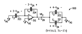
所定の利得に基づいて、第1のプログラム可能キャパシタを第1の静電容量に構成し、第2のプログラム可能キャパシタを第2の静電容量に構成し、
第1のフェーズにて、第1のプログラム可能キャパシタの第1の端子および第2のプログラム可能キャパシタの第1の端子を第1の入力端子に結合するように、かつ、第1のプログラム可能キャパシタの第2の端子および第2のプログラム可能キャパシタの第2の端子を電圧基準に結合するように、キャパシタネットワークを構成し、
第1のフェーズに続く第2のフェーズにて、第1のプログラム可能キャパシタの第1の端子を電圧基準に結合し、第1のプログラム可能キャパシタの第2の端子を増幅器の第1の入力に結合し、第2のプログラム可能キャパシタの第1の端子を増幅器の第1の出力に結合し、第2のプログラム可能キャパシタの第2の端子を増幅器の第1の入力に結合するように、キャパシタネットワークを構成するように構成されている、請求項2に記載のADCデバイス。 - 制御論理部は、
第2のモードにおいて、第1のプログラム可能キャパシタを第3の静電容量に構成し、第2のプログラム可能キャパシタを第3の静電容量に構成するように構成されている、請求項3に記載のADCデバイス。 - 第2のアナログ信号を受信する第2の入力端子を更に備え、
増幅器は、第1の入力、第2の入力、第1の出力、および第2の出力を備える、差動増幅器を含み、
アナログ部品は、前記増幅器の第2の入力と第2の出力とに結合しており複数のキャパシタを含む第2のキャパシタネットワークを更に備え、
制御論理部は、
第1のモードでは、第2のアナログ信号を前記所定の利得によって増幅して第2の増幅されたアナログ信号を生成する増幅構成に、増幅器および第2のキャパシタネットワークを構成し、
第2のモードでは、第2の増幅されたアナログ信号を用いて一つ又は複数の残留電圧からなる第2の一連の残留電圧を生成するように、増幅器および第2のキャパシタネットワークを構成するように構成されている、請求項1又は2に記載のADCデバイス。 - アナログ−デジタル変換器(ADC)の第1の入力端子において第1のアナログ信号を受信する工程と、
第1のアナログ信号を第1の利得によって増幅して第1の増幅されたアナログ信号を生成するように、ADCの増幅器および第1のキャパシタネットワークを構成する工程と、
第1の増幅されたアナログ信号に基づいて一つ又は複数の残留電圧からなる第1の一連の残留電圧を生成するように、増幅器および第1のキャパシタネットワークを構成する工程と、
ADCからの出力のために一つ又は複数の残留電圧からなる第1の一連の残留電圧に基づいてデジタル値を提供する工程と、を備え、
第1のアナログ信号を増幅するように、増幅器および第1のキャパシタネットワークを構成する工程は、
第1の利得に基づいて、第1の静電容量を有するように第1のキャパシタネットワークの第1のプログラム可能キャパシタを構成し、第2の静電容量を有するように第1のキャパシタネットワークの第2のプログラム可能キャパシタを構成する工程と、
第1のフェーズにて、
第1のプログラム可能キャパシタの第1の端子および第2のプログラム可能キャパシタの第1の端子を第1の入力端子に結合する工程と、
第1のプログラム可能キャパシタの第2の端子および第2のプログラム可能キャパシタの第2の端子を電圧基準に結合する工程と、 第1のフェーズに続く第2のフェーズにて、
第1のプログラム可能キャパシタの第2の端子および第2のプログラム可能キャパシタの第2の端子を増幅器の入力に結合する工程と、
第1のプログラム可能キャパシタの第1の端子を電圧基準に結合する工程と、
第2のプログラム可能キャパシタの第1の端子を増幅器の出力に結合する工程と、
第1のキャパシタネットワークにおける第3のキャパシタの第1の端子および第1のキャパシタネットワークにおける第4のキャパシタの第1の端子を増幅器の出力に結合する工程と、
第3のキャパシタの第2の端子および第4のキャパシタの第2の端子を電圧基準に結合する工程と、を含む方法。 - ADCの第1の入力端子において第2のアナログ信号を受信する工程と、
第2のアナログ信号を第1の利得と異なる第2の利得によって増幅して第2の増幅されたアナログ信号を生成するように、ADCの増幅器および第1のキャパシタネットワークを構成する工程と、
第2の増幅されたアナログ信号に基づいて一つ又は複数の残留電圧からなる第2の一連の残留電圧を生成するように、増幅器および第1のキャパシタネットワークを構成する工程と、
ADCからの出力のために一つ又は複数の残留電圧からなる第2の一連の残留電圧に基づいてデジタル値を提供する工程と、を含む請求項6に記載の方法。 - ADCの第2の入力端子において第2のアナログ信号を受信する工程と、
第2のアナログ信号を第1の利得によって増幅して第2の増幅されたアナログ信号を生成するように、ADCの増幅器および第2のキャパシタネットワークを構成する工程と、
第2の増幅されたアナログ信号に基づいて一つ又は複数の残留電圧からなる第2の一連の残留電圧を生成するように、増幅器および第2のキャパシタネットワークを構成する工程とを更に含み、
ADCからの出力のためにデジタル値を提供する工程は、出力のために一つ又は複数の残留電圧からなる第1の一連の残留電圧および一つ又は複数の残留電圧からなる第2の一連の残留電圧に基づいてデジタル値を提供することを含む、請求項7に記載の方法。
Applications Claiming Priority (3)
| Application Number | Priority Date | Filing Date | Title |
|---|---|---|---|
| US12/026,205 US7589658B2 (en) | 2008-02-05 | 2008-02-05 | Analog-to-digital converter with variable gain and method thereof |
| US12/026,205 | 2008-02-05 | ||
| PCT/US2009/030517 WO2009099700A2 (en) | 2008-02-05 | 2009-01-09 | Analog-to-digital converter with variable gain and method thereof |
Publications (3)
| Publication Number | Publication Date |
|---|---|
| JP2011511564A JP2011511564A (ja) | 2011-04-07 |
| JP2011511564A5 JP2011511564A5 (ja) | 2012-02-23 |
| JP5257955B2 true JP5257955B2 (ja) | 2013-08-07 |
Family
ID=40931145
Family Applications (1)
| Application Number | Title | Priority Date | Filing Date |
|---|---|---|---|
| JP2010545045A Expired - Fee Related JP5257955B2 (ja) | 2008-02-05 | 2009-01-09 | 可変利得をもつアナログ−デジタル変換器とその方法 |
Country Status (4)
| Country | Link |
|---|---|
| US (1) | US7589658B2 (ja) |
| JP (1) | JP5257955B2 (ja) |
| CN (1) | CN101939918B (ja) |
| WO (1) | WO2009099700A2 (ja) |
Families Citing this family (16)
| Publication number | Priority date | Publication date | Assignee | Title |
|---|---|---|---|---|
| US8862253B2 (en) * | 2007-04-30 | 2014-10-14 | Sigmatel, Inc. | Gain control module and applications thereof |
| US20100060494A1 (en) * | 2008-09-09 | 2010-03-11 | Atmel Corporation | Analog to Digital Converter |
| US7911370B2 (en) * | 2009-06-25 | 2011-03-22 | Mediatek Inc. | Pipeline analog-to-digital converter with programmable gain function |
| US8339302B2 (en) * | 2010-07-29 | 2012-12-25 | Freescale Semiconductor, Inc. | Analog-to-digital converter having a comparator for a multi-stage sampling circuit and method therefor |
| US8384579B2 (en) * | 2011-07-19 | 2013-02-26 | Freescale Semiconductor, Inc. | Systems and methods for data conversion |
| US8531324B2 (en) | 2011-07-19 | 2013-09-10 | Freescale Semiconductor, Inc. | Systems and methods for data conversion |
| US8525721B2 (en) * | 2011-09-20 | 2013-09-03 | Freescale Semiconductor, Inc. | Low power cycle data converter |
| JP5436508B2 (ja) * | 2011-09-22 | 2014-03-05 | 独立行政法人科学技術振興機構 | アナログ‐デジタル変換器及びアナログ信号をデジタル信号に変換する方法 |
| US8823566B2 (en) | 2012-06-29 | 2014-09-02 | Freescale Semiconductor, Inc | Analog to digital conversion architecture and method with input and reference voltage scaling |
| US8860596B1 (en) * | 2013-08-20 | 2014-10-14 | Freescale Semiconductor, Inc. | Redundant signed digit (RSD) analog to digital converter |
| JP6849903B2 (ja) * | 2016-10-06 | 2021-03-31 | 株式会社ソシオネクスト | 受信回路及び半導体集積回路 |
| KR102431230B1 (ko) * | 2017-11-17 | 2022-08-10 | 에스케이하이닉스 주식회사 | 저잡음 싱글-슬롭 비교 장치 및 그에 따른 아날로그-디지털 변환 장치와 씨모스 이미지 센서 |
| US10069507B1 (en) | 2018-04-06 | 2018-09-04 | Nxp Usa, Inc. | Mismatch and reference common-mode offset insensitive single-ended switched capacitor gain stage |
| US10651811B2 (en) | 2018-05-18 | 2020-05-12 | Nxp Usa, Inc. | Mismatch and reference common-mode offset insensitive single-ended switched capacitor gain stage with reduced capacitor mismatch sensitivity |
| US10979064B2 (en) | 2018-10-31 | 2021-04-13 | Taiwan Semiconductor Manufacturing Company, Ltd. | Analog to digital converter with inverter based amplifier |
| JP2022130998A (ja) * | 2021-02-26 | 2022-09-07 | セイコーエプソン株式会社 | A/dコンバーター、デジタル出力温度センサー、回路装置及び発振器 |
Family Cites Families (27)
| Publication number | Priority date | Publication date | Assignee | Title |
|---|---|---|---|---|
| US4710724A (en) | 1986-04-02 | 1987-12-01 | Motorola, Inc. | Differential CMOS comparator for switched capacitor applications |
| US5625361A (en) | 1994-11-14 | 1997-04-29 | Motorola, Inc. | Programmable capacitor array and method of programming |
| US5644313A (en) * | 1995-06-05 | 1997-07-01 | Motorola, Inc. | Redundant signed digit A-to-D conversion circuit and method thereof |
| US5574457A (en) | 1995-06-12 | 1996-11-12 | Motorola, Inc. | Switched capacitor gain stage |
| US5680070A (en) | 1996-02-05 | 1997-10-21 | Motorola, Inc. | Programmable analog array and method for configuring the same |
| US5710563A (en) | 1997-01-09 | 1998-01-20 | National Semiconductor Corporation | Pipeline analog to digital converter architecture with reduced mismatch error |
| JPH11122197A (ja) * | 1997-10-17 | 1999-04-30 | Sony Corp | アラーム通知装置 |
| US6195032B1 (en) | 1999-08-12 | 2001-02-27 | Centillium Communications, Inc. | Two-stage pipelined recycling analog-to-digital converter (ADC) |
| US6420991B1 (en) | 1999-09-08 | 2002-07-16 | Texas Instruments Incorporated | Dynamic element matching for converting element mismatch into white noise for a pipelined analog to digital converter |
| US6362770B1 (en) | 2000-09-12 | 2002-03-26 | Motorola, Inc. | Dual input switched capacitor gain stage |
| US6617992B2 (en) | 2001-08-15 | 2003-09-09 | National Semiconductor Corporation | Capacitor mismatch independent gain stage for differential pipeline analog to digital converters |
| US6535157B1 (en) * | 2001-09-07 | 2003-03-18 | Motorola, Inc. | Low power cyclic A/D converter |
| US6489914B1 (en) * | 2001-12-04 | 2002-12-03 | Motorola, Inc. | RSD analog to digital converter |
| US6741194B1 (en) | 2002-12-23 | 2004-05-25 | Motorola, Inc. | Methods and apparatus for detecting out-of-range signals in an analog-to-digital converter |
| US6927722B2 (en) | 2003-05-20 | 2005-08-09 | Freescale Semiconductor, Inc. | Series capacitive component for switched-capacitor circuits consisting of series-connected capacitors |
| US6909393B2 (en) | 2003-07-30 | 2005-06-21 | Freescale Semiconductor, Inc. | Space efficient low power cyclic A/D converter |
| JP3962788B2 (ja) * | 2003-10-29 | 2007-08-22 | 国立大学法人静岡大学 | A/d変換アレイ及びイメージセンサ |
| US7068202B2 (en) | 2003-12-31 | 2006-06-27 | Conexant Systems, Inc. | Architecture for an algorithmic analog-to-digital converter |
| US6967611B2 (en) | 2004-03-19 | 2005-11-22 | Freescale Semiconductor, Inc. | Optimized reference voltage generation using switched capacitor scaling for data converters |
| US7015852B1 (en) | 2004-11-30 | 2006-03-21 | Freescale Semiconductor, Inc. | Cyclic analog-to-digital converter |
| US7009549B1 (en) | 2004-12-30 | 2006-03-07 | Texas Instruments Incorporated | Switched-capacitor circuit with scaled reference voltage |
| US7102365B1 (en) | 2005-04-01 | 2006-09-05 | Freescale Semiconductor, Inc. | Apparatus for current sensing |
| US7307572B2 (en) | 2005-06-15 | 2007-12-11 | Freescale Semiconductor, Inc. | Programmable dual input switched-capacitor gain stage |
| US7064700B1 (en) | 2005-06-15 | 2006-06-20 | Freescale Semiconductor, Inc. | Multi-channel analog to digital converter |
| US7289052B1 (en) | 2006-04-25 | 2007-10-30 | Freescale Semiconductor, Inc. | System and method for analog-to-digital conversion |
| JP2008028820A (ja) * | 2006-07-24 | 2008-02-07 | Sharp Corp | A/dコンバータ |
| JP4811339B2 (ja) * | 2006-09-21 | 2011-11-09 | 株式会社デンソー | A/d変換器 |
-
2008
- 2008-02-05 US US12/026,205 patent/US7589658B2/en not_active Expired - Fee Related
-
2009
- 2009-01-09 JP JP2010545045A patent/JP5257955B2/ja not_active Expired - Fee Related
- 2009-01-09 CN CN2009801042437A patent/CN101939918B/zh not_active Expired - Fee Related
- 2009-01-09 WO PCT/US2009/030517 patent/WO2009099700A2/en active Application Filing
Also Published As
| Publication number | Publication date |
|---|---|
| US20090195428A1 (en) | 2009-08-06 |
| WO2009099700A2 (en) | 2009-08-13 |
| CN101939918A (zh) | 2011-01-05 |
| JP2011511564A (ja) | 2011-04-07 |
| US7589658B2 (en) | 2009-09-15 |
| CN101939918B (zh) | 2013-10-23 |
| WO2009099700A3 (en) | 2009-10-01 |
Similar Documents
| Publication | Publication Date | Title |
|---|---|---|
| JP5257955B2 (ja) | 可変利得をもつアナログ−デジタル変換器とその方法 | |
| US6967611B2 (en) | Optimized reference voltage generation using switched capacitor scaling for data converters | |
| US7307572B2 (en) | Programmable dual input switched-capacitor gain stage | |
| US8031098B1 (en) | DAC circuit with pseudo-return-to-zero scheme and DAC calibration circuit and method | |
| TWI521887B (zh) | 連續近似式類比數位轉換器 | |
| US8860600B1 (en) | Successive-approximation-register analog-to-digital converter for programmably amplifying amplitude of input signal and method thereof | |
| US8754794B1 (en) | Methods and apparatus for calibrating pipeline analog-to-digital converters | |
| US7224306B2 (en) | Analog-to-digital converter in which settling time of amplifier circuit is reduced | |
| US8514123B2 (en) | Compact SAR ADC | |
| US7956780B2 (en) | Filter with capacitive forward coupling | |
| US7629906B2 (en) | Circuit and method for calibrating direct current offset | |
| CN105959008A (zh) | 预放大器以及包括其的比较器和模数转换装置 | |
| WO2013036204A1 (en) | An analog-to-digital converter for a multi-channel signal acquisition system | |
| KR101435978B1 (ko) | 이중채널 sar 및 플래쉬 adc를 이용한 하이브리드 파이프라인 adc | |
| US9300312B2 (en) | Analog-digital converter | |
| US20180167075A1 (en) | Hybrid analog-to-digital converter | |
| US7002507B2 (en) | Pipelined and cyclic analog-to-digital converters | |
| US11233521B2 (en) | Sub-ranging analog to digital converter | |
| US8264393B2 (en) | Current reduction in a single stage cyclic analog to digital converter with variable resolution | |
| WO2012079077A1 (en) | Circuits and methods for implementing a residue amplifier | |
| US20130002468A1 (en) | Analog-digital converter | |
| US6859158B2 (en) | Analog-digital conversion circuit | |
| JP2010278952A (ja) | 逐次比較型ad変換回路及び半導体集積回路 | |
| TWI446726B (zh) | 連續逼近暫存式類比數位轉換器 | |
| JP2011188250A (ja) | 時定数調整回路 |
Legal Events
| Date | Code | Title | Description |
|---|---|---|---|
| A521 | Written amendment |
Free format text: JAPANESE INTERMEDIATE CODE: A523 Effective date: 20120106 |
|
| A621 | Written request for application examination |
Free format text: JAPANESE INTERMEDIATE CODE: A621 Effective date: 20120106 |
|
| RD04 | Notification of resignation of power of attorney |
Free format text: JAPANESE INTERMEDIATE CODE: A7424 Effective date: 20120227 |
|
| A977 | Report on retrieval |
Free format text: JAPANESE INTERMEDIATE CODE: A971007 Effective date: 20120629 |
|
| A131 | Notification of reasons for refusal |
Free format text: JAPANESE INTERMEDIATE CODE: A131 Effective date: 20120724 |
|
| A521 | Written amendment |
Free format text: JAPANESE INTERMEDIATE CODE: A523 Effective date: 20121023 |
|
| A02 | Decision of refusal |
Free format text: JAPANESE INTERMEDIATE CODE: A02 Effective date: 20121113 |
|
| A521 | Written amendment |
Free format text: JAPANESE INTERMEDIATE CODE: A523 Effective date: 20130227 |
|
| A911 | Transfer to examiner for re-examination before appeal (zenchi) |
Free format text: JAPANESE INTERMEDIATE CODE: A911 Effective date: 20130307 |
|
| TRDD | Decision of grant or rejection written | ||
| A01 | Written decision to grant a patent or to grant a registration (utility model) |
Free format text: JAPANESE INTERMEDIATE CODE: A01 Effective date: 20130326 |
|
| A61 | First payment of annual fees (during grant procedure) |
Free format text: JAPANESE INTERMEDIATE CODE: A61 Effective date: 20130417 |
|
| FPAY | Renewal fee payment (event date is renewal date of database) |
Free format text: PAYMENT UNTIL: 20160502 Year of fee payment: 3 |
|
| R150 | Certificate of patent or registration of utility model |
Free format text: JAPANESE INTERMEDIATE CODE: R150 |
|
| R250 | Receipt of annual fees |
Free format text: JAPANESE INTERMEDIATE CODE: R250 |
|
| LAPS | Cancellation because of no payment of annual fees |