JP5257955B2 - Analog-to-digital converter with variable gain and method thereof - Google Patents
Analog-to-digital converter with variable gain and method thereof Download PDFInfo
- Publication number
- JP5257955B2 JP5257955B2 JP2010545045A JP2010545045A JP5257955B2 JP 5257955 B2 JP5257955 B2 JP 5257955B2 JP 2010545045 A JP2010545045 A JP 2010545045A JP 2010545045 A JP2010545045 A JP 2010545045A JP 5257955 B2 JP5257955 B2 JP 5257955B2
- Authority
- JP
- Japan
- Prior art keywords
- terminal
- capacitor
- amplifier
- input
- analog signal
- Prior art date
- Legal status (The legal status is an assumption and is not a legal conclusion. Google has not performed a legal analysis and makes no representation as to the accuracy of the status listed.)
- Expired - Fee Related
Links
Images


Classifications
-
- H—ELECTRICITY
- H03—ELECTRONIC CIRCUITRY
- H03M—CODING; DECODING; CODE CONVERSION IN GENERAL
- H03M1/00—Analogue/digital conversion; Digital/analogue conversion
- H03M1/12—Analogue/digital converters
- H03M1/18—Automatic control for modifying the range of signals the converter can handle, e.g. gain ranging
- H03M1/186—Automatic control for modifying the range of signals the converter can handle, e.g. gain ranging in feedforward mode, i.e. by determining the range to be selected directly from the input signal
-
- H—ELECTRICITY
- H03—ELECTRONIC CIRCUITRY
- H03M—CODING; DECODING; CODE CONVERSION IN GENERAL
- H03M1/00—Analogue/digital conversion; Digital/analogue conversion
- H03M1/06—Continuously compensating for, or preventing, undesired influence of physical parameters
- H03M1/0617—Continuously compensating for, or preventing, undesired influence of physical parameters characterised by the use of methods or means not specific to a particular type of detrimental influence
- H03M1/0675—Continuously compensating for, or preventing, undesired influence of physical parameters characterised by the use of methods or means not specific to a particular type of detrimental influence using redundancy
- H03M1/0678—Continuously compensating for, or preventing, undesired influence of physical parameters characterised by the use of methods or means not specific to a particular type of detrimental influence using redundancy using additional components or elements, e.g. dummy components
- H03M1/068—Continuously compensating for, or preventing, undesired influence of physical parameters characterised by the use of methods or means not specific to a particular type of detrimental influence using redundancy using additional components or elements, e.g. dummy components the original and additional components or elements being complementary to each other, e.g. CMOS
- H03M1/0682—Continuously compensating for, or preventing, undesired influence of physical parameters characterised by the use of methods or means not specific to a particular type of detrimental influence using redundancy using additional components or elements, e.g. dummy components the original and additional components or elements being complementary to each other, e.g. CMOS using a differential network structure, i.e. symmetrical with respect to ground
-
- H—ELECTRICITY
- H03—ELECTRONIC CIRCUITRY
- H03M—CODING; DECODING; CODE CONVERSION IN GENERAL
- H03M1/00—Analogue/digital conversion; Digital/analogue conversion
- H03M1/12—Analogue/digital converters
- H03M1/34—Analogue value compared with reference values
- H03M1/38—Analogue value compared with reference values sequentially only, e.g. successive approximation type
- H03M1/40—Analogue value compared with reference values sequentially only, e.g. successive approximation type recirculation type
- H03M1/403—Analogue value compared with reference values sequentially only, e.g. successive approximation type recirculation type using switched capacitors
-
- H—ELECTRICITY
- H03—ELECTRONIC CIRCUITRY
- H03M—CODING; DECODING; CODE CONVERSION IN GENERAL
- H03M1/00—Analogue/digital conversion; Digital/analogue conversion
- H03M1/12—Analogue/digital converters
- H03M1/34—Analogue value compared with reference values
- H03M1/38—Analogue value compared with reference values sequentially only, e.g. successive approximation type
- H03M1/44—Sequential comparisons in series-connected stages with change in value of analogue signal
- H03M1/442—Sequential comparisons in series-connected stages with change in value of analogue signal using switched capacitors
Landscapes
- Engineering & Computer Science (AREA)
- Theoretical Computer Science (AREA)
- Analogue/Digital Conversion (AREA)
- Amplifiers (AREA)
- Control Of Amplification And Gain Control (AREA)
Description
本開示は、全体的にアナログ−デジタル変換に関しており、特に、冗長符号付きディジット(RSD)ベースのアナログ−デジタル変換に関する。 The present disclosure relates generally to analog-to-digital conversion, and more particularly to redundant signed digit (RSD) based analog-to-digital conversion.
アナログ、デジタルの混合したデバイスは、デバイスのデジタル部品による使用のために、アナログ−デジタル変換器(ADC)を用いて、アナログ信号の電圧を対応するデジタル値に変換する。冗長符号付きディジット(RSD)ベースのADCは、一定の種類のシステム、特に電力および空間が貴重なシステムでは、特に有益な場合がしばしばある。RSD ADCは一般的に、一連の段を介して、アナログ信号を対応するデジタル値に変換する。初期状態において、入力されたアナログ信号の電圧は、二つ以上の基準電圧、例えば、VH,VLと比較される。これらの比較の結果から、初期段のコードビットが生じる。増幅器と一組のキャパシタとを備えるアナログ回路を用いて残留電圧を決定する。第2の段では、この残留電圧を用いて基準電圧との比較処理を繰り返し、第2の段のコードビットを生成する。この処理、すなわち、前の段の残留電圧から残留電圧を計算し、得られる残留電圧を比較してコード値を生成する処理は、適正な解に達するまで、数多くの段に渡って繰り返され得る。次に、アナログ信号を表すデジタル値を生成するために、各段からのコード値に対しRSDアルゴリズムが適用される。 A mixed analog, digital device uses an analog-to-digital converter (ADC) to convert the voltage of the analog signal into a corresponding digital value for use by the digital components of the device. Redundant signed digit (RSD) based ADCs are often particularly beneficial in certain types of systems, especially those where power and space are at a premium. RSD ADCs typically convert an analog signal into a corresponding digital value through a series of stages. In the initial state, the voltage of the input analog signal is compared with two or more reference voltages, for example, VH and VL. As a result of these comparisons, an initial stage code bit is generated. The residual voltage is determined using an analog circuit comprising an amplifier and a set of capacitors. In the second stage, the comparison process with the reference voltage is repeated using the residual voltage, and the code bit of the second stage is generated. This process, i.e., calculating the residual voltage from the residual voltage of the previous stage and comparing the resulting residual voltage to generate a code value, can be repeated over many stages until the proper solution is reached. . The RSD algorithm is then applied to the code value from each stage to generate a digital value representing the analog signal.
動作環境によっては、異なるアナログ信号源が、同じRSD ADCを使用しながらも、異なる電圧レベルで動作する場合がある。例示すると、自動車の環境では、異なるセンサが、同じ制御プロセッサによる処理用のデジタル値への変換のために、異なる電圧レベルのセンサ出力信号を提供する場合がある。適正な変換を保証するために、入力アナログ信号の各々は一般的に、変換前に所定の電圧レベルに増減される必要がある。従来のデバイスでは、この増減は、RSD ADCの入力より前に、利得回路を介して行われる。この別個の利得回路は、RSD ADCが設けられる集積回路の寸法および電力消費を増やすだけでなく、RSD ADCの設計および組立を複雑なものとする。 Depending on the operating environment, different analog signal sources may operate at different voltage levels while using the same RSD ADC. Illustratively, in an automotive environment, different sensors may provide sensor output signals at different voltage levels for conversion to digital values for processing by the same control processor. In order to ensure proper conversion, each of the input analog signals generally needs to be scaled to a predetermined voltage level before conversion. In conventional devices, this increase / decrease is done via a gain circuit prior to the input of the RSD ADC. This separate gain circuit not only increases the size and power consumption of the integrated circuit in which the RSD ADC is provided, but also complicates the design and assembly of the RSD ADC.
したがって、デジタル変換用にアナログ信号を増減させる改善された技術が好ましい。 Therefore, an improved technique for increasing or decreasing analog signals for digital conversion is preferred.
本開示は、添付の図面を参照することによって、よりよく理解され、その数多くの特徴と利点が当業者に明らかとなる。異なる図面で同じ参照記号を用いる場合、同様の又は同一の項目を意味している。 The present disclosure is better understood and its numerous features and advantages will become apparent to those skilled in the art by reference to the accompanying drawings. The use of the same reference symbols in different drawings indicates similar or identical items.
本開示の一つの態様では、冗長符号付きディジット(RSD)アナログ−デジタル変換器(ADC)デバイスは、アナログ信号を受信するための入力端子と、アナログ部品と、制御論理部とを含んでいる。アナログ部品は、入力と出力とを有する増幅器と、増幅器の入力と出力とに結合したキャパシタネットワークとを含んでいる。キャパシタネットワークは複数のキャパシタを備えている。制御論理部は、第1のモードでは、キャパシタネットワークおよび増幅器を、アナログ信号を所定の利得によって増幅し、増幅されたアナログ信号を生成する増幅構成に構成するように構成されている。さらに制御論理部は、第2のモードでは、キャパシタネットワークおよび増幅器を、増幅されたアナログ信号を用いて一つ又は複数の残留電圧からなる一連の残留電圧を生成するRSD構成に構成するように構成されている。 In one aspect of the present disclosure, a redundant signed digit (RSD) analog-to-digital converter (ADC) device includes an input terminal for receiving an analog signal, analog components, and control logic. The analog component includes an amplifier having an input and an output, and a capacitor network coupled to the input and output of the amplifier. The capacitor network includes a plurality of capacitors. In the first mode, the control logic unit is configured to configure the capacitor network and the amplifier in an amplification configuration that amplifies an analog signal with a predetermined gain and generates an amplified analog signal. Further, the control logic unit is configured to configure the capacitor network and the amplifier in an RSD configuration that generates a series of residual voltages of one or more residual voltages using the amplified analog signal in the second mode. Has been.
本開示の別の態様では、方法は、RSD ADCの入力端子でアナログ信号を受信する工程と、アナログ信号を所定の利得によって増幅し、増幅されたアナログ信号を生成するように、RSD ADCのキャパシタネットワークと増幅器とを構成する工程とを含んでいる。この方法は、増幅されたアナログ信号に基づいて一連の一つ又は複数の残留電圧を生成するように、キャパシタネットワークと増幅器とを構成する工程を更に含んでいる。この方法は、RSD ADCからの出力のために一連の一つ又は複数の残留電圧に基づいてデジタル値を提供する工程を更に含んでいる。 In another aspect of the present disclosure, a method includes receiving an analog signal at an input terminal of an RSD ADC and a capacitor of the RSD ADC so as to amplify the analog signal by a predetermined gain and generate an amplified analog signal. Forming a network and an amplifier. The method further includes configuring the capacitor network and the amplifier to generate a series of one or more residual voltages based on the amplified analog signal. The method further includes providing a digital value based on a series of one or more residual voltages for output from the RSD ADC.
図1〜17は、入力アナログ信号用の集積された可変利得段を採用する、冗長符号付きディジット(RSD)アナログ−デジタル変換器(ADC)を用いて、アナログ信号を対応するデジタル値に変換する技術の例を示す。RSD ADCのアナログ部品の増幅器およびキャパシタネットワークは共に、入力アナログ信号を増幅して、RSD変換のための残留電圧を計算するように用いられる。一実施形態では、キャパシタは、入力アナログ信号を所定の電圧レベルに再帰的に増幅するように、キャパシタ構成のシーケンスに編成される。増幅されると、キャパシタは、増幅されたアナログ信号から始まる一連の一つ又は複数のRSD残留電圧を生成するように再構成される。別の実施形態では、調整可能な静電容量を有するプログラム可能なキャパシタが、入力アナログ信号を所定の電圧レベルに増幅するために所定の利得を提供するように、ある静電容量に構成される。次いで、プログラム可能なキャパシタは、増幅されたアナログ信号から始まるRSD残留電圧の計算を行うために、他の静電容量に再構成される。増幅されたアナログ信号を用いる入力アナログ信号の可変利得とRSD残留電圧との両方のために、RSD ADCのキャパシタおよび増幅器を二重に使用することによって、別個のフロントエンド利得回路を有する従来のRSD ADCの実装と比べ、RSD ADCの寸法、複雑さ、および電力消費を減少できる。 1-17 convert an analog signal to a corresponding digital value using a redundant signed digit (RSD) analog-to-digital converter (ADC) that employs an integrated variable gain stage for the input analog signal. An example of the technology is shown. Both the RSD ADC analog component amplifier and capacitor network are used to amplify the input analog signal and calculate the residual voltage for RSD conversion. In one embodiment, the capacitors are organized into a sequence of capacitor configurations to recursively amplify the input analog signal to a predetermined voltage level. Once amplified, the capacitor is reconfigured to produce a series of one or more RSD residual voltages starting from the amplified analog signal. In another embodiment, a programmable capacitor having an adjustable capacitance is configured with a capacitance so as to provide a predetermined gain for amplifying the input analog signal to a predetermined voltage level. . The programmable capacitor is then reconfigured to another capacitance to perform RSD residual voltage calculations starting from the amplified analog signal. Conventional RSD with separate front-end gain circuit by double use of RSD ADC capacitor and amplifier for both variable gain and RSD residual voltage of input analog signal with amplified analog signal Compared to an ADC implementation, the size, complexity, and power consumption of the RSD ADC can be reduced.
ここで用いる“キャパシタ”という用語は、特定の静電容量を提供するように構成されている又は構成できる一つ又は複数の容量性部品を意味する。例示すると、キャパシタは、特定の静電容量を提供するために、特定の静電容量を提供する単一の容量性部品として、又は並列、直列、もしくはその組み合わせで接続した容量性部品のネットワークとして設置できる。キャパシタは、集積されたキャパシタ(例えば、集積回路の一つ又は複数の層に設けられた一つ又は複数の容量性構造)又は個別のキャパシタとして設置できる。更に、本明細書において更に詳細に説明するように、キャパシタは、調整可能な静電容量を有するプログラム可能なキャパシタを含んでよい。その一例は米国特許第5,625,361号明細書に記載されている。その全体を引用により本明細書に援用する。 As used herein, the term “capacitor” means one or more capacitive components that are or can be configured to provide a particular capacitance. To illustrate, a capacitor is a single capacitive component that provides a specific capacitance, or as a network of capacitive components connected in parallel, series, or a combination thereof to provide a specific capacitance. Can be installed. The capacitors can be installed as integrated capacitors (eg, one or more capacitive structures provided in one or more layers of an integrated circuit) or as individual capacitors. Further, as described in more detail herein, the capacitor may include a programmable capacitor having an adjustable capacitance. One example is described in US Pat. No. 5,625,361. Which is incorporated herein by reference in its entirety.
容易な図解とするために、本明細書に開示の技術は、単一のRSD段がサンプリングおよび増幅のサイクルからなるシーケンスを再帰的に巡るように用いられる、RSDの実装の一例に関連して説明される。ここで、一つのサンプリング段のRSD段から出力された残留電圧は、次のサンプリング段において次の残留電圧を計算する際に用いられる。サイクル式の単一段RSD実装の一例は、米国特許第6,535,157号明細書に記載されている。その全体を引用により本明細書に援用する。他の実施形態では、開示の技術は、二つ以上のRSD段のシーケンスを有するRSD実装での使用に適用でき、その場合、一つのRSD段で出力された残留電圧が次のRSD段に入力される。多段RSD実装の一例は、米国特許第5,664,313号明細書に記載されている。その全体を引用によって本明細書に援用する。 For ease of illustration, the techniques disclosed herein relate to an example of an RSD implementation in which a single RSD stage is used to recursively cycle through a sequence of sampling and amplification cycles. Explained. Here, the residual voltage output from the RSD stage of one sampling stage is used when calculating the next residual voltage in the next sampling stage. An example of a cycled single stage RSD implementation is described in US Pat. No. 6,535,157. Which is incorporated herein by reference in its entirety. In other embodiments, the disclosed technique can be applied for use in an RSD implementation having a sequence of two or more RSD stages, in which case the residual voltage output from one RSD stage is input to the next RSD stage. Is done. An example of a multistage RSD implementation is described in US Pat. No. 5,664,313. Which is incorporated herein by reference in its entirety.
図1は、本開示の少なくとも一つの実施形態による、アナログ−デジタル(A/D)変換システム100の一例を示す。A/D変換システム100は、電圧セレクタ104から電圧VINを有するアナログ信号を受信するための入力端子と、電圧VINを表すデジタル値(“DATA”)を提供する出力とを備える、RSD ADC102を含んでいる。RSD ADC102は、アナログ部品106と、制御論理部108と、デジタル変換論理部110とを含んでいる。アナログ部品106は、増幅器112を備えた利得回路と、本明細書に記載の数多くの構成に編成できる複数のキャパシタを備えたキャパシタネットワーク114とを含んでいる。利得回路およびキャパシタネットワーク114は共に、入力アナログ信号を増幅し、増幅された信号を用いて一連の残留電圧を次に生成するためのものである。
FIG. 1 illustrates an example of an analog-to-digital (A / D)
少なくとも一つの実施形態では、A/D変換システム100は、変換されるアナログ信号が異なる電圧レベルを有する環境において実装される。例示すると、A/D変換システム100は、様々な自動車のセンサからの出力信号を、それらの対応するデジタル値に変換するように、自動車環境に設置できる。したがって、電圧セレクタ104は、異なる電圧レベルを有し得る複数のアナログ信号(S1〜Sn)を入力として受信し、RSD ADC102への入力のためにそれらのアナログ信号のうちの一つを選択する。アナログ信号が異なる電圧レベルを有する場合にアナログ信号をそれらの対応する値に適正に変換するために、RSD ADC102は、入力信号を共通の電圧レベルに増幅し、次に、増幅された信号を対応するデジタル値に変換する。例示すると、三つの異なる電圧レベル、例えば、1ボルト、2ボルト、4ボルトが存在する場合、1ボルトのレベルのアナログ信号は利得4だけ増幅でき、2ボルトのレベルのアナログ信号は利得2だけ増幅できるので、全てのアナログ信号が4ボルトのレベルで処理できる。
In at least one embodiment, the A /
この入力信号の初期増幅のために、制御論理部108は、増幅器112およびキャパシタネットワーク114を一つ又は複数のキャパシタ構成のシーケンスに構成して、入力信号の所望の増幅を達成する。制御論理部108は、次に、増幅された入力信号から始まる冗長符号付きディジット計算用のRSD構成のシーケンスに、増幅器112およびキャパシタネットワーク114を構成する。多キャパシタ構成を用いる、アナログ部品106のシングルエンド型実装の一例が、図3〜8を参照して以下に説明される。アナログ部品106の差動信号方式の実装が、図9〜12を参照して以下に説明される。同時の増幅を伴う、または伴わない、シングルエンド型の差動変換のために構成されたアナログ部品106の実装の一例が、図9および13〜15を参照して以下に説明される。アナログ部品106のプログラム可能なキャパシタベースの実装が、図16および17を参照して以下に説明される。
For this initial amplification of the input signal,
各RSD計算段で、デジタル変換論理部110は、得られる電圧(最初は、増幅されたアナログ信号の電圧、その後は、残留電圧)を比較して、各RSD計算段におけるコード値を生成する。デジタル変換論理部110は、次いで、RSD計算段からのコードビット値を整合させ、同期化し、加算して、RSDアルゴリズムに従って出力デジタル値DATAを生成する。コードビットからデジタル値を生成する処理の一例が、上述の米国特許第5,644,313号明細書に記載されている。
In each RSD calculation stage, the digital
図2は、本開示の少なくとも一つの実施形態による、図1のRSD ADC102による電圧VINを有するアナログ信号の変換の一例の方法200を示す。この方法200は、増幅モード(ブロック202)と、それに続くRSD変換モード(ブロック204)とを含んでいる。ブロック202の処理は、ブロック206,208,210で表されている。
FIG. 2 illustrates an
ブロック202にて、入力アナログ信号がRSD ADC102で受信され、制御論理部108は、入力アナログ信号がより高い電圧レベルに増幅されるように構成されるか否かを決定する(例えば、4ボルトのレベルから16ボルトのレベルに)。増幅が必要な場合、制御論理部108は、ブロック206にて入力アナログ信号の電圧VINをサンプリングする初期サンプリング構成に、キャパシタネットワーク114を構成する。ブロック208にて、制御論理部108は、ブロック206のサンプリング処理から生じるキャパシタネットワーク114のキャパシタに加わる電圧を用いて電圧VINを増幅する増幅構成に、キャパシタネットワーク114を構成する。一実施形態では、増幅構成の利得は、キャパシタの相対静電容量など、様々な特性によって制限されるので、電圧VINは、ブロック206,208の処理における初期の印加の後、十分に増幅されない場合がある。そこで、ブロック206の処理は、電圧VINの所望の増幅に達するまで、得られる増幅された電圧に対して1回以上繰り返すことができる。例示すると、入力アナログ信号が4ボルトの電圧レベルを有すると仮定すると、RSD ADC102は16ボルトのレベルで電圧を変換するように構成され、アナログ部品106は反復毎に2X利得を提供するように構成できる。この場合、電圧VINを4ボルトのレベルから16ボルトのレベルまで増幅するには、4Xの利得が必要になるので、増幅処理は、4X利得を得るために2回繰り返される。ブロック206,208の処理の1回目の通過(パス)の後には、電圧VINはVamp1=2×VINに増幅される。ブロック206,208の処理の2回目のパスの後には、増幅されたVamp1がVamp2=2×Vamp1=4×VINに増幅される。ブロック210にて十分な利得が得られていると、方法200はブロック204に進む。
At
ブロック204にて、制御論理部108はキャパシタネットワーク114を一連のRSD構成に構成し、増幅された電圧は、上述の米国特許第5,644,313号明細書および米国特許第6,535,157号明細書に記載されたものなど、RSD変換処理を用いて、アナログ部品106およびデジタル変換論理部110を介してデジタル値に変換される。得られるデジタル値は、次に、必要に応じて、システムのデジタル部品によって処理される。
At
図3は、本開示の少なくとも一つの実施形態による、RSD ADCのシングルエンド型の実装の一例を示す。図示されたRSD ADC302(図1のRSD ADC102に相当)は、アナログ部品306と、制御論理部308と、デジタル変換論理部310とを含んでいる。アナログ部品306は、増幅器312と、スイッチング回路320を備えたキャパシタネットワーク314と、四つのキャパシタ321,322,323,324(まとめて、キャパシタ321〜324)のような複数のキャパシタとを含んでいる。スイッチング回路320は、複数のスイッチ(例えば、トランジスタ又はパスゲート)と、増幅器312の入力端子(例えば、マイナス(−)入力端子)に接続した端子と、増幅器312の出力端子に接続した端子とを含んでいる。スイッチング回路320は、入力アナログ信号(VIN)、一つ又は複数の基準電圧(例えば、VREF+とVREF−)、および複数のスイッチ制御信号SW1〜SWnを受信するための入力を含んでいる。スイッチ制御信号は、本明細書においてより詳細に説明されるように、キャパシタ321〜324の様々な構成に影響を与えるようにスイッチに対し送られる。スイッチング回路320は、出力電圧を提供する出力を更に備えており、この出力電圧は、RSD ADC302の動作の特定の段に応じて、電圧VIN、電圧VINの増幅されたもの、又は残留電圧(VR)のいずれかを含む。
FIG. 3 illustrates an example of a single-ended implementation of an RSD ADC according to at least one embodiment of the present disclosure. The illustrated RSD ADC 302 (corresponding to the
制御論理部308は、一つ又は複数のクロック信号(CLK)を受信するための入力と、イネーブル(EN)信号およびスイッチ制御信号SW1〜SWnを提供する出力とを含んでいる。少なくとも一つの実施形態において、制御論理部308は、スイッチング回路320を介してキャパシタ321〜324の様々な構成に影響を与えると共に一つ又は複数のクロック信号のフェーズに基づいてデジタル変換論理部310を作動可能または作動不能にするように、スイッチ制御信号SW1〜SWnおよびEN信号を構成する。
The
デジタル変換論理部310は、比較器332,334とRSD加算器336とを含んでいる。比較器332は、スイッチング回路320から出力電圧を受信するための入力と、第1の基準電圧(VH)を受信するための入力と、出力電圧と第1の基準電圧との比較に基づく値を提供する出力とを含んでいる。比較器334は、スイッチング回路320の出力電圧を受信するための入力と、第2の基準電圧(VL)を受信するための入力と、出力電圧と第2の基準電圧との比較に基づく値を提供する出力とを含んでいる。RSD加算器336は、比較器332,334から値を受信するための入力と、入力アナログ信号をデジタル値に変換するために行われる対応するRSD段中に比較器332,334によって出力される値のシーケンスに対し適用される整合、同期化、および加算の処理に基づいて出力デジタル値(“DATA”)の対応するビットを提供する複数の出力とを含んでいる。更に、一実施形態では、制御論理部308は、比較器332,334から値を受信すると共に、RSD変換処理中にVREF+又はVREF−の導入を制御するように、その比較器332,334からの値に基づいて三つの信号(h,l,m)を生成する。比較器332,334およびRSD加算器336は、制御論理部308からEN信号を受信するための入力を更に含むことができ、その場合、それらの部品は、EN信号が作動不能状態にあるとき(例えば、アサート停止)に作動不能になる(例えば、クロックゲート制御されるか、電源から切断される)。
The digital
少なくとも一つの実施形態では、制御論理部308は、図3の状態図340が表す動作を有するハードウェア状態機械を実装する。アイドル状態342にて、制御論理部308はEN信号を作動不能状態に構成することによって、RSD ADC302の部品をアイドル状態にする。RSD ADC302によって変換される入力アナログ信号の受信に応じて、状態機械は、構成/サンプリング状態344になる。構成/サンプリング状態344にて、制御論理部308は最初に、入力アナログ信号をRSD ADC302の用いる変換電圧レベルまで増幅するのに必要な利得を決定し、その決定した利得に基づき、入力アナログ信号を変換電圧レベルまで増幅するのに必要な増幅段の数を決定する。例示すると、入力アナログ信号を変換電圧レベルに変換するために8Xの利得が必要であり、かつ、各増幅段が2X利得を提供する場合、所望の増幅には三つの増幅段からなるシーケンスが必要となる。
In at least one embodiment,
構成/サンプリング状態344にアイドル状態342から最初に進む場合、制御論理部308は、図4の段1で示す初期構成にキャパシタ321〜324を編成するように、スイッチ制御信号SW1〜SWnを構成する(以下に示す)。状態機械は次に増幅状態346に進み、そこで、増幅器312と段1のキャパシタ構成とを用いて、入力アナログ信号を増幅し、増幅されたアナログ信号を生成する。この適用の量が十分である場合、状態機械はRSD変換状態348に進み、そこで、制御論理部308は、RSD段構成のシーケンスにキャパシタ321〜324を編成するようにスイッチ制御信号SW1〜SWnを構成し、デジタル変換論理部310を作動状態にするように、EN信号を作動状態に構成する。アナログ部品306およびデジタル変換論理部310は、次に、増幅されたアナログ信号の電圧を、増幅されたアナログ信号から決定された一連の残留電圧に基づいて、対応するデジタル値に変換するように動作される。
When first proceeding from the
更なる増幅が変換前に必要になる場合、状態機械は構成/サンプリング状態344に再び進む。制御論理部308は、図5に示す構成にキャパシタ321〜324を編成するように、スイッチ制御信号SW1〜SW5を構成する。状態機械は次に増幅状態346に進み、そこで、増幅器312および図5のキャパシタ構成を用いて、増幅されたアナログ信号を増幅し、第2の増幅されたアナログ信号を生成する。この増幅の量が十分である場合、状態機械は、第2の増幅されたアナログ信号を用いて、RSD変換状態348に進む。そうではなく、更なる増幅が必要である場合、RSD変換状態348に進む前に所望の増幅レベルを達成するために、状態344,346にて行われた構成および増幅は1回以上繰り返すことができる。
If further amplification is needed before conversion, the state machine proceeds again to the configuration /
図4〜7は、本開示の少なくとも一つの実施形態による、入力信号の特定の増幅を達成するために使用できるキャパシタ構成のシーケンスを示す。簡単な図解とするために、キャパシタ構成のシーケンスは、図3のRSD ADC302に関連して説明される。図示した構成はスイッチング回路320のスイッチの構成から達成されるが、明確にするために、スイッチは図4〜7に図示した構成から省略されている。
4-7 illustrate a sequence of capacitor configurations that can be used to achieve specific amplification of an input signal, according to at least one embodiment of the present disclosure. For the sake of simplicity, the capacitor configuration sequence is described in connection with the
図4は、クロック信号(CLK)の第1のサイクルの第1のフェーズにおける、キャパシタ321(C1)およびキャパシタ322(C2)からなる初期サンプリング構成400を示す。キャパシタ321の第1の端子およびキャパシタ322の第1の端子は、電圧VINを受信するように入力アナログ電圧に接続している。キャパシタ321の第2の端子およびキャパシタ322の第2の端子は電圧基準VAGに接続しており、ここで、VAGはアナロググラウンド電圧基準を表す。図4に示すように、初期サンプリング構成400は、キャパシタ321,322の各々に加わる電圧VINを生じる。
FIG. 4 shows an
図5は、クロック信号の第1のサイクルの第2のフェーズにおける、キャパシタ321(C1),キャパシタ322(C2),キャパシタ323(C3),キャパシタ324(C4)からなる増幅構成500を示す。キャパシタ321の第1の端子および第2の端子は、それぞれ電圧基準VAGおよび増幅器312のマイナス入力端子に接続している。キャパシタ322の第1の端子および第2の端子は、それぞれ増幅器312の出力端子およびマイナス入力端子に接続している。増幅器312のプラス入力端子は電圧基準VAGに接続している。キャパシタ323の第1の端子およびキャパシタ324の第1の端子は増幅器312の出力端子に接続し、キャパシタ323の第2の端子およびキャパシタ324の第2の端子は電圧基準VAGに接続している。
FIG. 5 shows an
増幅構成500では、キャパシタ321,322は、キャパシタ321,322の実質的な放電なく、スイッチング回路320を介して、図4の初期サンプリング構成400から再構成される。この構成では、増幅器312の出力電圧(VR1)が2×VINであることが分かる。更に、この構成では、増幅器312の出力がキャパシタ323,324に電荷を生じさせるので、キャパシタ323,324の第1の端子と第2の端子との間の電圧差は、VR1、すなわち、2×VINと等しい。2X増幅が十分である場合、アナログ部品306はRSD変換構成に編成され、(キャパシタ323,324の端子間電圧で表される)2X増幅されたアナログ信号を用いて変換処理が開始される。
In
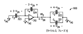
そうでない場合、クロック信号の第2のサイクルの第1のフェーズにおいて、図6の増幅構成600を介し、さらなる増幅を行うことができる。増幅構成600では、キャパシタ323の第1の端子および第2の端子は、それぞれ電圧基準VAGおよび増幅器312のマイナス入力端子に接続している。キャパシタ324の第1の端子および第2の端子は、それぞれ増幅器312の出力端子およびマイナス入力端子に接続している。増幅器312のプラス入力端子は電圧基準VAGに接続している。キャパシタ321の第1の端子およびキャパシタ322の第1の端子は増幅器312の出力端子に接続し、キャパシタ321の第2の端子およびキャパシタ322の第2の端子は電圧基準VAGに接続している。従って、増幅構成500と増幅構成600との間では、キャパシタ321およびキャパシタ323の場所が有効に入れ替わっており、キャパシタ322およびキャパシタ324の場所が有効に入れ替わっていることが分かる。
Otherwise, further amplification can be performed via the
増幅構成600では、キャパシタ323,324は、キャパシタ323,324の実質的な放電なく、スイッチング回路320を介して、図5の増幅構成500から再構成される。この構成では、増幅器312の出力電圧(VR2)が4×VIN(すなわち、2×2×VIN)であることが分かる。更に、この構成では、増幅器312の出力がキャパシタ321,322に電荷を生じさせるので、キャパシタ321,322の第1の端子と第2の端子との間の電圧差は、VR2、すなわち、4×VINに等しい。4X増幅が十分である場合、制御論理部308はアナログ部品306をRSD段に構成し、(キャパシタ321,322の端子間に存在する)増幅器312の出力電圧VR2を用いてRSD変換処理が開始される。
In
そうでない場合、クロック信号の第2のサイクルの第2のフェーズにおいて、図7の増幅構成700を介し、更なる増幅を行うことができる。増幅構成700のキャパシタ接続は増幅構成500のキャパシタ接続と同じであることが、図5と6の比較から分かる。しかし、増幅器構成700では、キャパシタ321,322は、キャパシタ321,322の実質的な放電なく、スイッチング回路320を介して図6の増幅構成600から再構成されるという違いがある。従って、増幅構成600と増幅構成700との間では、キャパシタ321およびキャパシタ323の場所が入れ替わっており、キャパシタ322およびキャパシタ324の場所が入れ替わっていることが分かる。この構成では、増幅器312の出力電圧(VR3)が8×VIN(すなわち、2×4×VIN)であることが分かる。更に、増幅器312の出力がキャパシタ323,324に電荷を生じさせるので、キャパシタ323,324の第1の端子と第2の端子との間の電圧差は、VR3、すなわち、8×VINと等しい。8X増幅が十分である場合、制御論理部308はアナログ部品306をRSD段に構成し、(キャパシタ321,322の端子間に存在する)増幅器312の出力電圧VR3を用いてRSD変換処理が開始される。
Otherwise, in the second phase of the second cycle of the clock signal, further amplification can be performed via the
8Xより大きい(且つ2の累乗である)増幅が必要な場合、所望の増幅に達するまで、増幅構成600と増幅構成700との間で交互に交替する構成のシーケンスを実行することができる。
If amplification greater than 8X (and a power of 2) is required, a sequence of configurations that alternate between
図4〜7に示すように、キャパシタ321〜324は、二つの対、すなわち、キャパシタ321,322を一方の対、キャパシタ323,324を別の対として編成されている。各増幅パスでは、第1の対のキャパシタが増幅構成に編成され、第2の対がサンプリング構成に編成される。その次の増幅パスでは、第2の対が(その蓄積された電荷の実質的な放電なく)増幅構成に再編成され、第1の対がサンプリング構成に再編成される。それに続く増幅パスでは、第1の対が(その蓄積された電荷の実質的な放電なく)増幅構成に再び編成され、第2の対がサンプリング構成に再編成される。以降も同様に増幅が反復される。従って、四つのキャパシタ321〜324が増幅段間で切り替えられる増幅反復のシーケンスを用いると、集積回路における実装に相当な空間を要する、大きなキャパシタネットワーク又は複雑な増幅回路を必要とすることなく、また、過剰な電力を無駄に消費することなく、2の累乗となる任意の様々な利得を実装できることが分かる。
4-7, the
図8には、本開示の少なくとも一つの実施形態による、図3のRSD ADC302の実装の一例を示す。スイッチング回路320は、トランジスタやパスゲートなどとして実装可能な、一組のスイッチ801〜809として設けられる。
FIG. 8 illustrates an example implementation of the
スイッチ801は、入力アナログ信号(VIN)を受信する第1の端子と、第2の端子とを含み、スイッチ制御信号SW5によって制御される。スイッチ802は、スイッチ801の第2の端子に接続した第1の端子と、増幅器312の出力に接続した第2の端子とを含み、スイッチ制御信号SW4によって制御される。スイッチ803は、スイッチ801の第2の端子に接続した第1の端子と、比較器332の入力に接続した第2の端子とを含み、スイッチ制御信号SW3によって制御される。スイッチ804は、増幅器312の出力に接続した第1の端子と、キャパシタ322の第1の端子に接続した第2の端子とを含み、スイッチ制御信号SW2によって制御される。スイッチ805は、スイッチ801の第2の端子に接続した第1の端子と、キャパシタ322の第1の端子に接続した第2の端子とを含み、スイッチ制御信号SW1によって制御される。スイッチ806は、スイッチ801の第2の端子に接続した第1の端子と、キャパシタ321の第1の端子に接続した第2の端子とを含み、スイッチ制御信号SW1によって制御される。スイッチ807は、電圧VREF+を受信する第1の端子と、キャパシタ321の第1の端子に接続した第2の端子とを含み、スイッチング信号h1によって制御される。スイッチ808は、電圧VREF−を受信する第1の端子と、キャパシタ321の第1の端子に接続した第2の端子とを含み、スイッチ制御信号l1によって制御される。スイッチ809は、キャパシタ321の第1の端子に接続した第1の端子と、電圧基準VAGに接続した第2の端子とを含み、スイッチ制御信号m1によって制御される。スイッチ810は、キャパシタ321の第2の端子およびキャパシタ322の第2の端子に接続した第1の端子と、増幅器312のマイナス入力に接続した第2の端子とを含み、スイッチ制御信号SW2によって制御される。スイッチ811は、キャパシタ321,322の第2の端子に接続した第1の端子と、電圧基準VAGに接続した第2の端子とを含み、スイッチ制御信号SW1によって制御される。スイッチ812は、増幅器312の出力に接続した第1の端子と、キャパシタ324の第1の端子に接続した第2の端子とを含み、スイッチ制御信号SW2によって制御される。スイッチ813は、増幅器312の出力に接続した第1の端子と、キャパシタ323の第1の端子に接続した第2の端子とを含み、スイッチ制御信号SW2によって制御される。スイッチ814は、キャパシタ324の第1の端子に接続した第1の端子と、増幅器312の出力に接続した第2の端子とを含み、スイッチ制御信号SW1によって制御される。スイッチ815は、電圧VREF+を受信する第1の端子と、キャパシタ323の第1の端子に接続した第2の端子とを含み、スイッチ制御信号h2によって制御される。スイッチ816は、電圧VREF−を受信する第1の端子と、キャパシタ323の第1の端子に接続した第2の端子とを含み、スイッチ制御信号l2によって制御される。スイッチ817は、キャパシタ323の第1の端子に接続した第1の端子と、電圧基準VAGに接続した第2の端子とを含み、スイッチ制御信号m2によって制御される。スイッチ818は、キャパシタ323の第2の端子およびキャパシタ324の第2の端子に接続した第1の端子と、増幅器312のマイナス入力に接続した第2の端子とを含み、スイッチ制御信号SW1によって制御される。スイッチ819は、キャパシタ323,324の第2の端子に接続した第1の端子と、電圧基準VAGに接続した第2の端子とを含み、スイッチ信号SW2によって制御される。
The
図示した例では、制御論理部308は、クロック信号(CLK)を受信するための入力と、比較器332の出力に結合した入力と、比較器334の出力に結合した入力とを含むと共に、クロック信号および比較器332,334の出力した値に基づいてスイッチ制御信号SW1〜SW5,h1,h2,l1,l2,m1,m2を提供する出力を含んでいる。
In the illustrated example, the
下記のテーブル1は、図4の初期サンプリング構成400と図5,6,7の増幅構成500,600,700とを編成するために制御論理部308が設定するスイッチ制御信号の様々な状態を示す。テーブル1では、“0”,“1”の値は対応するスイッチをそれぞれ“開”(すなわち、非導通)状態、“閉”(すなわち、導通)状態にそれぞれ設定し、“X”は“管理せず”の状態であると仮定する。
テーブル1:変換前の増幅のためのスイッチ制御信号の設定
Table 1 below shows the various states of the switch control signals set by the
Table 1: Switch control signal settings for amplification before conversion

テーブル1によって示すように、制御論理部308では、CLK信号(図3)のクロックサイクルのフェーズに基づいて異なる構成を実装できる。更に、テーブル1によって示すように、スイッチ制御信号SW1およびスイッチ制御信号SW2は、相補信号として設けることができる。
As shown by Table 1, the
下記のテーブル2は、増幅された入力信号の変換用のRSD構成を編成するために制御論理部308が設定するスイッチ制御信号の様々な状態を示す。テーブル2では、サンプリング構成400、増幅構成500、増幅構成600のシーケンスを介して達成された4X増幅が所望の利得であるため、RSD構成は増幅構成600から開始されると仮定する。更に、テーブル2では最初の四つのRSDサイクルのみを示すが、RSDサイクルの総数は特定の実装の解に応じてよいことが分かる。テーブル2では、“0”,“1”の値は対応するスイッチをそれぞれ“開”(すなわち、非導通)状態、“閉”(すなわち、導通)状態にそれぞれ設定し、“X”は“管理なし”の状態であり、スイッチ制御信号h1,l1,m1,h2,l2,m2の“D”は、対応する信号の状態がVH,VLと比較して解析される残留電圧の電圧に依存することを示す(すなわち、比較器332,334の出力した値に依存して残留電圧をオフセットする(VR±VREF))。
テーブル2: RSD変換のためのスイッチ制御信号の設定
Table 2 below shows the various states of the switch control signal set by the
Table 2: Setting of switch control signal for RSD conversion
図9は、本開示の少なくとも一つの実施形態による、RSD ADCの差動送信方式の実装の一例を示す。図示したRSD ADC902(図1のRSD ADC102に相当)は、アナログ部品906と、制御論理部908と、デジタル変換論理部(図示せず)とを含んでいる。アナログ部品906は、差動増幅器912と、キャパシタネットワーク914とを含み、キャパシタネットワーク914は、スイッチング回路920と、四つのキャパシタ921,922,923,924(まとめて、キャパシタ921〜924)のような複数のキャパシタとを備える。スイッチング回路920は、複数のスイッチと、差動増幅器912の入力端子(例えば、マイナス(−)入力端子)に接続した端子と、差動増幅器912のプラス(+)出力端子に接続した端子とを含んでいる。スイッチング回路920は、差動入力アナログ信号の一方の成分(例えば、VIN+)と、一つ又は複数の基準電圧(例えば、VREF+,VREF−)と、複数のスイッチ制御信号SW1〜SWnとを受信するための入力を更に含んでいる。スイッチ制御信号SW1〜SWnは、キャパシタ921〜924の様々な構成に影響を与えるようにスイッチに対し送られる。スイッチング回路920は、差動出力信号の一つの成分をデジタル変換論理部(図示せず)に提供する出力を更に備え、ここで、第1の成分は、RSD ADC902の動作の特定の段に応じて、成分VIN+、成分VIN+の増幅されたもの、又は差動残留電圧の成分(例えば、VR+)のいずれかを含む。
FIG. 9 illustrates an example implementation of a differential transmission scheme for an RSD ADC according to at least one embodiment of the present disclosure. The illustrated RSD ADC 902 (corresponding to the
アナログ部品906は、差動入力アナログ信号の第2の成分(例えば、VIN−)のためのキャパシタネットワーク915を更に含んでいる。キャパシタネットワーク915は、スイッチング回路919(スイッチング回路920に相当)と、四つのキャパシタ925,926,927,928(まとめて、キャパシタ925〜928)のような複数のキャパシタとを備えている。スイッチング回路919は、複数のスイッチと、差動増幅器912の他方の入力端子(例えば、プラス(+)入力端子)に接続した端子と、差動増幅器912のマイナス(−)出力端子に接続した端子とを含んでいる。スイッチング回路919は、差動入力アナログ信号の他方の成分(例えば、VIN−)と、一つ又は複数の基準電圧(例えば、VREF+,VREF−)と、複数のスイッチ制御信号SWn+1〜SWmとを受信するための入力を更に含んでいる。スイッチ制御信号は、キャパシタ925〜928の様々な構成に影響を与えるように、スイッチング回路919のスイッチに対し送られる。スイッチング回路919は、差動出力信号の第2の成分を提供する出力を更に備え、ここで、第2の成分は、RSD ADC902の動作の特定の段に応じて、成分VIN−、成分VIN−の増幅されたもの、又は差動残留電圧の成分(例えば、VR−)のいずれかを含む。キャパシタネットワーク914,915は、各々、シングルエンド型の実装について上述した図8の例と同様な方式で実装できる。
制御論理部908は、一つ又は複数のクロック信号(CLK)を受信するための入力と、イネーブル(EN)信号およびスイッチ制御信号SW1〜SWmを提供する出力とを含んでいる。少なくとも一つの実施形態において、制御論理部908は、スイッチング回路919,920を介してキャパシタ921〜928の様々な構成に影響を与えると共に一つ又は複数のクロック信号のフェーズに基づいてデジタル変換論理部を作動可能又は作動不能にするように、スイッチ制御信号およびEN信号を構成する。
The
少なくとも一つの実施形態では、図9の差動送信方式の実装は、シングルエンド型の入力アナログ信号に使用できる。この例で、シングルエンド型の入力アナログ信号VINが第1の成分VIN+として提供され、電圧基準VAGが第2の成分VIN−として供給される。従って、RSD ADC902は、増幅および変換の前に、シングルエンド型の入力アナログ信号を差動信号に変換する、更なる特徴を有する。
In at least one embodiment, the differential transmission scheme implementation of FIG. 9 can be used for single-ended input analog signals. In this example, a single-ended input analog signal VIN is provided as a first component V IN + and a voltage reference V AG is provided as a second component V IN− . Thus,
少なくとも一つの実施形態では、制御論理部908は、上述の図3の状態図340のものと同様な動作を有するハードウェア状態機械を実装する。図3のシングルエンド型の実装の制御論理部308の場合のように、差動信号方式の実装の制御論理部908は、入力アナログ信号(入力における真の差動信号か、差動信号に変換されたシングルエンド型の信号のいずれか)を漸増させるための一つ又は複数の増幅パスを得るように、キャパシタ921〜928を様々な構成に編成する。
In at least one embodiment,
図10〜12は、本開示の少なくとも一つの実施形態による、差動入力信号の特定の増幅を達成するために利用できるキャパシタ構成のシーケンスを示す。簡単な図解とするために、キャパシタ構成のシーケンスは、図9のRSD ADC902に関連して説明される。図示した構成はスイッチング回路920およびスイッチング回路919のスイッチの構成を介して達成されるが、明確にするために、スイッチは図10〜12に図示した構成から省略されている。
10-12 illustrate a sequence of capacitor configurations that can be utilized to achieve specific amplification of a differential input signal, according to at least one embodiment of the present disclosure. For the sake of simplicity, the capacitor configuration sequence is described in connection with the
図10は、クロック信号の第1のサイクルの第1のフェーズにおける、キャパシタ921,922,925,926(C1,C2,C5,C6)からなる初期サンプリング構成1000を示す。キャパシタ921の第1の端子およびキャパシタ922の第1の端子は、電圧VIN+を受信するように入力アナログ電圧の第1の成分に接続している。キャパシタ921の第2の端子およびキャパシタ922の第2の端子は電圧基準VAGに接続している。同様に、キャパシタ925の第1の端子およびキャパシタ926の第1の端子は、電圧VIN−を受信するように入力アナログ電圧の第2の成分に接続し、キャパシタ925の第2の端子およびキャパシタ926の第2の端子は、電圧基準VAGに接続している。図10によって示すように、初期サンプリング構成1000は、キャパシタ921,922の各々に加わる電圧VIN+と、キャパシタ925,926の各々に加わる電圧VIN−とを生じる。
FIG. 10 shows an
図11は、クロック信号の第1のサイクルの第2のフェーズにおける、キャパシタ921〜928からなる増幅構成1100を示す。キャパシタ921の第1の端子および第2の端子は、それぞれ電圧基準VAGおよび差動増幅器912のマイナス入力端子に接続している。キャパシタ922の第1の端子および第2の端子は、それぞれ差動増幅器912のプラス出力端子およびマイナス入力端子に接続している。キャパシタ925の第1の端子および第2の端子は、それぞれ電圧基準VAGおよび差動増幅器912のプラス入力端子に接続している。キャパシタ926の第1の端子および第2の端子は、それぞれ差動増幅器912のマイナス出力端子およびプラス入力端子に接続している。キャパシタ923の第1の端子およびキャパシタ924の第1の端子は差動増幅器912のプラス出力端子に接続し、キャパシタ923の第2の端子およびキャパシタ924の第2の端子は電圧基準VAGに接続している。キャパシタ927の第1の端子およびキャパシタ928の第1の端子は差動増幅器912のマイナス出力端子に接続し、キャパシタ927の第2の端子およびキャパシタ928の第2の端子は電圧基準VAGに接続している。
FIG. 11 shows an
増幅構成1100では、キャパシタ921,922は、キャパシタ921,922を放電することなく、スイッチング回路920を介して図10の初期サンプリング構成1000から再構成される。同様に、キャパシタ925,926は、キャパシタ925,926を放電することなく、スイッチング回路919を介して図10の初期サンプリング構成1000から再構成される。この構成では、差動増幅器の出力電圧(VR1+−VR1−)は2×(VIN+−VIN−)であることが分かる。
In the
更に、増幅構成1100では、差動増幅器912のプラス出力端子がキャパシタ923,924に電荷を生じさせるので、キャパシタ923,924の第1の端子と第2の端子との間の電圧差は、VR1+、すなわち、2×VIN+に等しくなる。差動増幅器912のマイナス出力端子がキャパシタ927,928に電荷を生じさせるので、キャパシタ927,928の第1の端子と第2の端子との間の電圧差は、VR1−、すなわち、2×VIN−に等しくなる。2X増幅が十分である場合、アナログ部品906がRSD変換構成に編成され、(キャパシタ323,324およびキャパシタ327,328の端子間電圧で表される)2X増幅されたアナログ信号を用いて変換処理が開始される。
Further, in the
そうでない場合、クロック信号の第2のサイクルの第1のフェーズにおいて、図12の増幅構成1200を介し、さらなる増幅を行うことができる。増幅構成1200では、キャパシタ923の第1の端子および第2の端子は、それぞれ電圧基準VAGおよび差動増幅器912のマイナス入力端子に接続している。同様に、キャパシタ927の第1の端子および第2の端子は、それぞれ電圧基準VAGおよび差動増幅器912のプラス入力端子に接続している。キャパシタ924の第1の端子および第2の端子は、それぞれ差動増幅器912のプラス出力端子およびマイナス入力端子に接続している。キャパシタ928の第1の端子および第2の端子は、それぞれ差動増幅器912のマイナス出力端子およびプラス入力端子に接続している。キャパシタ921の第1の端子およびキャパシタ922の第1の端子は差動増幅器912のプラス出力端子に接続し、キャパシタ921の第2の端子およびキャパシタ922の第2の端子は電圧基準VAGに接続している。キャパシタ925の第1の端子およびキャパシタ926の第1の端子は差動増幅器912のマイナス出力端子に接続し、キャパシタ925の第2の端子およびキャパシタ926の第2の端子は電圧基準VAGに接続している。従って、増幅構成1100と増幅構成1200の間では、キャパシタ921およびキャパシタ923の場所が入れ替わっており、キャパシタ922およびキャパシタ924の場所が入れ替わっており、キャパシタ925およびキャパシタ927の場所が入れ替わっており、キャパシタ926およびキャパシタ928の場所が入れ替わっていることが分かる。
Otherwise, in the first phase of the second cycle of the clock signal, further amplification can be performed via the
増幅構成1200では、キャパシタ923,924,927,928は、キャパシタ923,924,927,928を放電することなく、スイッチング回路919およびスイッチング回路920を介して図11の増幅構成1100から再構成される。この構成では、差動増幅器912の出力電圧(VR+2−VR−2)は4×(VIN+−VIN− )、すなわち、2×2×(VIN+−VIN− )であることが分かる。
In
更に、差動増幅器912のプラス出力がキャパシタ921,922に電荷を生じさせるので、キャパシタ921,922の第1の端子と第2の端子との間の電圧差は、VR+2、すなわち、4×VIN+と等しくなる。差動増幅器912のマイナス出力がキャパシタ925,926に電荷を生じさせるので、キャパシタ925,926の第1の端子と第2の端子との間の電圧差は、VR−2、すなわち、4×VIN−と等しくなる。4X増幅が十分である場合、4X増幅されたアナログ信号を用いて変換処理が開始される。そうではなく、4Xより大きい(且つ2の累乗である)増幅が必要な場合、所望の増幅に達成するまで、増幅構成1100と増幅構成1200との間で交互に交替する構成のシーケンスを実行することができる。
Further, since the positive output of the
図13〜15は、本明細書に記載の技術による、デジタル変換用にシングルエンド型の入力信号を差動信号に変換するキャパシタ構成のシーケンスの例を示す。図13,14の組み合わせは、シングルエンド型の入力信号を増幅せずに差動信号に変換するキャパシタ構成のシーケンスを示す。図13,15の組み合わせは、シングルエンド型の入力信号を差動信号に変換するとともに、得られる差動信号において2X利得を得るキャパシタ構成のシーケンスを示す。簡単な説明とするために、キャパシタ構成のシーケンスは、図9のRSD ADC902に関連して説明される。図示した構成はスイッチング回路920およびスイッチング回路919のスイッチからなる構成から達成されるが、明確にするために、スイッチは図13〜15に図示した構成から省略されている。
FIGS. 13-15 show examples of capacitor configuration sequences for converting single-ended input signals to differential signals for digital conversion in accordance with the techniques described herein. The combination of FIGS. 13 and 14 shows a capacitor configuration sequence for converting a single-ended input signal into a differential signal without amplification. The combination of FIGS. 13 and 15 shows a capacitor configuration sequence for converting a single-ended input signal into a differential signal and obtaining 2 × gain in the obtained differential signal. For the sake of brevity, the capacitor configuration sequence is described in connection with the
図13は、クロック信号の第1のサイクルの第1のフェーズにおける、キャパシタ921,925からなる初期サンプリング構成1300を示す。キャパシタ921の第1の端子はシングルエンド型の入力信号のアナログ電圧VINを受信するように接続し、キャパシタ925の第1の端子は電圧基準VAGに接続している。キャパシタ921の第2の端子およびキャパシタ925の第2の端子は、電圧基準VAGに接続している。更に、キャパシタ922,926は、キャパシタ925と同じ方式で構成されている。したがって、初期サンプリング構成1300は、キャパシタ921に加わる電圧VX(ここで、VX=VIN−VAG)と、キャパシタ922,925,926に加わる約0Vの電圧とを生じる。
FIG. 13 shows an
図14は、クロック信号の第1のサイクルの第2のフェーズにおける、キャパシタ921〜928からなる差動信号変換構成1400に対する増幅されないシングルエンド型の信号を示す。キャパシタ921の第1の端子および第2の端子は、それぞれ電圧基準VAGおよび差動増幅器912のマイナス入力端子に接続している。キャパシタ922の第1の端子および第2の端子は、それぞれ差動増幅器912のプラス出力端子およびマイナス入力端子に接続している。キャパシタ925の第1の端子および第2の端子は、それぞれ電圧基準VAGおよび差動増幅器912のプラス入力端子に接続している。キャパシタ926の第1の端子および第2の端子は、それぞれ差動増幅器912のマイナス出力端子およびプラス入力端子に接続している。キャパシタ923の第1の端子およびキャパシタ924の第1の端子は差動増幅器912のプラス出力端子に接続し、キャパシタ923の第2の端子およびキャパシタ924の第2の端子は電圧基準VAGに接続している。キャパシタ927の第1の端子およびキャパシタ928の第1の端子は差動増幅器912のマイナス出力端子に接続し、キャパシタ927の第2の端子およびキャパシタ928の第2の端子は電圧基準VAGに接続している。
FIG. 14 shows an unamplified single-ended signal for the differential
この構成では、差動増幅器912の出力電圧がVXであるため、電圧VINを有するシングルエンド型の出力信号が信号成分間に電圧差VXを有する差動信号に変換されることが分かる。得られる差動信号は、次いで、キャパシタ923,924,927,928によってサンプリングされ、上述のように増幅およびデジタル変換処理される。
In this configuration, since the output voltage of the
図15は、クロック信号の第1のサイクルの第2のフェーズにおける、キャパシタ921〜928からなる、代替のシングルエンド型の差動変換構成1500を示しており、ここで、得られる信号はシングルエンド型から差動信号に変換されると共に、2Xの利得だけ増幅されている。図15の構成1500は、キャパシタ925の第1の端子が(図14の構成1400におけるように電圧基準VAGに接続しているのではなく)シングルエンド型の入力信号の電圧VINを受信するように接続していることを除き、図14の構成1400と同じである。この構成では、差動増幅器912の出力電圧は2×VXであるため、電圧VINを有するシングルエンド型の入力信号が信号成分間に電圧差2×VXを有する差動信号に変換および増幅されることが分かる。得られる差動信号は、次いで、キャパシタ923,924,927,928によってサンプリングされ、上述のようにサンプリングキャパシタを介して増幅およびデジタル変換処理される。
FIG. 15 shows an alternative single-ended
図16は、本開示の少なくとも一つの実施形態による、RSD ADCの実装の別の例を示す。上述の実施形態では、スイッチング回路は、所望の電圧レベルまで入力アナログ信号を反復的に増幅するように、多増幅パス用の様々なキャパシタ構成を編成するために用いられている。図16に示すRSD ADC1602は、キャパシタ1621,1622に代えて、プログラム可能なキャパシタ1621,1622を用いることと、制御論理部1608が、プログラム可能なキャパシタ1621,1622の静電容量をそれぞれ調整する静電容量調整信号CAP1,CAP2も提供するように構成されることとを除き、図8に示したRSD ADC302とほぼ同様である。一実施形態では、プログラム可能なキャパシタ1621,1622は、プログラム可能キャパシタのネットワークとして構成され、その例は上述の米国特許第5,625,361号明細書に記載されている。図16はシングルエンド型の実装を示しているが、図9に示したのと同様に、プログラム可能キャパシタベースのRSD ADCは差動送信方式の実装として実装できる。
FIG. 16 illustrates another example of an RSD ADC implementation in accordance with at least one embodiment of the present disclosure. In the embodiments described above, the switching circuit is used to organize various capacitor configurations for multiple amplification paths so as to repeatedly amplify the input analog signal to a desired voltage level. The
図17は、本開示の少なくとも一つの実施形態による、図16のRSD ADC1602の動作の方法1700の一例を示す。少なくとも一つの実施形態では、方法1700は、少なくとも部分的には制御論理部1608の状態機械として実装される。
FIG. 17 illustrates an
ブロック1702にて、制御論理部1608は、増幅器312を含む増幅器構成に構成されると入力アナログ信号の所望の増幅を提供するように、プログラム可能キャパシタ1621,1622の静電容量を構成する。プログラム可能なキャパシタ1621がプログラム可能な静電容量C1を有し、プログラム可能なキャパシタ1622がプログラム可能な静電容量C2を有すると仮定すると、この構成の増幅器312の出力電圧(VR)は、次式と等しくなる。
At
従って、増幅器312とプログラム可能なキャパシタ1621,1622とからなる増幅構成の利得(Gain)は、次式で表される。
Therefore, the gain (Gain) of the amplification configuration including the
特定の利得を得るために、制御論理部1608は、特別の利得に対応する静電容量C2対静電容量C1の比を得るように、信号CAP1,CAP2を介して静電容量C1,C2を調整できる。例えば、2X利得を得るために、制御論理部308は、プログラム可能なキャパシタ1621,1622が実質的に同様の静電容量を有する(すなわち、静電容量C2対静電容量C1の比が1:1であり、2の利得を生じる)ように、ブロック1702にてプログラム可能なキャパシタ1621,1622をプログラムできる。同様に、3Xの利得を得るために、プログラム可能なキャパシタ1622の静電容量C1は、プログラム可能なキャパシタ1621の静電容量C2の1/2に設定できる(すなわち、静電容量C2対静電容量C1の比が2:1になり、3の利得を生じる)。更に、4Xの利得を得るために、プログラム可能なキャパシタ1622の静電容量C1は、プログラム可能なキャパシタ1621の静電容量C2の1/3に設定できる(すなわち、静電容量C2対静電容量C1の比が3:1になり、4の利得を生じる)。静電容量の所望の比は、RSD変換段中に用いられる静電容量に静電容量C1を維持しつつ静電容量C2を増加させることにより、RSD変換段中に用いられる静電容量に静電容量C2を維持しつつ静電容量C1を減少させることにより、又は静電容量C1を減少させつつ静電容量C2を増加させることにより、得ることができる。
In order to obtain a specific gain, the
プログラム可能キャパシタ1621,1622を所望の静電容量にプログラムした後、プログラム可能キャパシタ1621,1622は、図4の初期サンプリング構成400に相当する初期サンプリング構成に構成される。この構成において、入力アナログ信号は、入力アナログ信号の電圧VINと等しい電圧差をそれらのキャパシタの端子間に生じるように、プログラム可能キャパシタ1621,1622に対し印加される。
After programming
プログラム可能キャパシタ1621,1622を用いて入力アナログ信号をサンプリングした後、ブロック1704にて、プログラム可能キャパシタ1621,1622およびキャパシタ1623,1624は、入力アナログ信号を増幅し、増幅されたアナログ信号を生成するように、図5の増幅構成500に相当する増幅器構成に構成される。上述のように、得られる増幅された信号の利得は、1+(C2/C1)とほぼ等しくなる。
After sampling the input analog signal using
ブロック1706にて、スイッチ801〜819は、増幅されたアナログ信号をデジタル信号に変換するために、プログラム可能キャパシタ1621,1622およびキャパシタ1623,1624を従来のRSDアナログ段に再構成するように切り替えられる。この再構成には、例えば、実質的に等しい静電容量を有するように、プログラム可能キャパシタ1621,1622を再プログラムすることによって、変換処理中に2Xの標準利得を有するようにRSDアナログ段を構成することが含まれてよい。
At
本明細書において用いた用語“別の”は、少なくとも第2の又はそれ以上の、と定義される。本明細書において用いた用語“備える”、“有する”、又は、その任意の変形は、含む、と定義される。本明細書において光電気技術に関連して用いた用語“結合した”は、接続した、と定義されるが、必ずしも直接的でも、機械的でもない。 As used herein, the term “another” is defined as at least a second or more. The terms “comprising”, “having”, or any variation thereof, as used herein, are defined to include. The term “coupled” as used herein in connection with optoelectronic technology is defined as connected, but is not necessarily direct or mechanical.
本開示の他の実施形態、使用、および利点は、本明細書の詳細な説明および実施例を考慮すると、当業者には明らかである。明細書および図面は例示として考慮されるものに過ぎず、したがって、本開示の範囲は、添付の特許請求の範囲およびその均等によってのみ限定されることを意図するものである。 Other embodiments, uses, and advantages of the present disclosure will be apparent to those skilled in the art in view of the detailed description and examples herein. The specification and drawings are to be considered merely as exemplary and therefore the scope of the present disclosure is intended to be limited only by the appended claims and equivalents thereof.
Claims (8)
第1のアナログ信号を受信する第1の入力端子と、
第1の入力端子に結合したアナログ部品であって、
第1の入力と第1の出力とを備える増幅器と、
増幅器の第1の入力と第1の出力とに結合しており、複数のキャパシタを含む第1のキャパシタネットワークと、を備える、アナログ部品と、
制御論理部と、を備え、制御論理部は、
第1のモードでは、第1のアナログ信号を所定の利得によって増幅して第1の増幅されたアナログ信号を生成する増幅構成に、増幅器および第1のキャパシタネットワークを構成し、
第2のモードでは、第1の増幅されたアナログ信号を用いて一つ又は複数の残留電圧からなる第1の一連の残留電圧を生成するように、増幅器および第1のキャパシタネットワークを構成するように構成されており、
前記第1のキャパシタネットワークは、
第1の入力端子に結合可能かつ電圧基準に結合可能な第1の端子と、増幅器の第1の入力に結合可能かつ電圧基準に結合可能な第2の端子とを備える、第1のキャパシタと、
第1の入力端子に結合可能かつ増幅器の第1の出力に結合可能な第1の端子と、増幅器の第1の入力に結合可能かつ電圧基準に結合可能な第2の端子とを備える、第2のキャパシタと、
増幅器の第1の出力に結合可能かつ電圧基準に結合可能な第1の端子と、増幅器の第1の入力に結合可能かつ電圧基準に結合可能な第2の端子とを備える、第3のキャパシタと、
増幅器の第1の出力に結合可能かつ電圧基準に結合可能な第1の端子と、増幅器の第1の入力に結合可能かつ電圧基準に結合可能な第2の端子とを備える、第4のキャパシタと、を備えるアナログ−デジタル変換器(ADC)デバイス。 In an analog-to-digital converter (ADC) device:
A first input terminal for receiving a first analog signal;
An analog component coupled to the first input terminal,
An amplifier comprising a first input and a first output;
An analog component comprising: a first capacitor network coupled to a first input and a first output of the amplifier and including a plurality of capacitors;
A control logic unit, and the control logic unit includes:
In the first mode, the amplifier and the first capacitor network are configured in an amplification configuration that amplifies the first analog signal by a predetermined gain to generate a first amplified analog signal;
In the second mode, the amplifier and the first capacitor network are configured to generate a first series of residual voltages comprising one or more residual voltages using the first amplified analog signal. Is composed of
The first capacitor network includes:
A first capacitor comprising: a first terminal coupleable to a first input terminal and coupleable to a voltage reference; and a second terminal coupleable to a first input of the amplifier and coupleable to a voltage reference; ,
A first terminal coupleable to a first input terminal and coupleable to a first output of the amplifier, and a second terminal coupleable to a first input of the amplifier and coupleable to a voltage reference; Two capacitors;
A third capacitor comprising a first terminal coupleable to a first output of the amplifier and coupleable to a voltage reference, and a second terminal coupleable to the first input of the amplifier and coupleable to a voltage reference When,
A fourth capacitor comprising a first terminal coupleable to a first output of the amplifier and coupleable to a voltage reference; and a second terminal coupleable to a first input of the amplifier and coupleable to a voltage reference An analog-to-digital converter (ADC) device.
第1のアナログ信号を受信する第1の入力端子と、
第1の入力端子に結合したアナログ部品であって、
第1の入力と第1の出力とを備える増幅器と、
増幅器の第1の入力と第1の出力とに結合しており、複数のキャパシタを含む第1のキャパシタネットワークと、を備える、アナログ部品と、
制御論理部と、を備え、制御論理部は、
第1のモードでは、第1のアナログ信号を所定の利得によって増幅して第1の増幅されたアナログ信号を生成する増幅構成に、増幅器および第1のキャパシタネットワークを構成し、
第2のモードでは、第1の増幅されたアナログ信号を用いて一つ又は複数の残留電圧からなる第1の一連の残留電圧を生成するように、増幅器および第1のキャパシタネットワークを構成するように構成されており、
第1のキャパシタネットワークは、
第1の入力端子に結合可能かつ電圧基準に結合可能な第1の端子と、増幅器の第1の入力に結合可能かつ電圧基準に結合可能な第2の端子とを備える、第1のプログラム可能キャパシタと、
第1の入力端子に結合可能かつ増幅器の第1の出力に結合可能な第1の端子と、増幅器の第1の入力に結合可能かつ電圧基準に結合可能な第2の端子とを備える、第2のプログラム可能キャパシタと、
増幅器の第1の出力に結合可能かつ電圧基準に結合可能な第1の端子と、増幅器の第1の入力に結合可能かつ電圧基準に結合可能な第2の端子とを備える、第3のキャパシタと、
増幅器の第1の出力に結合可能かつ電圧基準に結合可能な第1の端子と、増幅器の第1の入力に結合可能かつ電圧基準に結合可能な第2の端子とを備える、第4のキャパシタと、を備えるアナログ−デジタル変換器(ADC)デバイス。 In an analog-to-digital converter (ADC) device:
A first input terminal for receiving a first analog signal;
An analog component coupled to the first input terminal,
An amplifier comprising a first input and a first output;
An analog component comprising: a first capacitor network coupled to a first input and a first output of the amplifier and including a plurality of capacitors;
A control logic unit, and the control logic unit includes:
In the first mode, the amplifier and the first capacitor network are configured in an amplification configuration that amplifies the first analog signal by a predetermined gain to generate a first amplified analog signal;
In the second mode, the amplifier and the first capacitor network are configured to generate a first series of residual voltages comprising one or more residual voltages using the first amplified analog signal. Is composed of
The first capacitor network is
A first programmable device comprising a first terminal coupleable to a first input terminal and coupleable to a voltage reference, and a second terminal coupleable to a first input of the amplifier and coupleable to a voltage reference A capacitor;
A first terminal coupleable to a first input terminal and coupleable to a first output of the amplifier, and a second terminal coupleable to a first input of the amplifier and coupleable to a voltage reference; Two programmable capacitors;
A third capacitor comprising a first terminal coupleable to a first output of the amplifier and coupleable to a voltage reference, and a second terminal coupleable to the first input of the amplifier and coupleable to a voltage reference When,
A fourth capacitor comprising a first terminal coupleable to a first output of the amplifier and coupleable to a voltage reference; and a second terminal coupleable to a first input of the amplifier and coupleable to a voltage reference An analog-to-digital converter (ADC) device.
所定の利得に基づいて、第1のプログラム可能キャパシタを第1の静電容量に構成し、第2のプログラム可能キャパシタを第2の静電容量に構成し、
第1のフェーズにて、第1のプログラム可能キャパシタの第1の端子および第2のプログラム可能キャパシタの第1の端子を第1の入力端子に結合するように、かつ、第1のプログラム可能キャパシタの第2の端子および第2のプログラム可能キャパシタの第2の端子を電圧基準に結合するように、キャパシタネットワークを構成し、
第1のフェーズに続く第2のフェーズにて、第1のプログラム可能キャパシタの第1の端子を電圧基準に結合し、第1のプログラム可能キャパシタの第2の端子を増幅器の第1の入力に結合し、第2のプログラム可能キャパシタの第1の端子を増幅器の第1の出力に結合し、第2のプログラム可能キャパシタの第2の端子を増幅器の第1の入力に結合するように、キャパシタネットワークを構成するように構成されている、請求項2に記載のADCデバイス。 The control logic unit is in the first mode:
Based on the predetermined gain, configuring the first programmable capacitor to a first capacitance, configuring the second programmable capacitor to a second capacitance,
Coupling the first terminal of the first programmable capacitor and the first terminal of the second programmable capacitor to the first input terminal in the first phase and the first programmable capacitor; Configuring a capacitor network to couple the second terminal of the second and the second terminal of the second programmable capacitor to a voltage reference;
In a second phase following the first phase, the first terminal of the first programmable capacitor is coupled to a voltage reference, and the second terminal of the first programmable capacitor is the first input of the amplifier. A capacitor coupled to couple the first terminal of the second programmable capacitor to the first output of the amplifier and to couple the second terminal of the second programmable capacitor to the first input of the amplifier. The ADC device according to claim 2, wherein the ADC device is configured to form a network.
第2のモードにおいて、第1のプログラム可能キャパシタを第3の静電容量に構成し、第2のプログラム可能キャパシタを第3の静電容量に構成するように構成されている、請求項3に記載のADCデバイス。 The control logic is
4. In the second mode, the first programmable capacitor is configured to a third capacitance, and the second programmable capacitor is configured to a third capacitance. The described ADC device.
増幅器は、第1の入力、第2の入力、第1の出力、および第2の出力を備える、差動増幅器を含み、
アナログ部品は、前記増幅器の第2の入力と第2の出力とに結合しており複数のキャパシタを含む第2のキャパシタネットワークを更に備え、
制御論理部は、
第1のモードでは、第2のアナログ信号を前記所定の利得によって増幅して第2の増幅されたアナログ信号を生成する増幅構成に、増幅器および第2のキャパシタネットワークを構成し、
第2のモードでは、第2の増幅されたアナログ信号を用いて一つ又は複数の残留電圧からなる第2の一連の残留電圧を生成するように、増幅器および第2のキャパシタネットワークを構成するように構成されている、請求項1又は2に記載のADCデバイス。 A second input terminal for receiving a second analog signal;
The amplifier includes a differential amplifier comprising a first input, a second input, a first output, and a second output;
The analog component further comprises a second capacitor network coupled to the second input and the second output of the amplifier and including a plurality of capacitors,
The control logic is
In the first mode, an amplifier and a second capacitor network are configured in an amplification configuration for amplifying a second analog signal by the predetermined gain to generate a second amplified analog signal;
In the second mode, the amplifier and the second capacitor network are configured to generate a second series of residual voltages comprising one or more residual voltages using the second amplified analog signal. The ADC device according to claim 1, wherein the ADC device is configured as follows.
第1のアナログ信号を第1の利得によって増幅して第1の増幅されたアナログ信号を生成するように、ADCの増幅器および第1のキャパシタネットワークを構成する工程と、
第1の増幅されたアナログ信号に基づいて一つ又は複数の残留電圧からなる第1の一連の残留電圧を生成するように、増幅器および第1のキャパシタネットワークを構成する工程と、
ADCからの出力のために一つ又は複数の残留電圧からなる第1の一連の残留電圧に基づいてデジタル値を提供する工程と、を備え、
第1のアナログ信号を増幅するように、増幅器および第1のキャパシタネットワークを構成する工程は、
第1の利得に基づいて、第1の静電容量を有するように第1のキャパシタネットワークの第1のプログラム可能キャパシタを構成し、第2の静電容量を有するように第1のキャパシタネットワークの第2のプログラム可能キャパシタを構成する工程と、
第1のフェーズにて、
第1のプログラム可能キャパシタの第1の端子および第2のプログラム可能キャパシタの第1の端子を第1の入力端子に結合する工程と、
第1のプログラム可能キャパシタの第2の端子および第2のプログラム可能キャパシタの第2の端子を電圧基準に結合する工程と、 第1のフェーズに続く第2のフェーズにて、
第1のプログラム可能キャパシタの第2の端子および第2のプログラム可能キャパシタの第2の端子を増幅器の入力に結合する工程と、
第1のプログラム可能キャパシタの第1の端子を電圧基準に結合する工程と、
第2のプログラム可能キャパシタの第1の端子を増幅器の出力に結合する工程と、
第1のキャパシタネットワークにおける第3のキャパシタの第1の端子および第1のキャパシタネットワークにおける第4のキャパシタの第1の端子を増幅器の出力に結合する工程と、
第3のキャパシタの第2の端子および第4のキャパシタの第2の端子を電圧基準に結合する工程と、を含む方法。 Receiving a first analog signal at a first input terminal of an analog-to-digital converter (ADC);
Configuring the amplifier of the ADC and the first capacitor network to amplify the first analog signal by a first gain to produce a first amplified analog signal;
Configuring the amplifier and the first capacitor network to generate a first series of residual voltages comprising one or more residual voltages based on the first amplified analog signal;
Providing a digital value based on a first series of residual voltages comprising one or more residual voltages for output from the ADC,
Configuring the amplifier and the first capacitor network to amplify the first analog signal comprises:
Based on the first gain, the first programmable capacitor of the first capacitor network is configured to have a first capacitance, and the first capacitor network is configured to have a second capacitance. Configuring a second programmable capacitor;
In the first phase,
Coupling the first terminal of the first programmable capacitor and the first terminal of the second programmable capacitor to the first input terminal;
Coupling the second terminal of the first programmable capacitor and the second terminal of the second programmable capacitor to a voltage reference; in a second phase following the first phase;
Coupling the second terminal of the first programmable capacitor and the second terminal of the second programmable capacitor to the input of the amplifier;
Coupling the first terminal of the first programmable capacitor to a voltage reference;
Coupling the first terminal of the second programmable capacitor to the output of the amplifier;
Coupling a first terminal of a third capacitor in the first capacitor network and a first terminal of a fourth capacitor in the first capacitor network to the output of the amplifier;
Coupling the second terminal of the third capacitor and the second terminal of the fourth capacitor to a voltage reference .
第2のアナログ信号を第1の利得と異なる第2の利得によって増幅して第2の増幅されたアナログ信号を生成するように、ADCの増幅器および第1のキャパシタネットワークを構成する工程と、
第2の増幅されたアナログ信号に基づいて一つ又は複数の残留電圧からなる第2の一連の残留電圧を生成するように、増幅器および第1のキャパシタネットワークを構成する工程と、
ADCからの出力のために一つ又は複数の残留電圧からなる第2の一連の残留電圧に基づいてデジタル値を提供する工程と、を含む請求項6に記載の方法。 Receiving a second analog signal at a first input terminal of the ADC;
Configuring the amplifier of the ADC and the first capacitor network to amplify the second analog signal by a second gain different from the first gain to generate a second amplified analog signal;
Configuring the amplifier and the first capacitor network to generate a second series of residual voltages comprising one or more residual voltages based on the second amplified analog signal;
Providing a digital value based on a second series of residual voltages comprising one or more residual voltages for output from the ADC.
第2のアナログ信号を第1の利得によって増幅して第2の増幅されたアナログ信号を生成するように、ADCの増幅器および第2のキャパシタネットワークを構成する工程と、
第2の増幅されたアナログ信号に基づいて一つ又は複数の残留電圧からなる第2の一連の残留電圧を生成するように、増幅器および第2のキャパシタネットワークを構成する工程とを更に含み、
ADCからの出力のためにデジタル値を提供する工程は、出力のために一つ又は複数の残留電圧からなる第1の一連の残留電圧および一つ又は複数の残留電圧からなる第2の一連の残留電圧に基づいてデジタル値を提供することを含む、請求項7に記載の方法。 Receiving a second analog signal at a second input terminal of the ADC;
Configuring the amplifier of the ADC and the second capacitor network to amplify the second analog signal by a first gain to produce a second amplified analog signal;
Configuring the amplifier and the second capacitor network to generate a second series of residual voltages comprising one or more residual voltages based on the second amplified analog signal;
Providing a digital value for output from the ADC includes a first series of residual voltages consisting of one or more residual voltages and a second series of one or more residual voltages for output. The method of claim 7, comprising providing a digital value based on the residual voltage.
Applications Claiming Priority (3)
| Application Number | Priority Date | Filing Date | Title |
|---|---|---|---|
| US12/026,205 US7589658B2 (en) | 2008-02-05 | 2008-02-05 | Analog-to-digital converter with variable gain and method thereof |
| US12/026,205 | 2008-02-05 | ||
| PCT/US2009/030517 WO2009099700A2 (en) | 2008-02-05 | 2009-01-09 | Analog-to-digital converter with variable gain and method thereof |
Publications (3)
| Publication Number | Publication Date |
|---|---|
| JP2011511564A JP2011511564A (en) | 2011-04-07 |
| JP2011511564A5 JP2011511564A5 (en) | 2012-02-23 |
| JP5257955B2 true JP5257955B2 (en) | 2013-08-07 |
Family
ID=40931145
Family Applications (1)
| Application Number | Title | Priority Date | Filing Date |
|---|---|---|---|
| JP2010545045A Expired - Fee Related JP5257955B2 (en) | 2008-02-05 | 2009-01-09 | Analog-to-digital converter with variable gain and method thereof |
Country Status (4)
| Country | Link |
|---|---|
| US (1) | US7589658B2 (en) |
| JP (1) | JP5257955B2 (en) |
| CN (1) | CN101939918B (en) |
| WO (1) | WO2009099700A2 (en) |
Families Citing this family (16)
| Publication number | Priority date | Publication date | Assignee | Title |
|---|---|---|---|---|
| US8862253B2 (en) * | 2007-04-30 | 2014-10-14 | Sigmatel, Inc. | Gain control module and applications thereof |
| US20100060494A1 (en) * | 2008-09-09 | 2010-03-11 | Atmel Corporation | Analog to Digital Converter |
| US7911370B2 (en) * | 2009-06-25 | 2011-03-22 | Mediatek Inc. | Pipeline analog-to-digital converter with programmable gain function |
| US8339302B2 (en) | 2010-07-29 | 2012-12-25 | Freescale Semiconductor, Inc. | Analog-to-digital converter having a comparator for a multi-stage sampling circuit and method therefor |
| US8384579B2 (en) * | 2011-07-19 | 2013-02-26 | Freescale Semiconductor, Inc. | Systems and methods for data conversion |
| US8531324B2 (en) | 2011-07-19 | 2013-09-10 | Freescale Semiconductor, Inc. | Systems and methods for data conversion |
| US8525721B2 (en) * | 2011-09-20 | 2013-09-03 | Freescale Semiconductor, Inc. | Low power cycle data converter |
| JP5436508B2 (en) * | 2011-09-22 | 2014-03-05 | 独立行政法人科学技術振興機構 | Analog-to-digital converter and method for converting an analog signal into a digital signal |
| US8823566B2 (en) | 2012-06-29 | 2014-09-02 | Freescale Semiconductor, Inc | Analog to digital conversion architecture and method with input and reference voltage scaling |
| US8860596B1 (en) * | 2013-08-20 | 2014-10-14 | Freescale Semiconductor, Inc. | Redundant signed digit (RSD) analog to digital converter |
| JP6849903B2 (en) * | 2016-10-06 | 2021-03-31 | 株式会社ソシオネクスト | Receiver circuit and semiconductor integrated circuit |
| KR102431230B1 (en) * | 2017-11-17 | 2022-08-10 | 에스케이하이닉스 주식회사 | Single-slope comparator with low-noise, and analog to digital converting apparatus and cmos image sensor thereof |
| US10069507B1 (en) | 2018-04-06 | 2018-09-04 | Nxp Usa, Inc. | Mismatch and reference common-mode offset insensitive single-ended switched capacitor gain stage |
| US10651811B2 (en) | 2018-05-18 | 2020-05-12 | Nxp Usa, Inc. | Mismatch and reference common-mode offset insensitive single-ended switched capacitor gain stage with reduced capacitor mismatch sensitivity |
| US10979064B2 (en) | 2018-10-31 | 2021-04-13 | Taiwan Semiconductor Manufacturing Company, Ltd. | Analog to digital converter with inverter based amplifier |
| JP2022130998A (en) * | 2021-02-26 | 2022-09-07 | セイコーエプソン株式会社 | A/d converter, digital output temperature sensor, circuit arrangement, and oscillator |
Family Cites Families (27)
| Publication number | Priority date | Publication date | Assignee | Title |
|---|---|---|---|---|
| US4710724A (en) | 1986-04-02 | 1987-12-01 | Motorola, Inc. | Differential CMOS comparator for switched capacitor applications |
| US5625361A (en) | 1994-11-14 | 1997-04-29 | Motorola, Inc. | Programmable capacitor array and method of programming |
| US5644313A (en) * | 1995-06-05 | 1997-07-01 | Motorola, Inc. | Redundant signed digit A-to-D conversion circuit and method thereof |
| US5574457A (en) | 1995-06-12 | 1996-11-12 | Motorola, Inc. | Switched capacitor gain stage |
| US5680070A (en) | 1996-02-05 | 1997-10-21 | Motorola, Inc. | Programmable analog array and method for configuring the same |
| US5710563A (en) | 1997-01-09 | 1998-01-20 | National Semiconductor Corporation | Pipeline analog to digital converter architecture with reduced mismatch error |
| JPH11122197A (en) * | 1997-10-17 | 1999-04-30 | Sony Corp | Alarm notice device |
| US6195032B1 (en) | 1999-08-12 | 2001-02-27 | Centillium Communications, Inc. | Two-stage pipelined recycling analog-to-digital converter (ADC) |
| US6420991B1 (en) | 1999-09-08 | 2002-07-16 | Texas Instruments Incorporated | Dynamic element matching for converting element mismatch into white noise for a pipelined analog to digital converter |
| US6362770B1 (en) | 2000-09-12 | 2002-03-26 | Motorola, Inc. | Dual input switched capacitor gain stage |
| US6617992B2 (en) | 2001-08-15 | 2003-09-09 | National Semiconductor Corporation | Capacitor mismatch independent gain stage for differential pipeline analog to digital converters |
| US6535157B1 (en) * | 2001-09-07 | 2003-03-18 | Motorola, Inc. | Low power cyclic A/D converter |
| US6489914B1 (en) * | 2001-12-04 | 2002-12-03 | Motorola, Inc. | RSD analog to digital converter |
| US6741194B1 (en) | 2002-12-23 | 2004-05-25 | Motorola, Inc. | Methods and apparatus for detecting out-of-range signals in an analog-to-digital converter |
| US6927722B2 (en) | 2003-05-20 | 2005-08-09 | Freescale Semiconductor, Inc. | Series capacitive component for switched-capacitor circuits consisting of series-connected capacitors |
| US6909393B2 (en) | 2003-07-30 | 2005-06-21 | Freescale Semiconductor, Inc. | Space efficient low power cyclic A/D converter |
| JP3962788B2 (en) * | 2003-10-29 | 2007-08-22 | 国立大学法人静岡大学 | A / D conversion array and image sensor |
| US7068202B2 (en) | 2003-12-31 | 2006-06-27 | Conexant Systems, Inc. | Architecture for an algorithmic analog-to-digital converter |
| US6967611B2 (en) | 2004-03-19 | 2005-11-22 | Freescale Semiconductor, Inc. | Optimized reference voltage generation using switched capacitor scaling for data converters |
| US7015852B1 (en) | 2004-11-30 | 2006-03-21 | Freescale Semiconductor, Inc. | Cyclic analog-to-digital converter |
| US7009549B1 (en) | 2004-12-30 | 2006-03-07 | Texas Instruments Incorporated | Switched-capacitor circuit with scaled reference voltage |
| US7102365B1 (en) | 2005-04-01 | 2006-09-05 | Freescale Semiconductor, Inc. | Apparatus for current sensing |
| US7307572B2 (en) | 2005-06-15 | 2007-12-11 | Freescale Semiconductor, Inc. | Programmable dual input switched-capacitor gain stage |
| US7064700B1 (en) | 2005-06-15 | 2006-06-20 | Freescale Semiconductor, Inc. | Multi-channel analog to digital converter |
| US7289052B1 (en) | 2006-04-25 | 2007-10-30 | Freescale Semiconductor, Inc. | System and method for analog-to-digital conversion |
| JP2008028820A (en) * | 2006-07-24 | 2008-02-07 | Sharp Corp | A/d converter |
| JP4811339B2 (en) * | 2006-09-21 | 2011-11-09 | 株式会社デンソー | A / D converter |
-
2008
- 2008-02-05 US US12/026,205 patent/US7589658B2/en not_active Expired - Fee Related
-
2009
- 2009-01-09 CN CN2009801042437A patent/CN101939918B/en not_active Expired - Fee Related
- 2009-01-09 WO PCT/US2009/030517 patent/WO2009099700A2/en active Application Filing
- 2009-01-09 JP JP2010545045A patent/JP5257955B2/en not_active Expired - Fee Related
Also Published As
| Publication number | Publication date |
|---|---|
| US7589658B2 (en) | 2009-09-15 |
| WO2009099700A2 (en) | 2009-08-13 |
| WO2009099700A3 (en) | 2009-10-01 |
| CN101939918A (en) | 2011-01-05 |
| JP2011511564A (en) | 2011-04-07 |
| CN101939918B (en) | 2013-10-23 |
| US20090195428A1 (en) | 2009-08-06 |
Similar Documents
| Publication | Publication Date | Title |
|---|---|---|
| JP5257955B2 (en) | Analog-to-digital converter with variable gain and method thereof | |
| US6967611B2 (en) | Optimized reference voltage generation using switched capacitor scaling for data converters | |
| US7307572B2 (en) | Programmable dual input switched-capacitor gain stage | |
| US8031098B1 (en) | DAC circuit with pseudo-return-to-zero scheme and DAC calibration circuit and method | |
| TWI521887B (en) | Successive approximation register anolog-to-digital converter | |
| US8860600B1 (en) | Successive-approximation-register analog-to-digital converter for programmably amplifying amplitude of input signal and method thereof | |
| KR102001762B1 (en) | DAC capacitance array, SAR-type analog-to-digital converter and method of reducing power consumption | |
| US8754794B1 (en) | Methods and apparatus for calibrating pipeline analog-to-digital converters | |
| US7224306B2 (en) | Analog-to-digital converter in which settling time of amplifier circuit is reduced | |
| US8514123B2 (en) | Compact SAR ADC | |
| US8344930B2 (en) | Successive approximation register analog-to-digital converter | |
| US7956780B2 (en) | Filter with capacitive forward coupling | |
| CN105959008A (en) | Preamplifier, and comparator and analog-to-digital converting apparatus including the same | |
| WO2013036204A1 (en) | An analog-to-digital converter for a multi-channel signal acquisition system | |
| KR101435978B1 (en) | Hybrid pipeline ADC using time-interleaved SAR and flash ADC | |
| US20090167577A1 (en) | Circuit and method for calibrating direct current offset | |
| US8264393B2 (en) | Current reduction in a single stage cyclic analog to digital converter with variable resolution | |
| US7002507B2 (en) | Pipelined and cyclic analog-to-digital converters | |
| US11233521B2 (en) | Sub-ranging analog to digital converter | |
| WO2012079077A1 (en) | Circuits and methods for implementing a residue amplifier | |
| US20130002468A1 (en) | Analog-digital converter | |
| WO2010140523A1 (en) | Successive approximation a/d converter circuit and semiconductor integrated circuit | |
| US6859158B2 (en) | Analog-digital conversion circuit | |
| TWI446726B (en) | Successive approximation register analog-to-digital converter | |
| US7414563B2 (en) | Analog-to-digital converter with a plurality of conversions |
Legal Events
| Date | Code | Title | Description |
|---|---|---|---|
| A521 | Written amendment |
Free format text: JAPANESE INTERMEDIATE CODE: A523 Effective date: 20120106 |
|
| A621 | Written request for application examination |
Free format text: JAPANESE INTERMEDIATE CODE: A621 Effective date: 20120106 |
|
| RD04 | Notification of resignation of power of attorney |
Free format text: JAPANESE INTERMEDIATE CODE: A7424 Effective date: 20120227 |
|
| A977 | Report on retrieval |
Free format text: JAPANESE INTERMEDIATE CODE: A971007 Effective date: 20120629 |
|
| A131 | Notification of reasons for refusal |
Free format text: JAPANESE INTERMEDIATE CODE: A131 Effective date: 20120724 |
|
| A521 | Written amendment |
Free format text: JAPANESE INTERMEDIATE CODE: A523 Effective date: 20121023 |
|
| A02 | Decision of refusal |
Free format text: JAPANESE INTERMEDIATE CODE: A02 Effective date: 20121113 |
|
| A521 | Written amendment |
Free format text: JAPANESE INTERMEDIATE CODE: A523 Effective date: 20130227 |
|
| A911 | Transfer to examiner for re-examination before appeal (zenchi) |
Free format text: JAPANESE INTERMEDIATE CODE: A911 Effective date: 20130307 |
|
| TRDD | Decision of grant or rejection written | ||
| A01 | Written decision to grant a patent or to grant a registration (utility model) |
Free format text: JAPANESE INTERMEDIATE CODE: A01 Effective date: 20130326 |
|
| A61 | First payment of annual fees (during grant procedure) |
Free format text: JAPANESE INTERMEDIATE CODE: A61 Effective date: 20130417 |
|
| FPAY | Renewal fee payment (event date is renewal date of database) |
Free format text: PAYMENT UNTIL: 20160502 Year of fee payment: 3 |
|
| R150 | Certificate of patent or registration of utility model |
Free format text: JAPANESE INTERMEDIATE CODE: R150 |
|
| R250 | Receipt of annual fees |
Free format text: JAPANESE INTERMEDIATE CODE: R250 |
|
| LAPS | Cancellation because of no payment of annual fees |