JP5197942B2 - コアレス多層配線基板および半導体装置、その製造方法 - Google Patents
コアレス多層配線基板および半導体装置、その製造方法 Download PDFInfo
- Publication number
- JP5197942B2 JP5197942B2 JP2006248641A JP2006248641A JP5197942B2 JP 5197942 B2 JP5197942 B2 JP 5197942B2 JP 2006248641 A JP2006248641 A JP 2006248641A JP 2006248641 A JP2006248641 A JP 2006248641A JP 5197942 B2 JP5197942 B2 JP 5197942B2
- Authority
- JP
- Japan
- Prior art keywords
- wiring board
- multilayer wiring
- ceramic
- coreless
- resin
- Prior art date
- Legal status (The legal status is an assumption and is not a legal conclusion. Google has not performed a legal analysis and makes no representation as to the accuracy of the status listed.)
- Expired - Fee Related
Links
- 239000004065 semiconductor Substances 0.000 title claims description 63
- 238000004519 manufacturing process Methods 0.000 title claims description 17
- 239000000919 ceramic Substances 0.000 claims description 76
- 229920005989 resin Polymers 0.000 claims description 58
- 239000011347 resin Substances 0.000 claims description 58
- 239000000758 substrate Substances 0.000 claims description 36
- 239000000443 aerosol Substances 0.000 claims description 23
- 238000000151 deposition Methods 0.000 claims description 19
- 239000003990 capacitor Substances 0.000 claims description 13
- 230000008021 deposition Effects 0.000 claims description 10
- 229910052751 metal Inorganic materials 0.000 claims description 5
- 239000002184 metal Substances 0.000 claims description 5
- 239000010410 layer Substances 0.000 description 90
- 239000010949 copper Substances 0.000 description 42
- 229910000679 solder Inorganic materials 0.000 description 15
- 239000011162 core material Substances 0.000 description 13
- MCMNRKCIXSYSNV-UHFFFAOYSA-N Zirconium dioxide Chemical compound O=[Zr]=O MCMNRKCIXSYSNV-UHFFFAOYSA-N 0.000 description 10
- PNEYBMLMFCGWSK-UHFFFAOYSA-N aluminium oxide Inorganic materials [O-2].[O-2].[O-2].[Al+3].[Al+3] PNEYBMLMFCGWSK-UHFFFAOYSA-N 0.000 description 10
- 238000000034 method Methods 0.000 description 10
- 239000012792 core layer Substances 0.000 description 7
- PMHQVHHXPFUNSP-UHFFFAOYSA-M copper(1+);methylsulfanylmethane;bromide Chemical compound Br[Cu].CSC PMHQVHHXPFUNSP-UHFFFAOYSA-M 0.000 description 6
- 239000000463 material Substances 0.000 description 6
- 239000003985 ceramic capacitor Substances 0.000 description 5
- 239000004744 fabric Substances 0.000 description 5
- 239000011521 glass Substances 0.000 description 5
- 239000002994 raw material Substances 0.000 description 5
- 230000003014 reinforcing effect Effects 0.000 description 5
- GWEVSGVZZGPLCZ-UHFFFAOYSA-N Titan oxide Chemical compound O=[Ti]=O GWEVSGVZZGPLCZ-UHFFFAOYSA-N 0.000 description 4
- 230000000052 comparative effect Effects 0.000 description 4
- 229910052878 cordierite Inorganic materials 0.000 description 4
- JSKIRARMQDRGJZ-UHFFFAOYSA-N dimagnesium dioxido-bis[(1-oxido-3-oxo-2,4,6,8,9-pentaoxa-1,3-disila-5,7-dialuminabicyclo[3.3.1]nonan-7-yl)oxy]silane Chemical compound [Mg++].[Mg++].[O-][Si]([O-])(O[Al]1O[Al]2O[Si](=O)O[Si]([O-])(O1)O2)O[Al]1O[Al]2O[Si](=O)O[Si]([O-])(O1)O2 JSKIRARMQDRGJZ-UHFFFAOYSA-N 0.000 description 4
- KZHJGOXRZJKJNY-UHFFFAOYSA-N dioxosilane;oxo(oxoalumanyloxy)alumane Chemical compound O=[Si]=O.O=[Si]=O.O=[Al]O[Al]=O.O=[Al]O[Al]=O.O=[Al]O[Al]=O KZHJGOXRZJKJNY-UHFFFAOYSA-N 0.000 description 4
- 238000002474 experimental method Methods 0.000 description 4
- 230000007246 mechanism Effects 0.000 description 4
- 229910052863 mullite Inorganic materials 0.000 description 4
- 239000002245 particle Substances 0.000 description 4
- 239000000843 powder Substances 0.000 description 4
- 230000002265 prevention Effects 0.000 description 4
- 238000005260 corrosion Methods 0.000 description 3
- 230000007797 corrosion Effects 0.000 description 3
- 238000009713 electroplating Methods 0.000 description 3
- 238000003475 lamination Methods 0.000 description 3
- 230000008569 process Effects 0.000 description 3
- RYGMFSIKBFXOCR-UHFFFAOYSA-N Copper Chemical compound [Cu] RYGMFSIKBFXOCR-UHFFFAOYSA-N 0.000 description 2
- FYYHWMGAXLPEAU-UHFFFAOYSA-N Magnesium Chemical compound [Mg] FYYHWMGAXLPEAU-UHFFFAOYSA-N 0.000 description 2
- RTAQQCXQSZGOHL-UHFFFAOYSA-N Titanium Chemical compound [Ti] RTAQQCXQSZGOHL-UHFFFAOYSA-N 0.000 description 2
- 229910052661 anorthite Inorganic materials 0.000 description 2
- 229910002113 barium titanate Inorganic materials 0.000 description 2
- JRPBQTZRNDNNOP-UHFFFAOYSA-N barium titanate Chemical compound [Ba+2].[Ba+2].[O-][Ti]([O-])([O-])[O-] JRPBQTZRNDNNOP-UHFFFAOYSA-N 0.000 description 2
- 230000015572 biosynthetic process Effects 0.000 description 2
- AOWKSNWVBZGMTJ-UHFFFAOYSA-N calcium titanate Chemical compound [Ca+2].[O-][Ti]([O-])=O AOWKSNWVBZGMTJ-UHFFFAOYSA-N 0.000 description 2
- 239000012159 carrier gas Substances 0.000 description 2
- 238000011109 contamination Methods 0.000 description 2
- 229910052802 copper Inorganic materials 0.000 description 2
- GWWPLLOVYSCJIO-UHFFFAOYSA-N dialuminum;calcium;disilicate Chemical compound [Al+3].[Al+3].[Ca+2].[O-][Si]([O-])([O-])[O-].[O-][Si]([O-])([O-])[O-] GWWPLLOVYSCJIO-UHFFFAOYSA-N 0.000 description 2
- 229910052634 enstatite Inorganic materials 0.000 description 2
- 239000000945 filler Substances 0.000 description 2
- 239000002223 garnet Substances 0.000 description 2
- 239000007789 gas Substances 0.000 description 2
- 238000009413 insulation Methods 0.000 description 2
- 229910052749 magnesium Inorganic materials 0.000 description 2
- 239000011777 magnesium Substances 0.000 description 2
- BBCCCLINBSELLX-UHFFFAOYSA-N magnesium;dihydroxy(oxo)silane Chemical compound [Mg+2].O[Si](O)=O BBCCCLINBSELLX-UHFFFAOYSA-N 0.000 description 2
- 230000003647 oxidation Effects 0.000 description 2
- 238000007254 oxidation reaction Methods 0.000 description 2
- 230000002093 peripheral effect Effects 0.000 description 2
- 239000010453 quartz Substances 0.000 description 2
- VYPSYNLAJGMNEJ-UHFFFAOYSA-N silicon dioxide Inorganic materials O=[Si]=O VYPSYNLAJGMNEJ-UHFFFAOYSA-N 0.000 description 2
- 229910052596 spinel Inorganic materials 0.000 description 2
- 239000011029 spinel Substances 0.000 description 2
- 230000035882 stress Effects 0.000 description 2
- VEALVRVVWBQVSL-UHFFFAOYSA-N strontium titanate Chemical compound [Sr+2].[O-][Ti]([O-])=O VEALVRVVWBQVSL-UHFFFAOYSA-N 0.000 description 2
- 229910052882 wollastonite Inorganic materials 0.000 description 2
- 239000010456 wollastonite Substances 0.000 description 2
- 229910001720 Åkermanite Inorganic materials 0.000 description 2
- 229920001342 Bakelite® Polymers 0.000 description 1
- 229910000881 Cu alloy Inorganic materials 0.000 description 1
- QVGXLLKOCUKJST-UHFFFAOYSA-N atomic oxygen Chemical compound [O] QVGXLLKOCUKJST-UHFFFAOYSA-N 0.000 description 1
- 230000005540 biological transmission Effects 0.000 description 1
- 229910010293 ceramic material Inorganic materials 0.000 description 1
- 230000008859 change Effects 0.000 description 1
- 230000007423 decrease Effects 0.000 description 1
- 230000003111 delayed effect Effects 0.000 description 1
- 238000010586 diagram Methods 0.000 description 1
- 230000000694 effects Effects 0.000 description 1
- 239000013013 elastic material Substances 0.000 description 1
- 238000007772 electroless plating Methods 0.000 description 1
- 230000005670 electromagnetic radiation Effects 0.000 description 1
- -1 etc. Substances 0.000 description 1
- 238000005530 etching Methods 0.000 description 1
- 229910052839 forsterite Inorganic materials 0.000 description 1
- 238000010438 heat treatment Methods 0.000 description 1
- 239000011261 inert gas Substances 0.000 description 1
- HCWCAKKEBCNQJP-UHFFFAOYSA-N magnesium orthosilicate Chemical compound [Mg+2].[Mg+2].[O-][Si]([O-])([O-])[O-] HCWCAKKEBCNQJP-UHFFFAOYSA-N 0.000 description 1
- 239000011159 matrix material Substances 0.000 description 1
- 239000001301 oxygen Substances 0.000 description 1
- 229910052760 oxygen Inorganic materials 0.000 description 1
- 230000005855 radiation Effects 0.000 description 1
- 238000009751 slip forming Methods 0.000 description 1
- 239000010935 stainless steel Substances 0.000 description 1
- 229910001220 stainless steel Inorganic materials 0.000 description 1
- 239000003351 stiffener Substances 0.000 description 1
- 230000008646 thermal stress Effects 0.000 description 1
- 230000009466 transformation Effects 0.000 description 1
- 238000001039 wet etching Methods 0.000 description 1
Images


Landscapes
- Production Of Multi-Layered Print Wiring Board (AREA)
Description
さらに前記樹脂積層体の上面および下面には、前記ビルドアップ層の弾性率よりも大きな弾性率を有する第1および第2のセラミック層が、それぞれ形成されており、
前記第1および第2のセラミック層の少なくとも一方は、前記多層配線基板上において、前記多層配線基板に集積化されたキャパシタを形成することを特徴とする多層配線基板。
前記樹脂積層体の上面および下面には、前記ビルドアップ層の弾性率よりも大きな弾性率を有する第1および第2のセラミック層が、それぞれ形成されており、
前記第1および第2のセラミック層の少なくとも一方は、前記多層配線基板上において、前記多層配線基板に集積化されたキャパシタを形成し、
前記第1および第2のセラミック層が、エアロゾルデポジション法により形成されることを特徴とする多層配線基板の製造方法。
11A,11B,11D,11E ビルドアップ絶縁膜
11C コア部
11C1,11C2 コア層
11G ガラスクロス
12A,12B,12D,12E 配線層
12C スルービア
13A,13B ソルダレジスト
15 半導体チップ
16 バンプ
17 アンダーフィル樹脂層
20 コアレス多層配線基板
20A,20B,80A,80B 高弾性セラミック層
20Ah,20Bh 開口部
20C,20D,20E キャパシタ電極
21,22,23 ビルドアップ絶縁膜
21a,22a,23a Cu配線パターン
21b,22b,23b Cuビアプラグ
30 半導体チップ
31 バンプ
32 アンダーフィル樹脂層
40,80 半導体装置
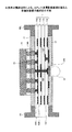
60 エアロゾルデポジション装置
61 処理容器
61A ステージ
61B ノズル
61a X−Yステージ駆動機構
61b Zステージ駆動機構
61c ジェット
62 メカニカルブースタポンプ
63 原料容器
63A 振動台
64 高圧ガス源
Claims (6)
- 各々配線パターンを担持し、さらに前記配線パターンに接続されたビアプラグを有する複数のビルドアップ樹脂層の積層よりなる樹脂積層体を備えたコアレス多層配線基板であって、
さらに前記樹脂積層体の上面および下面には、前記ビルドアップ層の弾性率よりも大きな弾性率を有する第1および第2のセラミック層が、それぞれ形成されており、
前記第1および第2のセラミック層の少なくとも一方は、金属パタ―ンに覆われて前記多層配線基板上において、前記多層配線基板に集積化されたキャパシタを形成することを特徴とするコアレス多層配線基板。 - 前記樹脂積層体の側壁面にもセラミック層が形成されていることを特徴とする請求項1記載のコアレス多層配線基板。
- 前記第1および第2のセラミック層は、エアロゾルデポジション法により形成されることを特徴とする請求項1または2記載のコアレス多層配線基板。
- 請求項1〜3のいずれか一項記載のコアレス多層配線基板と、前記多層配線基板上にフリップチップ実装された半導体チップよりなる半導体装置。
- 各々配線パターンを担持し、さらに前記配線パターンに接続されたビアプラグを有する複数のビルドアップ樹脂層の積層よりなる樹脂積層体を備えたコアレス多層配線基板の製造方法であって、
前記樹脂積層体の上面および下面には、前記ビルドアップ層の弾性率よりも大きな弾性率を有する第1および第2のセラミック層が、それぞれ形成されており、
前記第1および第2のセラミック層の少なくとも一方は、金属パタ―ンに覆われて前記多層配線基板上において、前記多層配線基板に集積化されたキャパシタを形成し、
前記第1および第2のセラミック層が、エアロゾルデポジション法により形成されることを特徴とするコアレス多層配線基板の製造方法。 - 前記樹脂積層体の側壁面にもセラミック層を形成する工程をさらに備えることを特徴とする請求項5記載のコアレス多層配線基板の製造方法。
Priority Applications (1)
| Application Number | Priority Date | Filing Date | Title |
|---|---|---|---|
| JP2006248641A JP5197942B2 (ja) | 2006-09-13 | 2006-09-13 | コアレス多層配線基板および半導体装置、その製造方法 |
Applications Claiming Priority (1)
| Application Number | Priority Date | Filing Date | Title |
|---|---|---|---|
| JP2006248641A JP5197942B2 (ja) | 2006-09-13 | 2006-09-13 | コアレス多層配線基板および半導体装置、その製造方法 |
Publications (2)
| Publication Number | Publication Date |
|---|---|
| JP2008071905A JP2008071905A (ja) | 2008-03-27 |
| JP5197942B2 true JP5197942B2 (ja) | 2013-05-15 |
Family
ID=39293249
Family Applications (1)
| Application Number | Title | Priority Date | Filing Date |
|---|---|---|---|
| JP2006248641A Expired - Fee Related JP5197942B2 (ja) | 2006-09-13 | 2006-09-13 | コアレス多層配線基板および半導体装置、その製造方法 |
Country Status (1)
| Country | Link |
|---|---|
| JP (1) | JP5197942B2 (ja) |
Families Citing this family (2)
| Publication number | Priority date | Publication date | Assignee | Title |
|---|---|---|---|---|
| JP2011146408A (ja) * | 2008-03-28 | 2011-07-28 | Nec Corp | 配線基板、半導体パッケージおよび配線基板の製造方法 |
| KR20190027579A (ko) * | 2017-09-07 | 2019-03-15 | 삼성전기주식회사 | 인쇄회로기판 |
Family Cites Families (5)
| Publication number | Priority date | Publication date | Assignee | Title |
|---|---|---|---|---|
| DE3207330A1 (de) * | 1982-03-02 | 1983-09-08 | Basf Ag, 6700 Ludwigshafen | Neue zubereitungen von phthalocyaninen und deren verwendung |
| JPH11145580A (ja) * | 1997-11-10 | 1999-05-28 | Daisho Denshi:Kk | プリント基板の製造方法 |
| JPH11251723A (ja) * | 1998-02-26 | 1999-09-17 | Kyocera Corp | 回路基板 |
| JP4427874B2 (ja) * | 2000-07-06 | 2010-03-10 | 住友ベークライト株式会社 | 多層配線板の製造方法および多層配線板 |
| JP4478401B2 (ja) * | 2003-05-15 | 2010-06-09 | 富士通株式会社 | 回路基板、電子装置、及び回路基板の製造方法 |
-
2006
- 2006-09-13 JP JP2006248641A patent/JP5197942B2/ja not_active Expired - Fee Related
Also Published As
| Publication number | Publication date |
|---|---|
| JP2008071905A (ja) | 2008-03-27 |
Similar Documents
| Publication | Publication Date | Title |
|---|---|---|
| JP4929784B2 (ja) | 多層配線基板、半導体装置およびソルダレジスト | |
| JP5258045B2 (ja) | 配線基板、配線基板を用いた半導体装置、及びそれらの製造方法 | |
| US8080875B2 (en) | Interconnection substrate and semiconductor device, manufacturing method of interconnection substrate | |
| WO2007126090A1 (ja) | 回路基板、電子デバイス装置及び回路基板の製造方法 | |
| JP2009141041A (ja) | 電子部品実装用パッケージ | |
| JP5367523B2 (ja) | 配線基板及び配線基板の製造方法 | |
| US20100108371A1 (en) | Wiring board with built-in electronic component and method for manufacturing the same | |
| US7619316B2 (en) | Semiconductor package and method for manufacturing the same | |
| JP5164403B2 (ja) | コアレス多層配線基板および半導体装置、その製造方法 | |
| JP4832369B2 (ja) | 回路基板、半導体装置、回路基板の製造方法、半導体装置の製造方法 | |
| US8581421B2 (en) | Semiconductor package manufacturing method and semiconductor package | |
| JP6151724B2 (ja) | 実装構造体の製造方法 | |
| JP2010129992A (ja) | 配線基板 | |
| JP6294024B2 (ja) | 配線基板およびこれを用いた実装構造体 | |
| JP4714510B2 (ja) | 配線基板の製造方法 | |
| JP5197942B2 (ja) | コアレス多層配線基板および半導体装置、その製造方法 | |
| JP6105316B2 (ja) | 電子装置 | |
| JP4445777B2 (ja) | 配線基板、及び配線基板の製造方法 | |
| JP4983288B2 (ja) | 多層配線基板およびその製造方法 | |
| JP5103948B2 (ja) | 電子部品および電子部品の製造方法 | |
| JP2009076928A (ja) | 配線基板の製造方法 | |
| JP2005353953A (ja) | 印刷配線板及び半導体装置 | |
| JP2004111544A (ja) | 多層配線基板 | |
| JP3834305B2 (ja) | 多層配線基板の製造方法 | |
| JP2006270079A (ja) | 配線基板及び配線基板の製造方法 |
Legal Events
| Date | Code | Title | Description |
|---|---|---|---|
| A621 | Written request for application examination |
Free format text: JAPANESE INTERMEDIATE CODE: A621 Effective date: 20090319 |
|
| A977 | Report on retrieval |
Free format text: JAPANESE INTERMEDIATE CODE: A971007 Effective date: 20110427 |
|
| A131 | Notification of reasons for refusal |
Free format text: JAPANESE INTERMEDIATE CODE: A131 Effective date: 20110510 |
|
| A521 | Request for written amendment filed |
Free format text: JAPANESE INTERMEDIATE CODE: A523 Effective date: 20110706 |
|
| A02 | Decision of refusal |
Free format text: JAPANESE INTERMEDIATE CODE: A02 Effective date: 20120214 |
|
| A61 | First payment of annual fees (during grant procedure) |
Free format text: JAPANESE INTERMEDIATE CODE: A61 Effective date: 20130206 |
|
| FPAY | Renewal fee payment (event date is renewal date of database) |
Free format text: PAYMENT UNTIL: 20160215 Year of fee payment: 3 |
|
| R150 | Certificate of patent or registration of utility model |
Free format text: JAPANESE INTERMEDIATE CODE: R150 Ref document number: 5197942 Country of ref document: JP Free format text: JAPANESE INTERMEDIATE CODE: R150 |
|
| LAPS | Cancellation because of no payment of annual fees |