JP5167267B2 - パッシブ・マトリックス式薄膜エレクトロルミネッセンス・ディスプレイ - Google Patents
パッシブ・マトリックス式薄膜エレクトロルミネッセンス・ディスプレイ Download PDFInfo
- Publication number
- JP5167267B2 JP5167267B2 JP2009536237A JP2009536237A JP5167267B2 JP 5167267 B2 JP5167267 B2 JP 5167267B2 JP 2009536237 A JP2009536237 A JP 2009536237A JP 2009536237 A JP2009536237 A JP 2009536237A JP 5167267 B2 JP5167267 B2 JP 5167267B2
- Authority
- JP
- Japan
- Prior art keywords
- display
- resolution component
- component signal
- signal
- substrate
- Prior art date
- Legal status (The legal status is an assumption and is not a legal conclusion. Google has not performed a legal analysis and makes no representation as to the accuracy of the status listed.)
- Active
Links
- 239000011159 matrix material Substances 0.000 title claims description 51
- 239000010409 thin film Substances 0.000 title claims description 21
- 239000000758 substrate Substances 0.000 claims description 42
- 238000005401 electroluminescence Methods 0.000 claims description 18
- 238000004020 luminiscence type Methods 0.000 claims 1
- 238000000034 method Methods 0.000 description 41
- 239000010410 layer Substances 0.000 description 27
- 238000010586 diagram Methods 0.000 description 12
- 239000000463 material Substances 0.000 description 12
- 230000002123 temporal effect Effects 0.000 description 5
- 230000008569 process Effects 0.000 description 3
- 230000004044 response Effects 0.000 description 3
- 230000000007 visual effect Effects 0.000 description 3
- 230000006870 function Effects 0.000 description 2
- 238000004519 manufacturing process Methods 0.000 description 2
- 238000000059 patterning Methods 0.000 description 2
- 238000012545 processing Methods 0.000 description 2
- 238000012935 Averaging Methods 0.000 description 1
- 230000008901 benefit Effects 0.000 description 1
- 239000003990 capacitor Substances 0.000 description 1
- 238000000576 coating method Methods 0.000 description 1
- 239000003086 colorant Substances 0.000 description 1
- 238000010276 construction Methods 0.000 description 1
- 238000007796 conventional method Methods 0.000 description 1
- 238000000354 decomposition reaction Methods 0.000 description 1
- 238000007599 discharging Methods 0.000 description 1
- 230000000694 effects Effects 0.000 description 1
- 238000001704 evaporation Methods 0.000 description 1
- 239000012212 insulator Substances 0.000 description 1
- 239000002184 metal Substances 0.000 description 1
- 238000012986 modification Methods 0.000 description 1
- 230000004048 modification Effects 0.000 description 1
- 239000012044 organic layer Substances 0.000 description 1
- 238000000206 photolithography Methods 0.000 description 1
- 229920000642 polymer Polymers 0.000 description 1
- 238000003672 processing method Methods 0.000 description 1
- 239000002096 quantum dot Substances 0.000 description 1
- 150000003384 small molecules Chemical class 0.000 description 1
Images


Classifications
-
- G—PHYSICS
- G09—EDUCATION; CRYPTOGRAPHY; DISPLAY; ADVERTISING; SEALS
- G09G—ARRANGEMENTS OR CIRCUITS FOR CONTROL OF INDICATING DEVICES USING STATIC MEANS TO PRESENT VARIABLE INFORMATION
- G09G3/00—Control arrangements or circuits, of interest only in connection with visual indicators other than cathode-ray tubes
- G09G3/20—Control arrangements or circuits, of interest only in connection with visual indicators other than cathode-ray tubes for presentation of an assembly of a number of characters, e.g. a page, by composing the assembly by combination of individual elements arranged in a matrix no fixed position being assigned to or needed to be assigned to the individual characters or partial characters
- G09G3/22—Control arrangements or circuits, of interest only in connection with visual indicators other than cathode-ray tubes for presentation of an assembly of a number of characters, e.g. a page, by composing the assembly by combination of individual elements arranged in a matrix no fixed position being assigned to or needed to be assigned to the individual characters or partial characters using controlled light sources
- G09G3/30—Control arrangements or circuits, of interest only in connection with visual indicators other than cathode-ray tubes for presentation of an assembly of a number of characters, e.g. a page, by composing the assembly by combination of individual elements arranged in a matrix no fixed position being assigned to or needed to be assigned to the individual characters or partial characters using controlled light sources using electroluminescent panels
-
- G—PHYSICS
- G09—EDUCATION; CRYPTOGRAPHY; DISPLAY; ADVERTISING; SEALS
- G09G—ARRANGEMENTS OR CIRCUITS FOR CONTROL OF INDICATING DEVICES USING STATIC MEANS TO PRESENT VARIABLE INFORMATION
- G09G3/00—Control arrangements or circuits, of interest only in connection with visual indicators other than cathode-ray tubes
- G09G3/20—Control arrangements or circuits, of interest only in connection with visual indicators other than cathode-ray tubes for presentation of an assembly of a number of characters, e.g. a page, by composing the assembly by combination of individual elements arranged in a matrix no fixed position being assigned to or needed to be assigned to the individual characters or partial characters
- G09G3/34—Control arrangements or circuits, of interest only in connection with visual indicators other than cathode-ray tubes for presentation of an assembly of a number of characters, e.g. a page, by composing the assembly by combination of individual elements arranged in a matrix no fixed position being assigned to or needed to be assigned to the individual characters or partial characters by control of light from an independent source
- G09G3/36—Control arrangements or circuits, of interest only in connection with visual indicators other than cathode-ray tubes for presentation of an assembly of a number of characters, e.g. a page, by composing the assembly by combination of individual elements arranged in a matrix no fixed position being assigned to or needed to be assigned to the individual characters or partial characters by control of light from an independent source using liquid crystals
- G09G3/3611—Control of matrices with row and column drivers
- G09G3/3622—Control of matrices with row and column drivers using a passive matrix
-
- H—ELECTRICITY
- H10—SEMICONDUCTOR DEVICES; ELECTRIC SOLID-STATE DEVICES NOT OTHERWISE PROVIDED FOR
- H10K—ORGANIC ELECTRIC SOLID-STATE DEVICES
- H10K59/00—Integrated devices, or assemblies of multiple devices, comprising at least one organic light-emitting element covered by group H10K50/00
- H10K59/10—OLED displays
- H10K59/17—Passive-matrix OLED displays
-
- G—PHYSICS
- G09—EDUCATION; CRYPTOGRAPHY; DISPLAY; ADVERTISING; SEALS
- G09G—ARRANGEMENTS OR CIRCUITS FOR CONTROL OF INDICATING DEVICES USING STATIC MEANS TO PRESENT VARIABLE INFORMATION
- G09G2300/00—Aspects of the constitution of display devices
- G09G2300/02—Composition of display devices
- G09G2300/023—Display panel composed of stacked panels
-
- G—PHYSICS
- G09—EDUCATION; CRYPTOGRAPHY; DISPLAY; ADVERTISING; SEALS
- G09G—ARRANGEMENTS OR CIRCUITS FOR CONTROL OF INDICATING DEVICES USING STATIC MEANS TO PRESENT VARIABLE INFORMATION
- G09G2300/00—Aspects of the constitution of display devices
- G09G2300/06—Passive matrix structure, i.e. with direct application of both column and row voltages to the light emitting or modulating elements, other than LCD or OLED
-
- G—PHYSICS
- G09—EDUCATION; CRYPTOGRAPHY; DISPLAY; ADVERTISING; SEALS
- G09G—ARRANGEMENTS OR CIRCUITS FOR CONTROL OF INDICATING DEVICES USING STATIC MEANS TO PRESENT VARIABLE INFORMATION
- G09G2310/00—Command of the display device
- G09G2310/02—Addressing, scanning or driving the display screen or processing steps related thereto
- G09G2310/0202—Addressing of scan or signal lines
- G09G2310/0205—Simultaneous scanning of several lines in flat panels
- G09G2310/021—Double addressing, i.e. scanning two or more lines, e.g. lines 2 and 3; 4 and 5, at a time in a first field, followed by scanning two or more lines in another combination, e.g. lines 1 and 2; 3 and 4, in a second field
-
- G—PHYSICS
- G09—EDUCATION; CRYPTOGRAPHY; DISPLAY; ADVERTISING; SEALS
- G09G—ARRANGEMENTS OR CIRCUITS FOR CONTROL OF INDICATING DEVICES USING STATIC MEANS TO PRESENT VARIABLE INFORMATION
- G09G2330/00—Aspects of power supply; Aspects of display protection and defect management
- G09G2330/02—Details of power systems and of start or stop of display operation
- G09G2330/021—Power management, e.g. power saving
-
- G—PHYSICS
- G09—EDUCATION; CRYPTOGRAPHY; DISPLAY; ADVERTISING; SEALS
- G09G—ARRANGEMENTS OR CIRCUITS FOR CONTROL OF INDICATING DEVICES USING STATIC MEANS TO PRESENT VARIABLE INFORMATION
- G09G2360/00—Aspects of the architecture of display systems
- G09G2360/12—Frame memory handling
- G09G2360/123—Frame memory handling using interleaving
Landscapes
- Engineering & Computer Science (AREA)
- Physics & Mathematics (AREA)
- Computer Hardware Design (AREA)
- General Physics & Mathematics (AREA)
- Theoretical Computer Science (AREA)
- Chemical & Material Sciences (AREA)
- Crystallography & Structural Chemistry (AREA)
- Electroluminescent Light Sources (AREA)
- Control Of Indicators Other Than Cathode Ray Tubes (AREA)
- Control Of El Displays (AREA)
Description
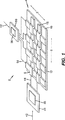
4 ディスプレイ
5、5a、5b エレクトロルミネッセンス素子
6 第1の方向
8 第2の方向
10 基板
11 柱
12 第1の電極
13 第1の電極
14 エレクトロルミネッセンス材料層
16 第2の電極
18 第2のエレクトロルミネッセンス材料層
19 第2の基板
20 第2の電極
24 第1の積層
26 第2の積層
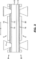
40 ドライバ
42 入力信号
44 駆動信号
46 回路
50 ドライバ
52 入力信号
54 駆動信号
56 回路
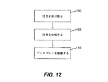
100 信号受信ステップ
105 信号分解ステップ
110 ディスプレイ駆動ステップ
Claims (5)
- a)i)第1の基板と、
ii)前記第1の基板の第1の方向に沿って複数のラインが形成されるようにパターニングされた第1の電極層と、
iii)前記第1の電極層の上に形成された1つ以上の第1の薄膜エレクトロルミネッセンス層と、
iv)1つ以上の前記第1の薄膜エレクトロルミネッセンス層の上に形成されていて、前記第1の基板の第1の方向とは異なる第2の方向に沿って複数のラインが形成されるようにパターニングされた第2の電極層と、を備えていて、
v)第1の電極層のラインと第2の電極層のラインの交点が、第1のエレクトロルミネッセンス・ユニットを含む個々の発光素子を規定しているディスプレイと、
b)i)前記ディスプレイの前記発光素子にアドレスするための入力画像信号を受け取り、
ii)前記入力画像信号を低解像度成分信号と高解像度成分信号に分解し、前記低解像度成分信号はアドレス可能な場所を前記高解像度成分信号の半数以下含んでいるようにし、
iii)前記ディスプレイを駆動するための駆動信号を供給することにより前記低解像度成分信号と前記高解像度成分信号を前記ディスプレイに独立に供給し、組み合わされた画像を形成する1つ以上のディスプレイ・ドライバと、を備え、
前記第1のエレクトロルミネッセンス・ユニットと重なるようにして配置された第2のエレクトロルミネッセンス・ユニットに含まれる1つ以上の第2の薄膜エレクトロルミネッセンス層、第3の電極層及び第4の電極層をさらに備え、
前記第1のエレクトロルミネッセンス・ユニットは前記低解像度成分信号を用いて第1のリフレッシュ・レートで駆動され、
前記第2のエレクトロルミネッセンス・ユニットは前記高解像度成分信号を用いて第2のリフレッシュ・レートで駆動される、
ことを特徴とするパッシブ・マトリックス式薄膜エレクトロルミネッセンス・ディスプレイ・システム。 - 前記低解像度成分信号が前記ディスプレイに供給されたときに、前記ディスプレイの2つの方向に沿った複数の発光素子がアクティブにされ、前記高解像度成分信号が前記ディスプレイに供給されたときに、前記ディスプレイの1つの方向だけに沿った複数の発光素子がアクティブにされる、請求項1に記載のパッシブ・マトリックス式薄膜エレクトロルミネッセンス・ディスプレイ・システム。
- 前記第1のエレクトロルミネッセンス・ユニット及び前記第2のエレクトロルミネッセンス・ユニットが前記第1の基板のいずれかの面に形成され、
前記第1の基板の第2の面には、前記第3の電極層、前記第2の薄膜エレクトロルミネッセンス層、及び前記第4の電極層が設けられている、請求項1に記載のパッシブ・マトリックス式薄膜エレクトロルミネッセンス・ディスプレイ・システム。 - 前記ディスプレイは第2の基板をさらに備え、
前記第1のエレクトロルミネッセンス・ユニットが、前記第1の基板の上で第1の積層の中に形成されていて前記低解像度成分信号によって駆動され、
前記第2のエレクトロルミネッセンス・ユニットが前記第2の基板の上で第2の積層の中に形成されていて前記高解像度成分信号によって駆動される、請求項1に記載のパッシブ・マトリックス式薄膜エレクトロルミネッセンス・ディスプレイ・システム。 - 前記第1及び第2のエレクトロルミネッセンス・ユニットを互いに積み重ね、前記第2の電極層及び前記第3の電極層を共通電極として共有する、請求項1に記載のパッシブ・マトリックス式薄膜エレクトロルミネッセンス・ディスプレイ・システム。
Applications Claiming Priority (3)
| Application Number | Priority Date | Filing Date | Title |
|---|---|---|---|
| US11/558,093 | 2006-11-09 | ||
| US11/558,093 US8049685B2 (en) | 2006-11-09 | 2006-11-09 | Passive matrix thin-film electro-luminescent display |
| PCT/US2007/022727 WO2008063348A2 (en) | 2006-11-09 | 2007-10-26 | Passive matrix thin-film electro-luminescent display |
Publications (3)
| Publication Number | Publication Date |
|---|---|
| JP2010509634A JP2010509634A (ja) | 2010-03-25 |
| JP2010509634A5 JP2010509634A5 (ja) | 2010-12-16 |
| JP5167267B2 true JP5167267B2 (ja) | 2013-03-21 |
Family
ID=39110882
Family Applications (1)
| Application Number | Title | Priority Date | Filing Date |
|---|---|---|---|
| JP2009536237A Active JP5167267B2 (ja) | 2006-11-09 | 2007-10-26 | パッシブ・マトリックス式薄膜エレクトロルミネッセンス・ディスプレイ |
Country Status (5)
| Country | Link |
|---|---|
| US (1) | US8049685B2 (ja) |
| EP (2) | EP2426659B1 (ja) |
| JP (1) | JP5167267B2 (ja) |
| KR (1) | KR101249459B1 (ja) |
| WO (1) | WO2008063348A2 (ja) |
Families Citing this family (11)
| Publication number | Priority date | Publication date | Assignee | Title |
|---|---|---|---|---|
| US8213519B2 (en) * | 2007-05-14 | 2012-07-03 | Sandisk Il, Ltd. | Methods of operating a dual decoder portable media device |
| DE102008024126A1 (de) * | 2008-05-19 | 2009-12-03 | X-Motive Gmbh | Verfahren und Treiber zum Ansteuern einer Passivmatrix-OLED-Anzeige |
| US8248358B2 (en) * | 2009-03-27 | 2012-08-21 | Qualcomm Mems Technologies, Inc. | Altering frame rates in a MEMS display by selective line skipping |
| US20130100176A1 (en) * | 2011-10-21 | 2013-04-25 | Qualcomm Mems Technologies, Inc. | Systems and methods for optimizing frame rate and resolution for displays |
| WO2013070947A1 (en) * | 2011-11-11 | 2013-05-16 | Qualcomm Mems Technologies, Inc. | Systems, devices, and methods for driving a plurality of display sections |
| CN103854596A (zh) * | 2012-11-29 | 2014-06-11 | 利亚德光电股份有限公司 | Led显示器 |
| US9524666B2 (en) | 2014-12-03 | 2016-12-20 | Revolution Display, Llc | OLED display modules for large-format OLED displays |
| US10417947B2 (en) * | 2015-06-30 | 2019-09-17 | Rockwell Collins, Inc. | Fail-operational emissive display with redundant drive elements |
| US9779478B1 (en) * | 2016-10-04 | 2017-10-03 | Oculus Vr, Llc | Rendering composite content on a head-mounted display including a high resolution inset |
| US10937924B2 (en) | 2016-10-08 | 2021-03-02 | Goertek. Inc | Display device and electronics apparatus |
| US10824022B2 (en) * | 2017-06-06 | 2020-11-03 | Liqxtal Technology Inc. | Liquid crystal lens and manufacturing method thereof |
Family Cites Families (86)
| Publication number | Priority date | Publication date | Assignee | Title |
|---|---|---|---|---|
| JPS5734286A (en) * | 1980-08-11 | 1982-02-24 | Canon Inc | Information outputting device |
| US4719385A (en) * | 1985-04-26 | 1988-01-12 | Barrow William A | Multi-colored thin-film electroluminescent display |
| GB8614876D0 (en) * | 1986-06-18 | 1986-07-23 | Rca Corp | Display processors |
| US4769292A (en) * | 1987-03-02 | 1988-09-06 | Eastman Kodak Company | Electroluminescent device with modified thin film luminescent zone |
| JPH01142694A (ja) * | 1987-11-04 | 1989-06-05 | Planar Syst Inc | 全色薄膜エレクトロルミネセンス表示装置 |
| US4886343A (en) * | 1988-06-20 | 1989-12-12 | Honeywell Inc. | Apparatus and method for additive/subtractive pixel arrangement in color mosaic displays |
| US5025394A (en) * | 1988-09-09 | 1991-06-18 | New York Institute Of Technology | Method and apparatus for generating animated images |
| US5061569A (en) * | 1990-07-26 | 1991-10-29 | Eastman Kodak Company | Electroluminescent device with organic electroluminescent medium |
| US5696531A (en) * | 1991-02-05 | 1997-12-09 | Minolta Camera Kabushiki Kaisha | Image display apparatus capable of combining image displayed with high resolution and image displayed with low resolution |
| JPH05181443A (ja) * | 1991-07-01 | 1993-07-23 | Seiko Epson Corp | コンピュータ |
| US5416494A (en) * | 1991-12-24 | 1995-05-16 | Nippondenso Co., Ltd. | Electroluminescent display |
| US5325449A (en) * | 1992-05-15 | 1994-06-28 | David Sarnoff Research Center, Inc. | Method for fusing images and apparatus therefor |
| JP3329887B2 (ja) * | 1992-06-17 | 2002-09-30 | ゼロックス・コーポレーション | 2光路液晶ライトバルブカラー表示装置 |
| JPH0638219A (ja) * | 1992-07-20 | 1994-02-10 | Olympus Optical Co Ltd | 映像表示装置 |
| US5488687A (en) * | 1992-09-17 | 1996-01-30 | Star Technologies, Inc. | Dual resolution output system for image generators |
| US5644324A (en) * | 1993-03-03 | 1997-07-01 | Maguire, Jr.; Francis J. | Apparatus and method for presenting successive images |
| US5808589A (en) * | 1994-08-24 | 1998-09-15 | Fergason; James L. | Optical system for a head mounted display combining high and low resolution images |
| US5703436A (en) * | 1994-12-13 | 1997-12-30 | The Trustees Of Princeton University | Transparent contacts for organic devices |
| JPH08234702A (ja) * | 1995-02-28 | 1996-09-13 | Sony Corp | 表示装置 |
| US6396507B1 (en) * | 1996-09-13 | 2002-05-28 | Nippon Steel Corporation | Data storage/access network system for zooming image and method of the storage/access |
| EP0941615B1 (en) * | 1997-09-30 | 2006-07-26 | Koninklijke Philips Electronics N.V. | Method for mixing pictures and a display apparatus |
| JP4081852B2 (ja) * | 1998-04-30 | 2008-04-30 | ソニー株式会社 | 有機el素子のマトリクス駆動方法及び有機el素子のマトリクス駆動装置 |
| JPH11338423A (ja) * | 1998-05-15 | 1999-12-10 | Internatl Business Mach Corp <Ibm> | カラー表示方法、この表示方法に適するマトリックス駆動用液晶表示モジュール、及び、この液晶表示モジュールを含むpcシステム、並びに、プロジェクションタイプ表示装置 |
| US6734838B1 (en) * | 1998-05-18 | 2004-05-11 | Dimension Technologies Inc. | Enhanced resolution for image generation |
| US6274980B1 (en) * | 1998-11-16 | 2001-08-14 | The Trustees Of Princeton University | Single-color stacked organic light emitting device |
| US6222675B1 (en) * | 1998-12-01 | 2001-04-24 | Kaiser Electro-Optics, Inc. | Area of interest head-mounted display using low resolution, wide angle; high resolution, narrow angle; and see-through views |
| US6078427A (en) * | 1998-12-01 | 2000-06-20 | Kaiser Electro-Optics, Inc. | Smooth transition device for area of interest head-mounted display |
| US6614448B1 (en) * | 1998-12-28 | 2003-09-02 | Nvidia Corporation | Circuit and method for displaying images using multisamples of non-uniform color resolution |
| US6819649B1 (en) * | 1999-02-12 | 2004-11-16 | D Data Inc. | Electroluminescent multilayer optical information storage medium with integrated readout and compositions of matter for use therein |
| JP3850625B2 (ja) * | 1999-04-02 | 2006-11-29 | 株式会社日立製作所 | 表示装置および表示方法 |
| US6781606B2 (en) * | 1999-05-20 | 2004-08-24 | Hewlett-Packard Development Company, L.P. | System and method for displaying images using foveal video |
| US6657603B1 (en) * | 1999-05-28 | 2003-12-02 | Lasergraphics, Inc. | Projector with circulating pixels driven by line-refresh-coordinated digital images |
| US6677948B1 (en) * | 1999-06-14 | 2004-01-13 | Mitutoyo Corporation | Systems and methods for multi-resolution image defocusing |
| GB2356757B (en) * | 1999-11-29 | 2004-02-04 | Seos Displays Ltd | Image display apparatus |
| KR100717199B1 (ko) * | 2000-02-01 | 2007-05-11 | 코닌클리케 필립스 일렉트로닉스 엔.브이. | 매트릭스 디스플레이 디바이스 상에 이미지를 디스플레이 하는 방법, 및 이러한 매트릭스 디스플레이 디바이스를 포함하는 디스플레이 장치 |
| US6873343B2 (en) * | 2000-05-11 | 2005-03-29 | Zoran Corporation | Scalable graphics image drawings on multiresolution image with/without image data re-usage |
| JP2001350453A (ja) * | 2000-06-08 | 2001-12-21 | Hitachi Ltd | 画像表示方法および画像表示装置 |
| US7110012B2 (en) * | 2000-06-12 | 2006-09-19 | Sharp Laboratories Of America, Inc. | System for improving display resolution |
| ATE343807T1 (de) * | 2000-08-08 | 2006-11-15 | Koninkl Philips Electronics Nv | Anzeigegerät |
| JP4633920B2 (ja) * | 2000-12-14 | 2011-02-16 | 株式会社日立製作所 | 表示装置および表示方法 |
| JP2002082647A (ja) * | 2000-09-05 | 2002-03-22 | Hitachi Ltd | 表示装置および表示方法 |
| US7027013B2 (en) * | 2000-12-22 | 2006-04-11 | Ifire Technology, Inc. | Shared pixel electroluminescent display driver system |
| JP3494146B2 (ja) * | 2000-12-28 | 2004-02-03 | 日本電気株式会社 | 有機el駆動回路及びパッシブマトリクス有機el表示装置並びに有機el駆動方法 |
| US6639706B2 (en) * | 2001-01-24 | 2003-10-28 | Kollsman, Inc. | Optical path switch and method of using thereof |
| JP2004523795A (ja) * | 2001-02-21 | 2004-08-05 | コーニンクレッカ フィリップス エレクトロニクス エヌ ヴィ | ビデオ信号を処理する表示システム |
| US7081870B2 (en) * | 2001-05-09 | 2006-07-25 | Hewlett-Packard Development Company, L.P. | Wearable display and method of displaying images using a wearable display |
| US7333071B2 (en) * | 2001-05-11 | 2008-02-19 | Xerox Corporation | Methods of using mixed resolution displays |
| US7546540B2 (en) * | 2001-05-11 | 2009-06-09 | Xerox Corporation | Methods of using mixed resolution displays |
| US7629945B2 (en) * | 2001-05-11 | 2009-12-08 | Xerox Corporation | Mixed resolution displays |
| US7475356B2 (en) * | 2001-05-11 | 2009-01-06 | Xerox Corporation | System utilizing mixed resolution displays |
| US6486607B1 (en) * | 2001-07-19 | 2002-11-26 | Jian-Jong Yeuan | Circuit and system for driving organic thin-film EL elements |
| JP4602608B2 (ja) * | 2001-08-28 | 2010-12-22 | 株式会社日立製作所 | 表示装置 |
| KR20030013933A (ko) * | 2001-08-10 | 2003-02-15 | 엘지.필립스 엘시디 주식회사 | 액정표시패널의 구동방법 |
| US7002533B2 (en) * | 2001-08-17 | 2006-02-21 | Michel Sayag | Dual-stage high-contrast electronic image display |
| KR100444498B1 (ko) * | 2001-09-21 | 2004-08-16 | 엘지전자 주식회사 | 하이브리드 일렉트로 루미네센스 패널 |
| JP2003230010A (ja) * | 2001-11-30 | 2003-08-15 | Ricoh Co Ltd | 画像処理装置及び画像処理方法 |
| US7123780B2 (en) * | 2001-12-11 | 2006-10-17 | Sony Corporation | Resolution enhancement for images stored in a database |
| US6936856B2 (en) * | 2002-01-15 | 2005-08-30 | Osram Opto Semiconductors Gmbh | Multi substrate organic light emitting devices |
| US6872472B2 (en) * | 2002-02-15 | 2005-03-29 | Eastman Kodak Company | Providing an organic electroluminescent device having stacked electroluminescent units |
| GB0209502D0 (en) * | 2002-04-25 | 2002-06-05 | Cambridge Display Tech Ltd | Display driver circuits |
| JP2004031214A (ja) * | 2002-06-27 | 2004-01-29 | Matsushita Electric Ind Co Ltd | 有機電界発光素子 |
| US6898331B2 (en) * | 2002-08-28 | 2005-05-24 | Bae Systems Aircraft Controls, Inc. | Image fusion system and method |
| KR100436715B1 (ko) * | 2002-11-04 | 2004-06-22 | 삼성에스디아이 주식회사 | 영상의 재현성을 증진시키기 위한 영상 데이터의 고속처리 방법 |
| JP4170068B2 (ja) * | 2002-11-12 | 2008-10-22 | シャープ株式会社 | データ信号線駆動方法、データ信号線駆動回路およびそれを用いた表示装置 |
| US7230594B2 (en) * | 2002-12-16 | 2007-06-12 | Eastman Kodak Company | Color OLED display with improved power efficiency |
| JP2004219759A (ja) * | 2003-01-15 | 2004-08-05 | Chi Mei Electronics Corp | 画像表示処理方法、画像表示処理装置、画像表示装置および画像表示処理システム |
| US20040145536A1 (en) * | 2003-01-29 | 2004-07-29 | Stephany Thomas M. | Hand-held device having a window and a flexible, retractable-detractable display for permitting an image to be viewed from either the window or the display |
| JP4402358B2 (ja) * | 2003-03-05 | 2010-01-20 | キヤノン株式会社 | カラー画像表示パネルおよびその駆動方法 |
| FR2854525B1 (fr) * | 2003-04-29 | 2005-06-17 | Canon Kk | Selection de la taille de decodage d'une image multi-resolutions. |
| US7495638B2 (en) * | 2003-05-13 | 2009-02-24 | Research Triangle Institute | Visual display with increased field of view |
| US6909233B2 (en) * | 2003-06-11 | 2005-06-21 | Eastman Kodak Company | Stacked OLED display having improved efficiency |
| JP4459576B2 (ja) * | 2003-08-29 | 2010-04-28 | オプトレックス株式会社 | 液晶表示装置 |
| US6980182B1 (en) * | 2003-10-22 | 2005-12-27 | Rockwell Collins | Display system |
| US20050116968A1 (en) * | 2003-12-02 | 2005-06-02 | John Barrus | Multi-capability display |
| US6850352B1 (en) * | 2004-01-08 | 2005-02-01 | Hewlett-Packard Development Company, L.P. | Method and system for generating color using a low-resolution spatial color modulator and a high-resolution modulator |
| US7528810B2 (en) * | 2004-05-25 | 2009-05-05 | Victor Company Of Japan, Limited | Display with multiple emission layers |
| JP4571437B2 (ja) * | 2004-05-31 | 2010-10-27 | インターナショナル・ビジネス・マシーンズ・コーポレーション | 解像度が異なる複数のウィンドウを表示するためのシステム、方法およびプログラム |
| JP3793214B2 (ja) * | 2004-08-30 | 2006-07-05 | キヤノン株式会社 | 表示装置及びその制御方法 |
| US7609230B2 (en) * | 2004-09-23 | 2009-10-27 | Hewlett-Packard Development Company, L.P. | Display method and system using transmissive and emissive components |
| GB0421712D0 (en) | 2004-09-30 | 2004-11-03 | Cambridge Display Tech Ltd | Multi-line addressing methods and apparatus |
| US7973747B2 (en) * | 2004-10-28 | 2011-07-05 | Panasonic Corporation | Display and display driving method |
| TWI386744B (zh) * | 2004-12-14 | 2013-02-21 | Samsung Display Co Ltd | 薄膜電晶體面板以及使用該薄膜電晶體面板之液晶顯示器 |
| US7142179B2 (en) * | 2005-03-23 | 2006-11-28 | Eastman Kodak Company | OLED display device |
| KR101106561B1 (ko) * | 2005-12-19 | 2012-01-19 | 엘지디스플레이 주식회사 | 액정표시장치의 구동회로 및 이를 포함하는 액정표시장치 |
| TWI297479B (en) * | 2006-06-13 | 2008-06-01 | Novatek Microelectronics Corp | Method for display image frame and display apparatus using the same |
| US7855752B2 (en) * | 2006-07-31 | 2010-12-21 | Hewlett-Packard Development Company, L.P. | Method and system for producing seamless composite images having non-uniform resolution from a multi-imager system |
-
2006
- 2006-11-09 US US11/558,093 patent/US8049685B2/en active Active
-
2007
- 2007-10-26 EP EP11008346.6A patent/EP2426659B1/en active Active
- 2007-10-26 KR KR1020097009411A patent/KR101249459B1/ko active IP Right Grant
- 2007-10-26 WO PCT/US2007/022727 patent/WO2008063348A2/en active Application Filing
- 2007-10-26 JP JP2009536237A patent/JP5167267B2/ja active Active
- 2007-10-26 EP EP07861540A patent/EP2092504A2/en not_active Ceased
Also Published As
| Publication number | Publication date |
|---|---|
| EP2092504A2 (en) | 2009-08-26 |
| KR20090086212A (ko) | 2009-08-11 |
| JP2010509634A (ja) | 2010-03-25 |
| EP2426659B1 (en) | 2013-12-11 |
| US8049685B2 (en) | 2011-11-01 |
| WO2008063348A2 (en) | 2008-05-29 |
| KR101249459B1 (ko) | 2013-03-29 |
| EP2426659A1 (en) | 2012-03-07 |
| WO2008063348A3 (en) | 2008-12-04 |
| US20080111771A1 (en) | 2008-05-15 |
Similar Documents
| Publication | Publication Date | Title |
|---|---|---|
| JP5167267B2 (ja) | パッシブ・マトリックス式薄膜エレクトロルミネッセンス・ディスプレイ | |
| US11568810B2 (en) | Display apparatus | |
| US7995002B2 (en) | Tiled passive matrix electro-luminescent display | |
| JP4909041B2 (ja) | 電界発光表示装置とその駆動方法 | |
| KR100685844B1 (ko) | 양면발광 유기 전계발광 표시장치 및 그의 구동방법 | |
| US6924602B2 (en) | Organic EL pixel circuit | |
| JP5616110B2 (ja) | 有機電界発光表示装置 | |
| KR100578841B1 (ko) | 발광 표시 장치와, 그 표시 패널 및 구동 방법 | |
| JP2010020208A (ja) | 走査駆動回路及び走査駆動回路を備えた表示装置 | |
| JP2006018297A (ja) | 逆多重化装置および逆多重化装置を用いる表示装置,逆多重化装置を用いる表示装置の表示パネルとその駆動方法 | |
| JP2019061777A (ja) | 有機el表示装置 | |
| CN111430433A (zh) | 显示面板及显示装置 | |
| WO2003054845A1 (en) | Active matrix electroluminescent display device | |
| JP4210244B2 (ja) | エレクトロルミネセンス表示装置 | |
| JP2007140276A (ja) | アクティブマトリクス型表示装置 | |
| KR20140080734A (ko) | 유기 발광 디스플레이 장치 | |
| KR101365779B1 (ko) | 유기발광다이오드 표시장치 | |
| JP2007065614A (ja) | エレクトロルミネセンス表示装置及びその駆動方法並びにエレクトロルミネセンス表示パネル | |
| JP2005352147A (ja) | アクティブマトリクス型発光表示パネル | |
| JP3981140B2 (ja) | 画像表示装置 | |
| KR100590064B1 (ko) | 발광표시 장치 및 그 구동 방법 | |
| KR20060091651A (ko) | 유기발광소자 | |
| JP3690643B2 (ja) | パッシブマトリクス有機薄膜発光ディスプレイ | |
| KR20070028752A (ko) | 전계 발광 표시장치와 그 구동방법 | |
| JP2007108503A (ja) | アクティブマトリックス型表示装置およびその駆動方法 |
Legal Events
| Date | Code | Title | Description |
|---|---|---|---|
| A711 | Notification of change in applicant |
Free format text: JAPANESE INTERMEDIATE CODE: A711 Effective date: 20100806 |
|
| A521 | Request for written amendment filed |
Free format text: JAPANESE INTERMEDIATE CODE: A523 Effective date: 20101026 |
|
| A621 | Written request for application examination |
Free format text: JAPANESE INTERMEDIATE CODE: A621 Effective date: 20101026 |
|
| A131 | Notification of reasons for refusal |
Free format text: JAPANESE INTERMEDIATE CODE: A131 Effective date: 20120626 |
|
| A521 | Request for written amendment filed |
Free format text: JAPANESE INTERMEDIATE CODE: A523 Effective date: 20120926 |
|
| TRDD | Decision of grant or rejection written | ||
| A01 | Written decision to grant a patent or to grant a registration (utility model) |
Free format text: JAPANESE INTERMEDIATE CODE: A01 Effective date: 20121127 |
|
| A61 | First payment of annual fees (during grant procedure) |
Free format text: JAPANESE INTERMEDIATE CODE: A61 Effective date: 20121221 |
|
| FPAY | Renewal fee payment (event date is renewal date of database) |
Free format text: PAYMENT UNTIL: 20151228 Year of fee payment: 3 |
|
| R150 | Certificate of patent or registration of utility model |
Ref document number: 5167267 Country of ref document: JP Free format text: JAPANESE INTERMEDIATE CODE: R150 Free format text: JAPANESE INTERMEDIATE CODE: R150 |
|
| R250 | Receipt of annual fees |
Free format text: JAPANESE INTERMEDIATE CODE: R250 |
|
| R250 | Receipt of annual fees |
Free format text: JAPANESE INTERMEDIATE CODE: R250 |
|
| R250 | Receipt of annual fees |
Free format text: JAPANESE INTERMEDIATE CODE: R250 |
|
| R250 | Receipt of annual fees |
Free format text: JAPANESE INTERMEDIATE CODE: R250 |
|
| R250 | Receipt of annual fees |
Free format text: JAPANESE INTERMEDIATE CODE: R250 |
|
| R250 | Receipt of annual fees |
Free format text: JAPANESE INTERMEDIATE CODE: R250 |
|
| R250 | Receipt of annual fees |
Free format text: JAPANESE INTERMEDIATE CODE: R250 |
|
| R250 | Receipt of annual fees |
Free format text: JAPANESE INTERMEDIATE CODE: R250 |
|
| R250 | Receipt of annual fees |
Free format text: JAPANESE INTERMEDIATE CODE: R250 |