JP5156235B2 - Fabrication method for nitride-based transistors - Google Patents
Fabrication method for nitride-based transistors Download PDFInfo
- Publication number
- JP5156235B2 JP5156235B2 JP2006549235A JP2006549235A JP5156235B2 JP 5156235 B2 JP5156235 B2 JP 5156235B2 JP 2006549235 A JP2006549235 A JP 2006549235A JP 2006549235 A JP2006549235 A JP 2006549235A JP 5156235 B2 JP5156235 B2 JP 5156235B2
- Authority
- JP
- Japan
- Prior art keywords
- layer
- nitride
- forming
- protective layer
- barrier layer
- Prior art date
- Legal status (The legal status is an assumption and is not a legal conclusion. Google has not performed a legal analysis and makes no representation as to the accuracy of the status listed.)
- Active
Links
- 238000000034 method Methods 0.000 title claims description 56
- 150000004767 nitrides Chemical class 0.000 title claims description 55
- 238000004519 manufacturing process Methods 0.000 title description 21
- 239000010410 layer Substances 0.000 claims description 275
- 239000011241 protective layer Substances 0.000 claims description 134
- 230000004888 barrier function Effects 0.000 claims description 106
- 238000002161 passivation Methods 0.000 claims description 42
- 229910002601 GaN Inorganic materials 0.000 claims description 39
- JMASRVWKEDWRBT-UHFFFAOYSA-N Gallium nitride Chemical compound [Ga]#N JMASRVWKEDWRBT-UHFFFAOYSA-N 0.000 claims description 33
- 239000000463 material Substances 0.000 claims description 32
- 229910052751 metal Inorganic materials 0.000 claims description 26
- 239000002184 metal Substances 0.000 claims description 26
- 239000004065 semiconductor Substances 0.000 claims description 25
- 239000000758 substrate Substances 0.000 claims description 25
- 238000005530 etching Methods 0.000 claims description 24
- PMHQVHHXPFUNSP-UHFFFAOYSA-M copper(1+);methylsulfanylmethane;bromide Chemical compound Br[Cu].CSC PMHQVHHXPFUNSP-UHFFFAOYSA-M 0.000 claims description 23
- 229910052581 Si3N4 Inorganic materials 0.000 claims description 12
- 229910004298 SiO 2 Inorganic materials 0.000 claims description 12
- 238000000137 annealing Methods 0.000 claims description 12
- HQVNEWCFYHHQES-UHFFFAOYSA-N silicon nitride Chemical compound N12[Si]34N5[Si]62N3[Si]51N64 HQVNEWCFYHHQES-UHFFFAOYSA-N 0.000 claims description 12
- RNQKDQAVIXDKAG-UHFFFAOYSA-N aluminum gallium Chemical compound [Al].[Ga] RNQKDQAVIXDKAG-UHFFFAOYSA-N 0.000 claims description 9
- VYPSYNLAJGMNEJ-UHFFFAOYSA-N Silicium dioxide Chemical compound O=[Si]=O VYPSYNLAJGMNEJ-UHFFFAOYSA-N 0.000 claims description 8
- AJGDITRVXRPLBY-UHFFFAOYSA-N aluminum indium Chemical compound [Al].[In] AJGDITRVXRPLBY-UHFFFAOYSA-N 0.000 claims description 7
- 239000000203 mixture Substances 0.000 claims description 7
- 238000000151 deposition Methods 0.000 claims description 6
- PIGFYZPCRLYGLF-UHFFFAOYSA-N Aluminum nitride Chemical compound [Al]#N PIGFYZPCRLYGLF-UHFFFAOYSA-N 0.000 claims description 4
- 229910052738 indium Inorganic materials 0.000 claims description 4
- APFVFJFRJDLVQX-UHFFFAOYSA-N indium atom Chemical compound [In] APFVFJFRJDLVQX-UHFFFAOYSA-N 0.000 claims description 4
- 235000012239 silicon dioxide Nutrition 0.000 claims description 4
- 239000000377 silicon dioxide Substances 0.000 claims description 4
- 238000002488 metal-organic chemical vapour deposition Methods 0.000 claims description 3
- 238000011065 in-situ storage Methods 0.000 claims description 2
- 238000001039 wet etching Methods 0.000 claims description 2
- -1 AlGaN Chemical compound 0.000 claims 1
- HBMJWWWQQXIZIP-UHFFFAOYSA-N silicon carbide Chemical compound [Si+]#[C-] HBMJWWWQQXIZIP-UHFFFAOYSA-N 0.000 description 15
- 230000015572 biosynthetic process Effects 0.000 description 14
- 229910010271 silicon carbide Inorganic materials 0.000 description 14
- 238000010586 diagram Methods 0.000 description 11
- IJGRMHOSHXDMSA-UHFFFAOYSA-N Atomic nitrogen Chemical compound N#N IJGRMHOSHXDMSA-UHFFFAOYSA-N 0.000 description 6
- 150000001875 compounds Chemical class 0.000 description 6
- 230000007704 transition Effects 0.000 description 6
- JBRZTFJDHDCESZ-UHFFFAOYSA-N AsGa Chemical compound [As]#[Ga] JBRZTFJDHDCESZ-UHFFFAOYSA-N 0.000 description 5
- 229910052782 aluminium Inorganic materials 0.000 description 5
- XAGFODPZIPBFFR-UHFFFAOYSA-N aluminium Chemical compound [Al] XAGFODPZIPBFFR-UHFFFAOYSA-N 0.000 description 5
- 238000005229 chemical vapour deposition Methods 0.000 description 5
- 229920002120 photoresistant polymer Polymers 0.000 description 5
- 238000005240 physical vapour deposition Methods 0.000 description 5
- 239000002356 single layer Substances 0.000 description 5
- 229910001218 Gallium arsenide Inorganic materials 0.000 description 4
- 230000008901 benefit Effects 0.000 description 4
- 238000001020 plasma etching Methods 0.000 description 4
- XUIMIQQOPSSXEZ-UHFFFAOYSA-N Silicon Chemical compound [Si] XUIMIQQOPSSXEZ-UHFFFAOYSA-N 0.000 description 3
- 230000015556 catabolic process Effects 0.000 description 3
- 239000013078 crystal Substances 0.000 description 3
- 238000009616 inductively coupled plasma Methods 0.000 description 3
- CPLXHLVBOLITMK-UHFFFAOYSA-N magnesium oxide Inorganic materials [Mg]=O CPLXHLVBOLITMK-UHFFFAOYSA-N 0.000 description 3
- 229910052757 nitrogen Inorganic materials 0.000 description 3
- 230000006911 nucleation Effects 0.000 description 3
- 238000010899 nucleation Methods 0.000 description 3
- 229910052594 sapphire Inorganic materials 0.000 description 3
- 239000010980 sapphire Substances 0.000 description 3
- 229910052710 silicon Inorganic materials 0.000 description 3
- 239000010703 silicon Substances 0.000 description 3
- 238000004544 sputter deposition Methods 0.000 description 3
- KRHYYFGTRYWZRS-UHFFFAOYSA-N Fluorane Chemical compound F KRHYYFGTRYWZRS-UHFFFAOYSA-N 0.000 description 2
- 230000008021 deposition Effects 0.000 description 2
- 230000000694 effects Effects 0.000 description 2
- 230000005669 field effect Effects 0.000 description 2
- 239000012535 impurity Substances 0.000 description 2
- 239000000395 magnesium oxide Substances 0.000 description 2
- TWNQGVIAIRXVLR-UHFFFAOYSA-N oxo(oxoalumanyloxy)alumane Chemical compound O=[Al]O[Al]=O TWNQGVIAIRXVLR-UHFFFAOYSA-N 0.000 description 2
- 230000010287 polarization Effects 0.000 description 2
- 230000001681 protective effect Effects 0.000 description 2
- GYHNNYVSQQEPJS-UHFFFAOYSA-N Gallium Chemical compound [Ga] GYHNNYVSQQEPJS-UHFFFAOYSA-N 0.000 description 1
- 229910005883 NiSi Inorganic materials 0.000 description 1
- 229910004205 SiNX Inorganic materials 0.000 description 1
- 229910008807 WSiN Inorganic materials 0.000 description 1
- 238000009825 accumulation Methods 0.000 description 1
- 230000002411 adverse Effects 0.000 description 1
- 229910045601 alloy Inorganic materials 0.000 description 1
- 239000000956 alloy Substances 0.000 description 1
- 229910021431 alpha silicon carbide Inorganic materials 0.000 description 1
- 239000000969 carrier Substances 0.000 description 1
- 229910052804 chromium Inorganic materials 0.000 description 1
- 239000011248 coating agent Substances 0.000 description 1
- 238000000576 coating method Methods 0.000 description 1
- 229910052802 copper Inorganic materials 0.000 description 1
- 230000007547 defect Effects 0.000 description 1
- 230000006866 deterioration Effects 0.000 description 1
- 239000002019 doping agent Substances 0.000 description 1
- 229910052733 gallium Inorganic materials 0.000 description 1
- 230000017525 heat dissipation Effects 0.000 description 1
- 238000010438 heat treatment Methods 0.000 description 1
- 238000002248 hydride vapour-phase epitaxy Methods 0.000 description 1
- 238000002955 isolation Methods 0.000 description 1
- AXZKOIWUVFPNLO-UHFFFAOYSA-N magnesium;oxygen(2-) Chemical compound [O-2].[Mg+2] AXZKOIWUVFPNLO-UHFFFAOYSA-N 0.000 description 1
- 238000001465 metallisation Methods 0.000 description 1
- 229910052759 nickel Inorganic materials 0.000 description 1
- 229910052763 palladium Inorganic materials 0.000 description 1
- 230000003071 parasitic effect Effects 0.000 description 1
- 238000000059 patterning Methods 0.000 description 1
- 230000000737 periodic effect Effects 0.000 description 1
- 238000000206 photolithography Methods 0.000 description 1
- 238000000623 plasma-assisted chemical vapour deposition Methods 0.000 description 1
- 229910052697 platinum Inorganic materials 0.000 description 1
- HYXGAEYDKFCVMU-UHFFFAOYSA-N scandium oxide Chemical compound O=[Sc]O[Sc]=O HYXGAEYDKFCVMU-UHFFFAOYSA-N 0.000 description 1
- 230000035945 sensitivity Effects 0.000 description 1
- 229910052721 tungsten Inorganic materials 0.000 description 1
- 230000005533 two-dimensional electron gas Effects 0.000 description 1
Images


Classifications
-
- H—ELECTRICITY
- H01—ELECTRIC ELEMENTS
- H01L—SEMICONDUCTOR DEVICES NOT COVERED BY CLASS H10
- H01L29/00—Semiconductor devices adapted for rectifying, amplifying, oscillating or switching, or capacitors or resistors with at least one potential-jump barrier or surface barrier, e.g. PN junction depletion layer or carrier concentration layer; Details of semiconductor bodies or of electrodes thereof ; Multistep manufacturing processes therefor
- H01L29/66—Types of semiconductor device ; Multistep manufacturing processes therefor
- H01L29/68—Types of semiconductor device ; Multistep manufacturing processes therefor controllable by only the electric current supplied, or only the electric potential applied, to an electrode which does not carry the current to be rectified, amplified or switched
- H01L29/76—Unipolar devices, e.g. field effect transistors
- H01L29/772—Field effect transistors
- H01L29/778—Field effect transistors with two-dimensional charge carrier gas channel, e.g. HEMT ; with two-dimensional charge-carrier layer formed at a heterojunction interface
-
- H—ELECTRICITY
- H01—ELECTRIC ELEMENTS
- H01L—SEMICONDUCTOR DEVICES NOT COVERED BY CLASS H10
- H01L29/00—Semiconductor devices adapted for rectifying, amplifying, oscillating or switching, or capacitors or resistors with at least one potential-jump barrier or surface barrier, e.g. PN junction depletion layer or carrier concentration layer; Details of semiconductor bodies or of electrodes thereof ; Multistep manufacturing processes therefor
- H01L29/66—Types of semiconductor device ; Multistep manufacturing processes therefor
- H01L29/66007—Multistep manufacturing processes
- H01L29/66075—Multistep manufacturing processes of devices having semiconductor bodies comprising group 14 or group 13/15 materials
- H01L29/66227—Multistep manufacturing processes of devices having semiconductor bodies comprising group 14 or group 13/15 materials the devices being controllable only by the electric current supplied or the electric potential applied, to an electrode which does not carry the current to be rectified, amplified or switched, e.g. three-terminal devices
- H01L29/66409—Unipolar field-effect transistors
- H01L29/66446—Unipolar field-effect transistors with an active layer made of a group 13/15 material, e.g. group 13/15 velocity modulation transistor [VMT], group 13/15 negative resistance FET [NERFET]
- H01L29/66462—Unipolar field-effect transistors with an active layer made of a group 13/15 material, e.g. group 13/15 velocity modulation transistor [VMT], group 13/15 negative resistance FET [NERFET] with a heterojunction interface channel or gate, e.g. HFET, HIGFET, SISFET, HJFET, HEMT
-
- H—ELECTRICITY
- H01—ELECTRIC ELEMENTS
- H01L—SEMICONDUCTOR DEVICES NOT COVERED BY CLASS H10
- H01L21/00—Processes or apparatus adapted for the manufacture or treatment of semiconductor or solid state devices or of parts thereof
- H01L21/02—Manufacture or treatment of semiconductor devices or of parts thereof
- H01L21/04—Manufacture or treatment of semiconductor devices or of parts thereof the devices having at least one potential-jump barrier or surface barrier, e.g. PN junction, depletion layer or carrier concentration layer
- H01L21/18—Manufacture or treatment of semiconductor devices or of parts thereof the devices having at least one potential-jump barrier or surface barrier, e.g. PN junction, depletion layer or carrier concentration layer the devices having semiconductor bodies comprising elements of Group IV of the Periodic System or AIIIBV compounds with or without impurities, e.g. doping materials
-
- H—ELECTRICITY
- H01—ELECTRIC ELEMENTS
- H01L—SEMICONDUCTOR DEVICES NOT COVERED BY CLASS H10
- H01L29/00—Semiconductor devices adapted for rectifying, amplifying, oscillating or switching, or capacitors or resistors with at least one potential-jump barrier or surface barrier, e.g. PN junction depletion layer or carrier concentration layer; Details of semiconductor bodies or of electrodes thereof ; Multistep manufacturing processes therefor
- H01L29/66—Types of semiconductor device ; Multistep manufacturing processes therefor
- H01L29/68—Types of semiconductor device ; Multistep manufacturing processes therefor controllable by only the electric current supplied, or only the electric potential applied, to an electrode which does not carry the current to be rectified, amplified or switched
- H01L29/76—Unipolar devices, e.g. field effect transistors
- H01L29/772—Field effect transistors
- H01L29/778—Field effect transistors with two-dimensional charge carrier gas channel, e.g. HEMT ; with two-dimensional charge-carrier layer formed at a heterojunction interface
- H01L29/7782—Field effect transistors with two-dimensional charge carrier gas channel, e.g. HEMT ; with two-dimensional charge-carrier layer formed at a heterojunction interface with confinement of carriers by at least two heterojunctions, e.g. DHHEMT, quantum well HEMT, DHMODFET
- H01L29/7783—Field effect transistors with two-dimensional charge carrier gas channel, e.g. HEMT ; with two-dimensional charge-carrier layer formed at a heterojunction interface with confinement of carriers by at least two heterojunctions, e.g. DHHEMT, quantum well HEMT, DHMODFET using III-V semiconductor material
-
- H—ELECTRICITY
- H01—ELECTRIC ELEMENTS
- H01L—SEMICONDUCTOR DEVICES NOT COVERED BY CLASS H10
- H01L29/00—Semiconductor devices adapted for rectifying, amplifying, oscillating or switching, or capacitors or resistors with at least one potential-jump barrier or surface barrier, e.g. PN junction depletion layer or carrier concentration layer; Details of semiconductor bodies or of electrodes thereof ; Multistep manufacturing processes therefor
- H01L29/02—Semiconductor bodies ; Multistep manufacturing processes therefor
- H01L29/12—Semiconductor bodies ; Multistep manufacturing processes therefor characterised by the materials of which they are formed
- H01L29/20—Semiconductor bodies ; Multistep manufacturing processes therefor characterised by the materials of which they are formed including, apart from doping materials or other impurities, only AIIIBV compounds
- H01L29/2003—Nitride compounds
Description
本発明は半導体デバイスに関し、より詳細には、窒化物ベースの活性層を組み込んだトランジスタに関する。 The present invention relates to semiconductor devices, and more particularly to transistors incorporating nitride-based active layers.
シリコン(Si)やガリウムヒ素(GaAs)などの材料は、より低電力および(Siの場合には)より低周波用途向けの半導体デバイスに幅広く応用されてきている。しかし、よく知られているように、これらの半導体材料は、比較的小さなバンドギャップ(例えば、室温で、Siの場合には1.12eV、GaAsの場合には1.42eV)および/または比較的小さな破壊電圧のため、より高電力および/またはより高周波用途向けには適していない。 Materials such as silicon (Si) and gallium arsenide (GaAs) have been widely applied in semiconductor devices for lower power and (in the case of Si) lower frequency applications. However, as is well known, these semiconductor materials have a relatively small bandgap (eg, at room temperature, 1.12 eV for Si, 1.42 eV for GaAs) and / or relatively Due to the small breakdown voltage, it is not suitable for higher power and / or higher frequency applications.
SiおよびGaAsが示す難点に照らして、高電力、高温および/または高周波の用途ならびにデバイスにおける関心は、炭化ケイ素(α−SiCの場合には、室温で2.996eV)やIII族窒化物(例えば、GaNの場合には、室温で3.36eV)などの広バンドギャップの半導体材料に移ってきた。これらの材料は一般に、ガリウムヒ素およびシリコンと比べて、より高い電界破壊強度およびより高い電子飽和速度を有する。 In light of the difficulties presented by Si and GaAs, interest in high power, high temperature and / or high frequency applications and devices is of interest for silicon carbide (2.996 eV at room temperature for α-SiC) and III-nitrides (eg, In the case of GaN, it has moved to a wide band gap semiconductor material such as 3.36 eV at room temperature. These materials generally have higher field breakdown strengths and higher electron saturation rates compared to gallium arsenide and silicon.
高電力および/または高周波用途向けの、特に関心が寄せられているデバイスは、高電子移動度トランジスタ(HEMT)であり、これは変調ドープ電界効果トランジスタ(MODFET)としても知られる。これらのデバイスでは、異なるバンドギャップエネルギーを有し、かつバンドギャップが小さい方の材料がより高い電子親和力を有する2種類の半導体材料のヘテロ接合部で、2次元電子ガス(2DEG)が形成されるので、いくつかの状況のもとで、動作上の利点をもたらすことができる。2DEGは、非ドープの(「意図的でなくドープされた」)、バンドギャップが小さい方の材料中の蓄積層であり、例えば1013キャリア/cm2を上回る、非常に高いシート電子濃度を有することができる。さらに、バンドギャップが広い方の半導体中からの電子が2DEGに移動し、そこではイオン化不純物散乱が低減されているため、高い電子移動度を持つことが可能になる。 A device of particular interest for high power and / or high frequency applications is the high electron mobility transistor (HEMT), also known as a modulation doped field effect transistor (MODFET). In these devices, a two-dimensional electron gas (2DEG) is formed at a heterojunction of two semiconductor materials having different bandgap energies and the smaller bandgap material having a higher electron affinity. So it can bring operational advantages under some circumstances. 2DEG is an accumulation layer in an undoped (“unintentionally doped”), lower bandgap material, having a very high sheet electron concentration, eg, greater than 10 13 carriers / cm 2 be able to. Furthermore, electrons from the semiconductor with the wider band gap move to 2DEG, where ionized impurity scattering is reduced, so that high electron mobility can be achieved.
高キャリア濃度と高キャリア移動度がこのように組み合わさることにより、非常に大きな相互コンダクタンスをHEMTに与えることができ、また高周波用途向けの金属半導体電界効果トランジスタ(MESFET)に勝る、大きな性能上の利点をもたらすことができる。 This combination of high carrier concentration and high carrier mobility can provide very high transconductance to the HEMT and offers significant performance advantages over metal semiconductor field effect transistors (MESFETs) for high frequency applications. Can bring benefits.
窒化ガリウム/窒化アルミニウムガリウム(GaN/AlGaN)材料系で製作される高電子移動度トランジスタは、前述の高破壊電界、それらの材料の広いバンドギャップ、大きな伝導帯オフセット、および/または高飽和電子ドリフト速度を含めた材料特性を併せもつため、大きな高周波電力を発生する可能性を有する。2DEG中の電子の大部分は、AlGaN中の分極によるものとされている。GaN/AlGaN系によるHEMTは、これまでに示されている。AlGaN/GaN HEMT構造および製造方法は、文献に記載されている(特許文献1、特許文献2参照)。半絶縁性炭化ケイ素基板、基板上に窒化アルミニウムバッファ層、バッファ層上に絶縁性窒化ガリウム層、窒化ガリウム層上に窒化アルミニウムガリウムバリア層、窒化アルミニウムガリウムの活性構造上にパッシベーション層を有するHEMTデバイスが、文献に記載されている(特許文献3参照)。 High electron mobility transistors fabricated in the gallium nitride / aluminum gallium nitride (GaN / AlGaN) material system have the aforementioned high breakdown field, wide band gap of those materials, large conduction band offset, and / or high saturation electron drift. Since it has material characteristics including speed, it has the possibility of generating large high frequency power. Most of the electrons in 2DEG are attributed to polarization in AlGaN. GaN / AlGaN-based HEMTs have been shown so far. The AlGaN / GaN HEMT structure and manufacturing method are described in the literature (see Patent Document 1 and Patent Document 2). HEMT device having a semi-insulating silicon carbide substrate, an aluminum nitride buffer layer on the substrate, an insulating gallium nitride layer on the buffer layer, an aluminum gallium nitride barrier layer on the gallium nitride layer, and a passivation layer on the active structure of aluminum gallium nitride Is described in the literature (see Patent Document 3).
窒化物ベースのトランジスタの製作における1つの段階は、そうしたトランジスタ用のオーム性接触の形成である。オーム性接触の形成には一般に、高アニール温度(例えば900℃)が必要とされてきた。そうした高アニール温度は、材料および/またはデバイスに損傷を与えることがある。 One step in the fabrication of nitride-based transistors is the formation of ohmic contacts for such transistors. In general, high annealing temperatures (eg, 900 ° C.) have been required to form ohmic contacts. Such high annealing temperatures can damage materials and / or devices.
例えば、オーム性接触を形成する際に高アニール温度を利用する従来型のデバイスでは、AlGaN層および/またはGaN層のゲート領域(2つの接点間の活性デバイス領域と定義される)のシート抵抗は一般に、成長させたままのAlGaN層および/またはGaN層のシート抵抗に比べて増大する。シート抵抗のそうした増大は、デバイスに悪影響を及ぼすと考えられている。 For example, in conventional devices that utilize high annealing temperatures in forming ohmic contacts, the sheet resistance of the AlGaN layer and / or the gate region of the GaN layer (defined as the active device region between the two contacts) is Generally, it increases compared to the sheet resistance of the as-grown AlGaN layer and / or GaN layer. Such an increase in sheet resistance is believed to adversely affect the device.
本発明の諸実施形態は、窒化物ベースの半導体チャネル層上に窒化物ベースの半導体バリア層を形成し、窒化物ベースの半導体バリア層のゲート領域上に保護層を形成することによる、トランジスタの製作を提供する。バリア層上に、パターニングされたオーム性接触金属領域を形成し、それをアニールして、第1および第2のオーム性接触を形成する。アニールは、ゲート領域上に保護層を載せたままで実施される。ゲート接点も、バリア層のゲート領域(例えば、第1と第2のオーム性接触間の活性デバイス領域)上に形成される。 Embodiments of the present invention provide a transistor by forming a nitride-based semiconductor barrier layer on a nitride-based semiconductor channel layer and forming a protective layer on the gate region of the nitride-based semiconductor barrier layer. Provide production. A patterned ohmic contact metal region is formed on the barrier layer and annealed to form first and second ohmic contacts. The annealing is performed with the protective layer placed on the gate region. A gate contact is also formed on the gate region of the barrier layer (eg, the active device region between the first and second ohmic contacts).
本発明の別の諸実施形態では、パターニングされたオーム性接触金属をアニールした後に、保護層が除去される。保護層は窒化アルミニウム層でよい。保護層は、低損傷エッチング技術を利用して除去することができる。例えば、低損傷エッチング技術には、KOHなどの強塩基を用いた湿式除去が含まれ得る。保護層を除去した後に、バリア層の露出部分上に、パッシベーション層を形成することができる。これらの実施形態では、バリア層のゲート領域の一部分を露出させるために、低損傷エッチング技術を利用してパッシベーション層に陥凹部をエッチングし、パッシベーション層の陥凹部中にゲート接点を形成することによって、ゲート接点を形成することができる。 In other embodiments of the invention, the protective layer is removed after annealing the patterned ohmic contact metal. The protective layer may be an aluminum nitride layer. The protective layer can be removed using low damage etching techniques. For example, low damage etching techniques can include wet removal using a strong base such as KOH. After removing the protective layer, a passivation layer can be formed on the exposed portion of the barrier layer. In these embodiments, a low damage etch technique is used to etch a recess in the passivation layer to expose a portion of the gate region of the barrier layer, thereby forming a gate contact in the recess of the passivation layer. A gate contact can be formed.
本発明の別の諸実施形態では、バリア層および保護層の露出部分上に、パッシベーション層が形成される。これらの諸実施形態では、パッシベーション層および保護層を貫通して延びてバリア層に接触するゲート接点を形成することによって、ゲート接点を設けることができる。 In other embodiments of the present invention, a passivation layer is formed on the exposed portions of the barrier layer and the protective layer. In these embodiments, the gate contact can be provided by forming a gate contact that extends through the passivation layer and the protective layer to contact the barrier layer.
本発明の別の諸実施形態では、保護層を形成することは、バリア層上にパターニングされた保護層を形成することを含む。パターニングされた保護層は、ゲート領域に対応するバリア層の第1の部分を覆い、それに隣接すると共に第1および第2のオーム性接触に対応する、バリア層の第2の部分を露出させる。パターニングされたオーム性接触金属領域は、バリア層の第2の部分上に、パターニングされたオーム性接触金属領域を形成することによって設けられる。パターニングされたオーム性接触金属領域は、パターニングされた保護層に隣接すると共にそれから離隔される。 In other embodiments of the present invention, forming the protective layer includes forming a patterned protective layer on the barrier layer. The patterned protective layer covers the first portion of the barrier layer corresponding to the gate region and exposes the second portion of the barrier layer adjacent to and corresponding to the first and second ohmic contacts. The patterned ohmic contact metal region is provided by forming a patterned ohmic contact metal region on the second portion of the barrier layer. The patterned ohmic contact metal region is adjacent to and spaced from the patterned protective layer.
本発明の別の諸実施形態では、パターニングされた保護層を形成することは、バリア層上に保護層材料をブランケット堆積させること、ブランケット堆積された保護層材料上に、第1および第2のオーム性接触の位置に対応するウインドウを有する、一般にはフォトレジストであるマスクを形成すること、ブランケット堆積された保護層を、低損傷エッチング技術を利用して、ウインドウを通してエッチングすること、およびマスクを除去することを含む。第1および第2のオーム性接触の位置に対応するウインドウは、第1および第2のオーム性接触の面積よりも大きくてよい。低損傷エッチング技術は、CF4/O2、NF3/O2および/または他のフッ素化種を使用する、RIE、ECR、ダウンストリームプラズマ、ならびに/あるいはICPのうちの1つまたは複数でよい。 In other embodiments of the invention, forming the patterned protective layer includes blanket depositing a protective layer material on the barrier layer, first and second on the blanket deposited protective layer material. Forming a mask, typically a photoresist, having a window corresponding to the location of the ohmic contact; etching the blanket deposited protective layer through the window using low damage etching techniques; and Including removing. The window corresponding to the location of the first and second ohmic contacts may be larger than the area of the first and second ohmic contacts. The low damage etch technique may be one or more of RIE, ECR, downstream plasma, and / or ICP using CF 4 / O 2 , NF 3 / O 2 and / or other fluorinated species. .
ゲート接点を形成することは、パターニングされた保護層に陥凹部をエッチングして、バリア層の第1の部分の一部分を露出させること、およびゲート接点をその陥凹部中に堆積させることを含むことができる。陥凹部を形成することは、パターニングされた保護層上に、陥凹部の位置に対応するウインドウを有するマスクを形成すること、パターニングされた保護層を、低損傷エッチング技術を利用して、ウインドウを通してエッチングすること、およびマスクを除去することを含むことができる。パターニングされた保護層をエッチングするのに利用される低損傷エッチング技術は、CF4/O2、NF3/O2および/または他のフッ素化種を使用する、RIE、ECR、ダウンストリームプラズマ、ならびに/あるいはICPを含むことができる。 Forming the gate contact includes etching the recess in the patterned protective layer to expose a portion of the first portion of the barrier layer and depositing the gate contact in the recess. Can do. Forming the recess includes forming a mask having a window corresponding to the position of the recess on the patterned protective layer, and passing the patterned protective layer through the window using a low damage etching technique. Etching and removing the mask can be included. Low damage etching techniques utilized to etch the patterned protective layer include RIE, ECR, downstream plasma, using CF 4 / O 2 , NF 3 / O 2 and / or other fluorinated species, As well as ICP.
本発明の特別な諸実施形態では、保護層はSiN、AlN、および/またはSiO2を含む。SiN、AlN、および/またはSiO2は、非化学量論的でよく、圧縮歪みまたは引っ張り歪みを有することができる。保護層は、物理気相成長(PVD)および/または化学気相成長(CVD)を使用して堆積させることができる。 In particular embodiments of the present invention, the protective layer comprises SiN, AlN, and / or SiO 2. SiN, AlN, and / or SiO 2 can be non-stoichiometric and can have compressive or tensile strain. The protective layer can be deposited using physical vapor deposition (PVD) and / or chemical vapor deposition (CVD).
本発明の別の諸実施形態では、パターニングされた保護層と第1および第2のオーム性接触との間の隙間を実質的に埋めるように、パターニングされた保護層上にパッシベーション層が形成される。パターニングされた保護層およびパッシベーション層の材料は、同じでも異なっていてもよい。例えば、パターニングされた保護層は、窒化アルミニウムでよく、パッシベーション層は窒化ケイ素でよい。あるいは、パターニングされた保護層およびパッシベーション層が窒化ケイ素でもよい。 In other embodiments of the present invention, a passivation layer is formed on the patterned protective layer so as to substantially fill the gap between the patterned protective layer and the first and second ohmic contacts. The The material of the patterned protective layer and passivation layer may be the same or different. For example, the patterned protective layer may be aluminum nitride and the passivation layer may be silicon nitride. Alternatively, the patterned protective layer and passivation layer may be silicon nitride.
本発明の別の諸実施形態では、バリア層の第1の部分を露出させるために、パターニングされた保護層が除去される。パターニングされた保護層を除去し、それに続いて、バリア層の露出部分上にパッシベーション層を形成することができる。そうした諸実施形態では、パターニングされた保護層は、窒化アルミニウムでよく、パッシベーション層は窒化ケイ素でよい。 In other embodiments of the invention, the patterned protective layer is removed to expose the first portion of the barrier layer. The patterned protective layer can be removed, followed by the formation of a passivation layer on the exposed portion of the barrier layer. In such embodiments, the patterned protective layer may be aluminum nitride and the passivation layer may be silicon nitride.
本発明の別の諸実施形態では、ゲート接点の形成の前に、パッシベーション層の形成が実施される。ゲート接点は、パッシベーション層に陥凹部を形成して、バリア層の第1の部分の一部分を露出させ、陥凹部中にゲート接点を形成することによって、設けられる。陥凹部を形成することは、パッシベーション層上にマスクを形成することを含むことができる。マスクは、陥凹部の位置に対応するウインドウを有する。パッシベーション層は、低損傷エッチング技術を利用して、ウインドウを通してエッチングされ、次いでマスクが除去される。 In other embodiments of the invention, formation of a passivation layer is performed prior to formation of the gate contact. The gate contact is provided by forming a recess in the passivation layer to expose a portion of the first portion of the barrier layer and forming a gate contact in the recess. Forming the recesses can include forming a mask on the passivation layer. The mask has a window corresponding to the position of the recess. The passivation layer is etched through the window using a low damage etch technique and then the mask is removed.
本発明の特定の諸実施形態では、窒化物ベースのチャネル層および窒化物ベースの半導体バリア層は、III族窒化物層である。例えば、チャネル層のバンドギャップがバリア層のバンドギャップよりも小さい場合、チャネル層は、AlxGa1−xN(ただし0≦x<1)の組成を有することができる。チャネル層は窒化アルミニウムガリウム(AlGaN)、窒化ガリウム(GaN)、窒化インジウムガリウム(InGaN)および/または窒化アルミニウムインジウムガリウム(AlInGaN)でもよく、バリア層は窒化アルミニウム(AlN)、窒化アルミニウムインジウム(AlInN)、AlGaN、GaN、InGaN、および/またはAlInGaNでよい。バリア層および/またはチャネル層は、複数の層でもよい。窒化物ベースのチャネル層を形成するために、バッファ層を基板上に形成し、チャネル層をそのバッファ層上に形成してもよい。チャネル層およびバリア層は、高電子移動度トランジスタ(HEMT)となるように構成することができる。窒化物ベースのチャネル層は、SiC基板上に形成することができる。 In particular embodiments of the present invention, the nitride-based channel layer and the nitride-based semiconductor barrier layer are III-nitride layers. For example, when the band gap of the channel layer is smaller than the band gap of the barrier layer, the channel layer can have a composition of Al x Ga 1-x N (where 0 ≦ x <1). The channel layer may be aluminum gallium nitride (AlGaN), gallium nitride (GaN), indium gallium nitride (InGaN) and / or aluminum indium gallium nitride (AlInGaN), and the barrier layer is aluminum nitride (AlN), aluminum indium nitride (AlInN). AlGaN, GaN, InGaN, and / or AlInGaN. The barrier layer and / or the channel layer may be a plurality of layers. In order to form a nitride-based channel layer, a buffer layer may be formed on the substrate and the channel layer formed on the buffer layer. The channel layer and the barrier layer can be configured to be a high electron mobility transistor (HEMT). A nitride-based channel layer can be formed on the SiC substrate.
本発明の別の諸実施形態では、ゲート接点の形成の前に、パッシベーション層の形成が実施される。ゲート接点の形成は、パッシベーション層およびパターニングされた保護層に陥凹部を形成して、バリア層の第1の部分の一部分を露出させること、および陥凹部中にゲート接点を形成することを含む。 In other embodiments of the invention, formation of a passivation layer is performed prior to formation of the gate contact. The formation of the gate contact includes forming a recess in the passivation layer and the patterned protective layer to expose a portion of the first portion of the barrier layer and forming a gate contact in the recess.
本発明の特定の諸実施形態では、保護層はオーム性接触材料の厚さと少なくともほぼ同じ厚さに形成される。保護層は、少なくとも単層約2枚分の厚さを有してもよい。具体的には、保護層は約1nmから約500nmの厚さを有することができる。 In certain embodiments of the invention, the protective layer is formed to a thickness that is at least about the same as the thickness of the ohmic contact material. The protective layer may have a thickness of at least about two single layers. Specifically, the protective layer can have a thickness of about 1 nm to about 500 nm.
本発明の別の諸実施形態では、高電子移動度トランジスタは、基板上に窒化物ベースのチャネル層を、および窒化物ベースのチャネル層上に窒化物ベースの半導体バリア層を有する。チャネル層とバリア層の間の境界面での電子のチャネルは、窒化物ベースのHEMTチャネルの成長させたままのシート抵抗と実質的に同じシート抵抗を有する。バリア層上にオーム性接触およびゲート接点が形成される。 In other embodiments of the present invention, a high electron mobility transistor has a nitride-based channel layer on a substrate and a nitride-based semiconductor barrier layer on the nitride-based channel layer. The channel of electrons at the interface between the channel layer and the barrier layer has a sheet resistance that is substantially the same as the as-grown sheet resistance of the nitride-based HEMT channel. Ohmic contacts and gate contacts are formed on the barrier layer.
高電子移動度トランジスタはさらに、オーム性接触に隣接すると共にそれから離隔され、またゲート接点が中を貫通して延びる、バリア層上に配設された保護層を含むことができる。保護層上にパッシベーション層を形成することもでき、これはオーム性接触と保護層の間の隙間を実質的に埋める。パッシベーション層は、保護層上にあってもよく、ゲート接点は保護層およびパッシベーション層を貫通して延びることができる。ゲート接点を、保護層上に直接形成してもよい。バリア層上のパッシベーション層は、オーム性接触とゲート接点の間の隙間を実質的に埋めることができる。 The high electron mobility transistor can further include a protective layer disposed on the barrier layer adjacent to and spaced from the ohmic contact and having a gate contact extending therethrough. A passivation layer can also be formed on the protective layer, which substantially fills the gap between the ohmic contact and the protective layer. The passivation layer may be on the protective layer, and the gate contact may extend through the protective layer and the passivation layer. The gate contact may be formed directly on the protective layer. A passivation layer on the barrier layer can substantially fill the gap between the ohmic contact and the gate contact.
本発明の特定の諸実施形態では、窒化物ベースのチャネル層および窒化物ベースの半導体バリア層はそれぞれIII族窒化物層を含む。チャネル層は、バリア層よりも低いバンドギャップを有することができる。チャネル層は約20Åを超える厚さを有する非ドープ層を含むことができる。チャネル層は、超格子および/またはIII族窒化物層の組合せを含んでもよい。チャネル層は、窒化アルミニウムガリウム(AlGaN)、窒化ガリウム(GaN)、窒化インジウムガリウム(InGaN)、および/または窒化アルミニウムインジウムガリウム(AlInGaN)を含むことができる。バリア層は、窒化アルミニウム(AlN)、窒化アルミニウムインジウム(AlInN)、AlGaN、GaN、InGaN、および/またはAlInGaNを含むことができる。例えば、バリア層はAlxGa1−xN(ただし0<x<1)を含むことができる。バリア層は、複数の層を含んでもよい。バッファ層を基板上に形成することもでき、その場合には、バッファ層上に窒化物ベースのチャネル層が配設される。 In particular embodiments of the present invention, the nitride-based channel layer and the nitride-based semiconductor barrier layer each comprise a group III nitride layer. The channel layer can have a lower band gap than the barrier layer. The channel layer can include an undoped layer having a thickness greater than about 20 inches. The channel layer may include a combination of superlattices and / or III-nitride layers. The channel layer can include aluminum gallium nitride (AlGaN), gallium nitride (GaN), indium gallium nitride (InGaN), and / or aluminum indium gallium nitride (AlInGaN). The barrier layer can include aluminum nitride (AlN), aluminum indium nitride (AlInN), AlGaN, GaN, InGaN, and / or AlInGaN. For example, the barrier layer can include Al x Ga 1-x N (where 0 <x <1). The barrier layer may include a plurality of layers. A buffer layer can also be formed on the substrate, in which case a nitride-based channel layer is disposed on the buffer layer.
本発明の別の諸実施形態では、保護層は、オーム性接触の厚さと少なくともほぼ同じ厚さを有する。オーム性接触は、約1Ω−mm未満の接点抵抗を有してもよい。 In other embodiments of the invention, the protective layer has a thickness that is at least about the same as the thickness of the ohmic contact. The ohmic contact may have a contact resistance of less than about 1 Ω-mm.
本発明の別の諸実施形態では、高電子移動度トランジスタは、基板上に窒化物ベースのチャネル層を、窒化物ベースのチャネル層上に窒化物ベースの半導体バリア層を、バリア層上に保護層を、バリア層上に、保護層に隣接すると共にオーム性接触と保護層の間に隙間を設けるようにそれから離隔されたオーム性接触を、およびバリア層上に保護層を貫通して延びるゲート接点を含む。保護層上にパッシベーション層を形成することもでき、これはオーム性接触と保護層の間の隙間を実質的に埋める。 In another embodiment of the present invention, a high electron mobility transistor protects a nitride-based channel layer on a substrate, a nitride-based semiconductor barrier layer on the nitride-based channel layer, and a barrier layer on the barrier layer. A layer extending over the barrier layer over the barrier layer, over the barrier layer, adjacent to the protective layer and spaced apart from the ohmic contact and the protective layer to provide a gap; and Includes contacts. A passivation layer can also be formed on the protective layer, which substantially fills the gap between the ohmic contact and the protective layer.
本発明の別の諸実施形態では、トランジスタの製作は、窒化物ベースの半導体チャネル層上に窒化物ベースの半導体バリア層を形成すること、および窒化物ベースの半導体バリア層のゲート領域上に保護層を形成することを含む。バリア層上に、パターニングされたオーム性接触金属領域が形成される。パターニングされたオーム性接触金属は、第1および第2のオーム性接触、例えばソース接点およびドレイン接点を形成するために、アニールされる。バリア層のゲート領域の一部分を露出させるために、低損傷エッチング技術を利用して、バリア層のゲート領域内の保護層に陥凹部がエッチングされる。ゲート接点は、パッシベーション層の陥凹部中に形成される。 In another embodiment of the invention, the fabrication of the transistor includes forming a nitride-based semiconductor barrier layer on the nitride-based semiconductor channel layer and protecting on the gate region of the nitride-based semiconductor barrier layer. Forming a layer. A patterned ohmic contact metal region is formed on the barrier layer. The patterned ohmic contact metal is annealed to form first and second ohmic contacts, such as source and drain contacts. In order to expose a portion of the gate region of the barrier layer, a recess is etched into the protective layer in the gate region of the barrier layer using a low damage etching technique. A gate contact is formed in the recess of the passivation layer.
本発明の特定の諸実施形態では、保護層はパッシベーション層を含む。保護層は、例えば、窒化アルミニウム層、窒化ケイ素層、ならびに/あるいは1層または複数層の二酸化ケイ素層でよい。低損傷エッチング技術は、強塩基を使用する湿式エッチングでよい。本発明のいくつかの実施形態では、第1および第2のオーム性接触を形成するために、パターニングされたオーム性接触金属のアニールは、保護層を形成する前に実施される。本発明の他の諸実施形態では、第1および第2のオーム性接触を形成するために、パターニングされたオーム性接触金属のアニールは、保護層を形成した後に実施される。 In certain embodiments of the present invention, the protective layer includes a passivation layer. The protective layer may be, for example, an aluminum nitride layer, a silicon nitride layer, and / or one or more silicon dioxide layers. The low damage etching technique may be a wet etch using a strong base. In some embodiments of the present invention, patterned ohmic contact metal annealing is performed prior to forming the protective layer to form first and second ohmic contacts. In other embodiments of the present invention, patterned ohmic contact metal annealing is performed after forming the protective layer to form the first and second ohmic contacts.
次に本発明を、本発明の諸実施形態が示された添付の図面を参照して、以下により完全に説明する。ただし本発明は、多くの異なる形態で実施することができ、本明細書に記載の実施形態だけに限定されるものと解釈すべきではない。そうではなく、これらの実施形態は、本開示が網羅的で完全なものとなるように、また本発明の範囲を当分野の技術者に十分に伝えるために、提供するものである。同じ数字は、全体を通じて同じ要素を表す。さらに、図面に示す様々な層および領域は、概略的に示されている。したがって、本発明は、添付の図面に示された相対寸法、間隔および配列に限定されるものではない。やはり当分野の技術者には理解されるように、本明細書において、基板または他の層「上」に形成された層という言及は、基板または他の層上に直接形成された層を指すことも、基板または他の層上に形成された1層または複数層の介在する層上に形成された層を指すこともある。別の構成に「隣接」して配設される構造または構成という言及は、隣接する構成と重畳する、またはその下にある部分を有することがあることも、当分野の技術者には理解されるであろう。 The present invention will now be described more fully hereinafter with reference to the accompanying drawings, in which embodiments of the invention are shown. However, the present invention may be implemented in many different forms and should not be construed as limited to the embodiments set forth herein. Rather, these embodiments are provided so that this disclosure will be thorough and complete, and will fully convey the scope of the invention to those skilled in the art. The same number represents the same element throughout. Moreover, the various layers and regions shown in the drawings are schematically shown. Accordingly, the present invention is not limited to the relative dimensions, spacing, and arrangement shown in the accompanying drawings. As also understood by those skilled in the art, references herein to a layer formed “on” a substrate or other layer refer to a layer formed directly on the substrate or other layer. It may also refer to a layer formed on one or more intervening layers formed on a substrate or other layer. It will also be understood by those skilled in the art that a reference to a structure or configuration disposed “adjacent” to another configuration may have portions that overlap with or underlie the adjacent configuration. It will be.
本発明の諸実施形態では、トランジスタなどの半導体デバイス中で、ゲート漏れ電流を低減させ、かつ/または高品質のショットキー接点を形成するために、保護層および/または低損傷陥凹部の製作技術を利用する。保護層を使用することにより、デバイスのオーム性接触のアニール中に、トランジスタのゲート領域内で半導体が受ける損傷を低減することができる。したがって、オーム性接触の形成に起因するゲート領域の品質低下が低減された、高品質のゲート接点およびオーム性接触を形成することができる。 In embodiments of the present invention, fabrication techniques for protective layers and / or low damage recesses are provided in semiconductor devices such as transistors to reduce gate leakage current and / or form high quality Schottky contacts. Is used. By using a protective layer, damage to the semiconductor in the gate region of the transistor during annealing of the ohmic contact of the device can be reduced. Therefore, it is possible to form a high-quality gate contact and ohmic contact in which deterioration of the quality of the gate region due to the formation of the ohmic contact is reduced.
本発明の諸実施形態は、III族窒化物ベースのデバイスなど、窒化物ベースのHEMTで使用するのに特に十分に適切となり得る。本明細書では、「III族窒化物」という用語は、窒素と、周期表のIII族の元素、一般にアルミニウム(Al)、ガリウム(Ga)、および/またはインジウム(In)との間で形成された半導体化合物を指す。この用語は、AlGaNやAlInGaNなど三元化合物および四元化合物も指す。当分野の技術者には十分に理解されるように、III族元素は窒素と結合して、二元化合物(例えばGaN)、三元化合物(例えばAlGaN、AlInN)、および四元化合物(例えばAlInGaN)を形成することができる。これらの化合物はすべて、1モルの窒素が合計1モルのIII族元素と組み合わされた実験式を有する。したがって、それらを記述するために、AlxGa1−xN(ただし0≦x≦1)などの式がしばしば使用される。 Embodiments of the present invention may be particularly well suited for use with nitride-based HEMTs, such as III-nitride based devices. As used herein, the term “Group III nitride” is formed between nitrogen and a Group III element of the periodic table, generally aluminum (Al), gallium (Ga), and / or indium (In). Refers to a semiconductor compound. The term also refers to ternary and quaternary compounds such as AlGaN and AlInGaN. As is well understood by those skilled in the art, group III elements combine with nitrogen to form binary compounds (eg, GaN), ternary compounds (eg, AlGaN, AlInN), and quaternary compounds (eg, AlInGaN). ) Can be formed. All these compounds have an empirical formula in which 1 mole of nitrogen is combined with a total of 1 mole of Group III elements. Therefore, formulas such as Al x Ga 1-x N (where 0 ≦ x ≦ 1) are often used to describe them.
本発明の諸実施形態を利用することのできるGaNベースのHEMTのための適切な構造は、文献に記載されている(例えば、本願の譲受人に譲渡された特許文献3および2001年7月12日出願、2002年6月6日公開の、「ALUMINUM GALLIUM NITRIDE/GALLIUM NITRIDE HIGH ELECTRON MOBILITY TRANSISTORS HAVING A GATE CONTACT ON A GALLIUM NITRIDE BASED CAP SEGMENT AND METHODS OF FABRICATING SAME」という名称の特許文献4、2001年5月11日出願の、「GROUP III NITRIDE BASED HIGH ELECTRON MOBILITY TRANSISTOR (HEMT) WITH BARRIER/SPACER LAYER」という名称の特許文献5、2002年11月14日公開の、Smorchkova等の、「GROUP-III NITRIDE BASED HIGH ELECTRON MOBILITY TRANSISTOR (HEMT) WITH BARRIER/SPACER LAYER」という名称の特許文献6、ならびに2003年7月11日出願の、「NITRIDE-BASED TRANSISTORS AND METHODS OF FABRICATION THEREOF USING NON-ETCHED CONTACT RECESSES」という名称の特許文献7参照)。 Suitable structures for GaN-based HEMTs in which embodiments of the present invention can be utilized are described in the literature (eg, US Pat. Japanese Patent Application, published on June 6, 2002, Patent Document 4 entitled “ALUMINUM GALLIUM NITRIDE / GALLIUM NITRIDE HIGH ELECTRON MOBILITY TRANSISTORS HAVING A GATE CONTACT ON A GALLIUM NITRIDE BASED CAP SEGMENT AND METHODS OF FABRICATING SAME”, 2001 5 Patent Document 5 entitled “GROUP III NITRIDE BASED HIGH ELECTRON MOBILITY TRANSISTOR (HEMT) WITH BARRIER / SPACER LAYER” filed on November 11, published on November 14, 2002 by Smorchkova et al., “GROUP-III NITRIDE BASED Patent Document 6 entitled “HIGH ELECTRON MOBILITY TRANSISTOR (HEMT) WITH BARRIER / SPACER LAYER” and “NITRIDE-BASED TRANSISTORS AND METHODS OF FABRICATION T” filed on July 11, 2003. (See Patent Document 7 entitled HEREOF USING NON-ETCHED CONTACT RECESSES).
本発明の諸実施形態の製作を、図1A〜1Eに概略的に示す。図1Aから分かるように、その上に窒化物ベースのデバイスを形成することのできる基板10が提供される。本発明の特定の諸実施形態では、基板10は、半絶縁性炭化ケイ素(SiC)の基板でよく、炭化ケイ素は、例えば4Hポリタイプの炭化ケイ素でよい。炭化ケイ素ポリタイプの他の候補には、3C、6Hおよび15Rポリタイプが含まれる。「半絶縁性」という用語は、絶対的な意味ではなく、説明的なものとして使用される。本発明の特定の諸実施形態では、炭化ケイ素のバルク結晶は、室温で約1x10⁵Ω−cm以上の抵抗率を有する。
The fabrication of embodiments of the present invention is schematically illustrated in FIGS. As can be seen from FIG. 1A, a
基板10上に、バッファ層、核形成層、および/または遷移層(図示せず)を任意選択で形成することができる。例えば、炭化ケイ素基板とデバイスの残りの部分の間で適当な結晶構造の遷移をもたらすために、AlNバッファ層を形成することができる。さらに、文献に記載されているように、1層または複数層の歪み平衡遷移層(strain balancing transition layer)を形成することもできる(例えば、本願の譲受人に譲渡された、2002年7月19日出願、2003年6月5日公開の、「STRAIN BALANCED NITRIDE HETROJUNCTION TRANSISTORS AND METHODS OF FABRICATING STRAIN BALANCED NITRIDE HETEROJUNCTION TRANSISTORS」という名称の特許文献8、および2001年12月3日出願の、「STRAIN BALANCED NITRIDE HETEROJUNCTION TRANSISTOR」という名称の特許文献9参照)。
A buffer layer, nucleation layer, and / or transition layer (not shown) can optionally be formed on the
炭化ケイ素の方が、III族窒化物デバイス用の非常に一般的な基板材料であるサファイア(Al2O3)よりも、III族窒化物にずっと近い結晶格子整合を有する。格子整合がより近いことから、サファイア上で一般に得られるものよりも高品質のIII族窒化物被膜を得ることができる。炭化ケイ素は、非常に高い熱伝導性も有し、その結果、炭化ケイ素上のIII族窒化物デバイスの全出力電力は一般に、サファイア上に形成された同じデバイスの場合ほどは、基板の放熱による制限を受けない。また、半絶縁性炭化ケイ素基板が利用できるので、デバイスの分離および寄生容量の低減をもたらすことができる。適当なSiC基板は例えば、本発明の譲受人であるノースカロライナ州ダラムのCree社により製造されており、製造方法は文献に記載されている(例えば、特許文献10、特許文献11、特許文献12、特許文献13参照。)。同様に、III族窒化物のエピタキシャル成長技術も、これまでに文献に記載されている(例えば、特許文献14、特許文献15、特許文献16、特許文献17参照)。
Silicon carbide has a crystal lattice match much closer to group III nitride than sapphire (Al 2 O 3 ), a very common substrate material for group III nitride devices. Because of the closer lattice matching, a higher quality III-nitride coating can be obtained than is generally obtained on sapphire. Silicon carbide also has a very high thermal conductivity, so that the total output power of a III-nitride device on silicon carbide is generally due to the heat dissipation of the substrate as much as for the same device formed on sapphire. There are no restrictions. Also, since a semi-insulating silicon carbide substrate can be used, device isolation and parasitic capacitance can be reduced. A suitable SiC substrate is manufactured, for example, by Cree of Durham, NC, the assignee of the present invention, and manufacturing methods are described in the literature (eg,
基板材料として炭化ケイ素を使用することができるが、本発明の諸実施形態では、サファイア、窒化アルミニウム、窒化アルミニウムガリウム、窒化ガリウム、シリコン、GaAs、LGO、ZnO、LAO、InPなど、どんな適切な基板も利用することができる。いくつかの実施形態では、適当なバッファ層を形成することもできる。 Although silicon carbide can be used as the substrate material, embodiments of the present invention can use any suitable substrate such as sapphire, aluminum nitride, aluminum gallium nitride, gallium nitride, silicon, GaAs, LGO, ZnO, LAO, InP, etc. Can also be used. In some embodiments, a suitable buffer layer may be formed.
図1Aに戻ると、基板10上にチャネル層20が形成される。チャネル層20は、上述のようにバッファ層、遷移層、および/または核形成層を使用して、基板10上に堆積させることができる。チャネル層20は、圧縮歪みを受けていてよい。さらに、チャネル層および/またはバッファ核形成層(buffer nucleation layer)および/または遷移層は、MOCVDによって、またはMBEやHVPEなど、当分野の技術者には公知の他の技術によって、堆積させることができる。
Returning to FIG. 1A, a
本発明のいくつかの実施形態では、チャネル層とバリア層の間の境界面で、チャネル層20の伝導帯端のエネルギーの方がバリア層22の伝導帯端のエネルギーよりも小さいという条件のもとで、チャネル層20は、AlxGa1−xN(ただし0≦x<1)などのIII族窒化物である。本発明のいくつかの実施形態ではx=0であり、チャネル層20がGaNであることを意味する。チャネル層20は、InGaN、AlInGaNなど、他のIII族窒化物でもよい。チャネル層20は、ドープされていなくて(「意図的でなくドープされていて」)よく、約20Åを超える厚さにまで成長させることができる。チャネル層20は、超格子またはGaN、AlGaNなどの組合せなどの多層構造でもよい。
In some embodiments of the present invention, the condition is that the energy at the conduction band edge of the
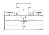
チャネル層20上にバリア層22が設けられる。チャネル層20は、バリア層22のバンドギャップよりも小さなバンドギャップを有することができ、またチャネル層20は、バリア層22よりも大きな電子親和力を有することもできる。バリア層22は、チャネル層20上に堆積させることができる。本発明のいくつかの実施形態では、バリア層22は、約0.1nmから約10nmの間の厚さの、AlN、AlInN、AlGaNまたはAlInGaNである。本発明のいくつかの実施形態による層の例は、文献に記載されている(その開示を、本明細書に完全に記載されているのと同様に、Smorchkova等の、「GROUP-III NITRIDE BASED HIGH ELECTRON MOBILITY TRANSISTOR (HEMT) WITH BARRIER/SPACER LAYER」という名称の、特許文献6参照。)。本発明の特定の諸実施形態では、バリア層22は、オーム接触金属の下に埋め込まれたときに、分極効果によって、チャネル層20とバリア層22の間の境界面で、十分なキャリア濃度を誘起させるのに十分なほど厚く、十分なほど高いAlの組成およびドーピングを有する。またバリア層22は、バリア層22と第2のキャップ層24(図1B)の間の境界面に堆積されたイオン化不純物による、チャネル内での電子の散乱を低減し、または最小限に抑えるのに十分なほど厚くあるべきである。
A
バリア層22は、III族窒化物でよく、チャネル層20のバンドギャップよりも大きなバンドギャップ、およびチャネル層20よりも小さな電子親和力を有する。したがって、本発明のいくつかの実施形態では、バリア層22は、AlGaN、AlInGaN、および/またはAlNまたはそれらの層の組合せである。バリア層22は、例えば、約0.1nmから約10nmの厚さでよいが、亀裂または重大な欠陥の形成をその中で引き起こすほど厚くはない。本発明のいくつかの実施形態では、バリア層22はドープされず、あるいはn型ドーパントで約1019cm−3未満の濃度までドープされる。本発明のいくつかの実施形態では、バリア層22は、AlxGa1−xN(ただし0<x<1)である。特定の諸実施形態では、アルミニウム濃度は約25%である。しかし、本発明の他の諸実施形態では、バリア層22は、アルミニウム濃度が約5%から約100%の間のAlGaNを含む。本発明の特定の諸実施形態では、アルミニウム濃度は約10%を超える。
The
図1Bは、バリア層22上での保護層24の形成を示す。保護層24は、窒化ケイ素(SixNy)、窒化アルミニウム(AlN)、ならびに/あるいは、二酸化ケイ素(SiO2)および/または酸窒化物など、他の適切な保護材料でよい。下にあるバリア層22に損傷を与えずに材料を除去することができる限り、保護層24に他の材料を利用してもよい。例えば、保護層24は、酸化マグネシウム、酸化スカンジウム、酸化アルミニウム、および/または酸窒化アルミニウムを含むこともできる。さらに、保護層24は、組成が一様および/または非一様な、単一の層あるいは複数の層とすることができる。
FIG. 1B shows the formation of the
本発明の特定の諸実施形態では、保護層24はSiNである。SiNはPVDおよび/またはCVDで形成することができ、圧縮歪みまたは引っ張り歪みにおいて非化学量論的でよい。例えば、保護層は、約−100MPaから約100MPaの間の応力を有することができる。本発明のいくつかの実施形態では、SiN保護層は、633nmの波長で約1.6から約2.2の屈折率を有する。特定の諸実施形態では、SiN保護層の屈折率は、1.98±0.05である。
In particular embodiments of the present invention, the
いくつかの実施形態では、保護層24はAlNでよい。AlNは、PVDおよび/またはCVDで形成することができ、圧縮歪みまたは引っ張り歪みにおいて非化学量論的でよい。例えば、保護層は、約−100MPaから約100MPaの間の応力を有することができる。本発明のいくつかの実施形態では、AlN保護層は、633nmの波長で約1.8から約2.1の屈折率を有する。特定の諸実施形態では、AlN保護層の屈折率は、1.85±0.05である。
In some embodiments, the
保護層24はSiO2でもよい。SiO2はPVDおよび/またはCVDで形成することができ、圧縮歪みまたは引っ張り歪みにおいて非化学量論的でよい。例えば、保護層は、約−100MPaから約100MPaの間の応力を有することができる。本発明のいくつかの実施形態では、SiO2保護層は、633nmの波長で約1.36から約1.56の屈折率を有する。特定の諸実施形態では、SiO2保護層の屈折率は、1.46±0.03である。
The
保護層24は、バリア層22上にブランケット形成され、堆積によって形成することができる。例えば、窒化ケイ素層は、高品質なスパッタリングおよび/またはPECVDで形成することができる。一般に、保護層24は、約30nmの厚さを有することができるが、他の厚さの層を利用することもできる。例えば、保護層は、後続のオーム性接触のアニール中に、下にある層を保護するために、十分に厚くなければならない。単層2枚または3枚分ほどの薄い層で、そうした目的に十分となり得る。しかし、一般には、保護層24は約10nmから約500nmの厚さを有することができる。また、III族窒化物層のMOCVD成長を用いて、高品質なSiN保護層をin−situで成長させることもできる。
The
図1Cに示すように、オーム性接触30を形成するために、保護層24にウインドウを開口する。これらのウインドウを、パターニングされたマスクおよびバリア層22に対する低損傷エッチングを利用して形成して、下にあるバリア層22を露出させることができる。低損傷エッチング技術の例には、プラズマに直流成分のない、誘導結合プラズマエッチングまたは電子サイクロトロン共鳴(ECR)エッチングまたはダウンストリームプラズマエッチングなど、反応性イオンエッチング以外のエッチング技術が含まれる。SiO2の場合には、低損傷エッチングは、緩衝フッ化水素酸を用いた湿式エッチングとすることができる。ITO、SCO、MgOなどのエッチングストップ層まで、SiNおよび/またはSiO2を選択的にエッチングし、それに続いて、エッチングストップ層の低損傷除去を実施することもできる。SiNの場合には、エッチングストップ層としてSiO2を使用することができる。そうした諸実施形態では、保護層24は、SiN層、AlN層および/またはSiO2層ならびにエッチングストップ層を含むことができる。したがって、本発明のいくつかの実施形態では、保護層24は複数の層を含むことができる。
As shown in FIG. 1C, a window is opened in the
図1Cにさらに示すように、後続のフォトリソグラフィ段階および蒸着でオーム金属をパターニングして、オーム性接触30を形成する。オーム性接触30は、保護層24内のウインドウよりも小さくなり、その結果、オーム性接触30の縁部が保護層24から離隔されるようにパターニングされる。例えば、オーム性接触30の縁部は、保護層24から約0.1μmから約0.2μmの距離だけ離隔することができる。オーム性接触30は、オーム性接触金属の形成およびパターニング時にずれ公差を許容できるほど十分に大きな距離だけ、保護層24から離隔されるべきである。オーム性接触金属が保護層24に接触すると、後続の加熱段階中に、金属が保護層24内に拡散することがあり、その結果ゲート接点と1つまたは複数のオーム性接触30との間で短絡を生じる恐れがある。ただし、オーム性接触30と保護層24の間の隙間は、保護層24の保護目的を無効にし、それによってデバイスの性能を実質的に低下させるほど大きくあるべきではないが、オーム性材料の、保護層に対する無作為な接触を危うくするほど小さくあるべきでもない。したがって、例えば、本発明のいくつかの実施形態では、隙間は約0.1μmから約0.5μmでよい。
As further shown in FIG. 1C, ohmic metal is patterned in subsequent photolithography steps and depositions to form
オーム性接触材料をアニールして、オーム性接触30を形成する。アニールは、高温アニールでよい。例えば、アニールは、約900℃を超える温度でのアニールでよい。オーム性接触のアニールを使用することによって、オーム性接触の抵抗を、高抵抗から約1Ω−mm未満まで低減させることができる。したがって、本明細書では、「オーム性接触」という用語は、約1Ω−mm未満の接点抵抗を有する、非整流性接点を指す。高温工程段階中に保護層があるため、そうした段階によって引き起こされる恐れのある、バリア層22への損傷を抑制することができる。したがって、例えば、オーム性接触を高温アニールした後のゲート領域21のシート抵抗は、成長させたまま(すなわち、接点をアニールする前)のゲート領域21のシート抵抗と実質的に同じになることができる。
The ohmic contact material is annealed to form the
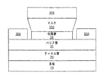
図1Dは、ゲートウインドウの形成を示す。図1Dから分かるように、オーム性接触および保護層24上にマスク26を形成し、パターニングして、保護層24の一部分を露出するウインドウを形成する。次いで、バリア層22の一部分を露出するために、保護層24を貫通して陥凹部を形成する。陥凹部は、上述のように、マスク26および低損傷エッチング法を使用して形成する。オーム性接触30によってソース接点およびドレイン接点が形成される特定の諸実施形態では、陥凹部が、後にはゲート接点32が、ドレイン接点よりもソース接点の方に近くなるように、陥凹部を、ソース接点とドレイン接点の間で位置決めすることができる。
FIG. 1D shows the formation of the gate window. As can be seen in FIG. 1D, a
図1Eから分かるように、ゲート接点32は、陥凹部中に形成され、バリア層22の露出部分に接触する。ゲート接点は、図1Eに示すような「T」ゲートでよく、従来の製作技術を使用して製作することができる。適切なゲート材料は、バリア層の組成によって変わることがあるが、いくつかの実施形態では、Ni、Pt、NiSix、Cu、Pd、Cr、Wおよび/またはWSiNなど、窒化物ベースの半導体材料に対してショットキー接点を形成することのできる従来型の材料を使用することができる。望ましくないことかもしれないが、保護層24とゲート接点32の間の小さな隙間が、例えば、低損傷エッチングの異方性の結果として生じることがあり、それによって保護層24とゲート接点32の間にバリア層22の露出した表面がもたらされる。
As can be seen from FIG. 1E, the
図1Fは、パッシベーション層34の形成を示す。パッシベーション層は、図1Eの構造上にブランケット堆積させることができる。特定の諸実施形態では、パッシベーション層34は、保護層24とオーム接触30の間の隙間を、また保護層24とゲート接点32の間の隙間があればそれも、実質的に埋めるように堆積させる。本発明のいくつかの実施形態では、パッシベーション層34は、窒化ケイ素、窒化アルミニウム、二酸化ケイ素、および/または酸窒化物でよい。さらに、パッシベーション層34は、組成が一様および/または非一様な、単一の層あるいは複数の層とすることができる。
FIG. 1F shows the formation of the
以上、本発明の諸実施形態を、開口したゲート接点ウインドウを形成するための、また保護層24に対する隙間をもつゲート接点を形成するための、2つのマスクによる方法に即して説明してきたが、図2Aおよび図2Bは、オーム性接触ウインドウおよびオーム性接触を単一のマスクで形成するための操作を示す。図2Aから分かるように、保護層24上に、負の斜角をもつ、フォトレジストなどのマスク200を形成することができる。マスク200の負の斜角は、その後形成されるオーム性接触30とパターニングされた保護層24との間の隙間の距離に対応する。保護層24を、上述の低損傷エッチング法を使用して等方的にエッチングして、接点ウインドウを形成する。したがって、接点ウインドウは、マスク200の底辺寸法によって画定される。エッチングが等方性であり、低損傷エッチングにより実質的にオーバーエッチングされて、横方向のアンダカットを所望の間隔にすることができる場合には、負の斜角をもたないマスク層を使用することもできる。
While the embodiments of the present invention have been described in the context of two mask methods for forming an open gate contact window and for forming a gate contact with a gap to the
図2Bから分かるように、オーム接触金属300を、得られた構造上に蒸着させる。マスク200のオーバーハング部が、露出したバリア層22上に金属が堆積される場所を画定する。したがって、接触金属300は、パターニングされた保護層24から離隔される。マスク200およびマスク200上の金属300を除去すると、図1Cの構造がもたらされる。
As can be seen from FIG. 2B, an
図2Aに示す斜角付きのマスクを提供する技術は、当分野の技術者には公知である。さらに、マスク200は斜角を有するように示してあるが、本発明の他の諸実施形態では、マスクは、段を有することもでき、保護層24のエッチングおよび接点材料の堆積用の、2つの異なる見かけのウインドウサイズを有するマスクを形成するような他の構成を有することもできる。したがって、例えば、1回の露光で、保護層24に隣接するフォトレジストの層によって形成されるウインドウの方が、保護層24から離隔されたフォトレジストの層によって形成されるウインドウよりも大きくなるような、オーバーハングまたは段を有するマスクを形成することのできる、異なる露光感度を有する多層フォトレジストを利用することができる。
Techniques for providing the beveled mask shown in FIG. 2A are known to those skilled in the art. Further, although the
図3は、本発明の別の諸実施形態による、トランジスタの製作を示す。図3から分かるように、オーム金属堆積前の保護層24の形成は省略することができ、バリア層22上にオーム金属を堆積させ、パターニングして、バリア層22上にオーム性接触材料領域30を形成することができる。次いで、バリア層22のゲート領域およびオーム性接触材料上に、保護層40を形成する。本発明の特定の諸実施形態では、保護層40は、窒化アルミニウムをスパッタリングによってブランケット堆積させたものでよい。保護層40は、保護層24に関して上記で述べたものなどの材料でもよい。
FIG. 3 illustrates the fabrication of a transistor according to another embodiment of the present invention. As can be seen from FIG. 3, the formation of the
オーム性接触材料領域30のアニールは、保護層40を適切な位置に配置したままで実施する。次いで保護層40を、例えば、上述のような低損傷エッチング技術を使用して除去することができる。次いで、パッシベーション層34の形成前または形成後に、ゲート接点32を形成することができる。例えば、窒化ケイ素層を、スパッタリングによって堆積させることができる。次いで、例えば上述の低損傷エッチング法を使用して、パッシベーション層にゲート陥凹部をエッチングし、陥凹部中にゲートを形成することができる。そのような方法によって、「T」ゲートの縁部に達する十分な厚さを維持する窒化ケイ素パッシベーション層を形成することができる。したがって、図4に示すような構造を有するトランジスタを形成することができる。
The ohmic
あるいは、図4に示す構造は、図1A〜1Fに示す製作段階を利用して形成することもでき、ただし保護層24は、ゲート接点32の形成前または後に除去することができる。そうした場合には、保護層24は、上述のような低損傷エッチング技術を使用して除去すべきである。
Alternatively, the structure shown in FIG. 4 can be formed using the fabrication steps shown in FIGS. 1A-1F, except that the
図5は、保護層24が少なくともオーム性接触30とほぼ同程度の厚さに形成される、本発明の別の諸実施形態を示す。図5から分かるように、そうした諸実施形態では、ゲート接点34の袖部(wing)は、直接保護層24上に形成することができる。例えば、保護層24は、約500から約5000Åの厚さに形成することができる。保護層24を通して低損傷エッチングが実施され、「T」ゲート32が、直接保護層24上に載り、またそれを貫通して形成される。例えば、デバイスの環境からの保護を向上させるために、その後にオーバーレイヤ(overlayer)パッシベーション34を形成することもできる。
FIG. 5 illustrates other embodiments of the present invention in which the
以上、本発明の諸実施形態を、本明細書において特定のHEMT構造に関して説明してきたが、本発明は、そうした構造に限定されるものと解釈すべきではない。例えば、追加の層をHEMTデバイス内に含めても、本発明の教示の恩恵を受けることができる。そうした追加の層は、文献に記載のGaNキャップ層を含むことができる(例えば、非特許文献1または2001年7月12日出願、2002年6月6日公開の、「ALUMINUM GALLIUM NITRIDE/GALLIUM NITRIDE HIGH ELECTRON MOBILITY TRANSISTORS HAVING A GATE CONTACT ON A GALLIUM NITRIDE BASED CAP SEGMENT AND METHODS OF FABRICATING SAME」という名称の特許文献4参照)。いくつかの実施形態では、MISHEMTを製作するために、かつ/または表面を不活性化するために、SiNxや比較的高品質のAlNなどの絶縁層を堆積させることができる。追加の層は、組成が傾斜した1層または複数層の遷移層を含むこともできる。 While embodiments of the present invention have been described herein with reference to particular HEMT structures, the present invention should not be construed as limited to such structures. For example, additional layers can be included in the HEMT device to benefit from the teachings of the present invention. Such additional layers may include the GaN cap layers described in the literature (eg, “ALUMINUM GALLIUM NITRIDE / GALLIUM NITRIDE, filed July 12, 2001, published June 6, 2002). HIGH ELECTRON MOBILITY TRANSISTORS HAVING A GATE CONTACT ON A GALLIUM NITRIDE BASED CAP SEGMENT AND METHODS OF FABRICATING SAME. In some embodiments, an insulating layer such as SiNx or a relatively high quality AlN can be deposited to fabricate a MISHEMT and / or to deactivate the surface. The additional layers can also include one or more transition layers with graded compositions.
さらに、文献に記載されているように、バリア層22が複数の層を備えることもできる(その開示を、本明細書に完全に記載されているのと同様に、参照により本明細書に組み込む、Smorchkova等の、「GROUP-III NITRIDE BASED HIGH ELECTRON MOBILITY TRANSISTOR (HEMT) WITH BARRIER/SPACER LAYER」という名称の特許文献6参照。)。したがって、本発明の諸実施形態では、バリア層は単一の層に限定されるものと解釈すべきではなく、例えばGaN、AlGaNおよび/またはAlN層の組合せを有するバリア層を含むことができる。例えば、GaN、AlN構造を、合金散乱を低減または回避するために利用することができる。したがって、本発明の諸実施形態は、窒化物ベースのバリア層を含むことができ、そうした窒化物ベースのバリア層は、AlGaNベースのバリア層、AlNベースのバリア層、およびそれらの組合せを含むことができる。
Further, as described in the literature, the
以上、図面および明細書で、本発明の一般的な諸実施形態が開示されてきた。特定の用語が用いられてきたが、それらは限定するためではなく、一般的および説明的な意味において使用されたにすぎない。 In the above, drawings and specification, general embodiments of the present invention have been disclosed. Although specific terms have been used, they have been used in a general and descriptive sense only, not for purposes of limitation.
Claims (23)
前記窒化物ベースの半導体バリア層のゲート領域上に、保護層を形成するステップと、
前記バリア層上に、パターニングされた複数のオーム接点金属領域を形成するステップと、
第1および第2のオーム接点を形成するために、前記パターニングされたオーム接点金属を、前記ゲート領域上に前記保護層を載せたままアニールするステップと、
前記保護層全体を除去するステップと、
前記バリア層の前記ゲート領域上に、ゲート接点を形成するステップと
を有することを特徴とするトランジスタを製作する方法。Forming a nitride-based semiconductor barrier layer on the nitride-based semiconductor channel layer;
Forming a protective layer on a gate region of the nitride-based semiconductor barrier layer;
Forming a plurality of patterned ohmic contact metal regions on the barrier layer;
Annealing the patterned ohmic contact metal with the protective layer on the gate region to form first and second ohmic contacts;
Removing the entire protective layer;
Forming a gate contact on the gate region of the barrier layer.
前記バリア層の前記ゲート領域の一部分を露出させるために、低損傷エッチング技術を利用して、前記パッシベーション層に陥凹部をエッチングするステップと、
前記パッシベーション層の前記陥凹部中に、前記ゲート接点を形成するステップと
を含むことを特徴とする請求項5に記載の方法。Forming the gate contact comprises:
Etching a recess in the passivation layer using a low damage etch technique to expose a portion of the gate region of the barrier layer;
6. The method of claim 5, comprising forming the gate contact in the recess of the passivation layer.
前記バリア層上に、保護層材料をブランケット堆積させるステップと、
前記ブランケット堆積させた保護層材料上に、前記第1および第2のオーム接点の位置に対応するウインドウを有するマスクを形成するステップと、
低損傷エッチング技術を利用して、前記ウインドウを通して、前記ブランケット堆積させた保護層をエッチングするステップと、
前記マスクを除去するステップと
を含むことを特徴とする請求項8に記載の方法。Forming the patterned protective layer comprises:
Blanket depositing a protective layer material on the barrier layer;
Forming a mask having a window corresponding to the location of the first and second ohmic contacts on the blanket deposited protective layer material;
Etching the blanket deposited protective layer through the window using a low damage etch technique;
9. The method of claim 8, comprising removing the mask.
前記窒化物ベースのチャネル層を設けるために、前記バッファ層上にIII族窒化物チャネル層を形成するステップと
をさらに有することを特徴とする請求項1に記載の方法。Forming a buffer layer on the substrate;
The method of claim 1, further comprising: forming a group III nitride channel layer on the buffer layer to provide the nitride-based channel layer.
Applications Claiming Priority (3)
| Application Number | Priority Date | Filing Date | Title |
|---|---|---|---|
| US10/758,871 | 2004-01-16 | ||
| US10/758,871 US7045404B2 (en) | 2004-01-16 | 2004-01-16 | Nitride-based transistors with a protective layer and a low-damage recess and methods of fabrication thereof |
| PCT/US2004/031756 WO2005076365A1 (en) | 2004-01-16 | 2004-09-28 | Nitride-based transistors with a protective layer and a low-damage recess and methods of fabrication thereof |
Related Child Applications (1)
| Application Number | Title | Priority Date | Filing Date |
|---|---|---|---|
| JP2011254055A Division JP6050579B2 (en) | 2004-01-16 | 2011-11-21 | Nitride-based transistor with protective layer and low damage recess and method of fabrication |
Publications (2)
| Publication Number | Publication Date |
|---|---|
| JP2007518265A JP2007518265A (en) | 2007-07-05 |
| JP5156235B2 true JP5156235B2 (en) | 2013-03-06 |
Family
ID=34807509
Family Applications (2)
| Application Number | Title | Priority Date | Filing Date |
|---|---|---|---|
| JP2006549235A Active JP5156235B2 (en) | 2004-01-16 | 2004-09-28 | Fabrication method for nitride-based transistors |
| JP2011254055A Active JP6050579B2 (en) | 2004-01-16 | 2011-11-21 | Nitride-based transistor with protective layer and low damage recess and method of fabrication |
Family Applications After (1)
| Application Number | Title | Priority Date | Filing Date |
|---|---|---|---|
| JP2011254055A Active JP6050579B2 (en) | 2004-01-16 | 2011-11-21 | Nitride-based transistor with protective layer and low damage recess and method of fabrication |
Country Status (8)
| Country | Link |
|---|---|
| US (3) | US7045404B2 (en) |
| EP (2) | EP1704597B1 (en) |
| JP (2) | JP5156235B2 (en) |
| KR (2) | KR101123459B1 (en) |
| CN (1) | CN100468770C (en) |
| CA (1) | CA2553669A1 (en) |
| TW (1) | TW200525760A (en) |
| WO (1) | WO2005076365A1 (en) |
Families Citing this family (176)
| Publication number | Priority date | Publication date | Assignee | Title |
|---|---|---|---|---|
| US7112860B2 (en) | 2003-03-03 | 2006-09-26 | Cree, Inc. | Integrated nitride-based acoustic wave devices and methods of fabricating integrated nitride-based acoustic wave devices |
| US7898047B2 (en) * | 2003-03-03 | 2011-03-01 | Samsung Electronics Co., Ltd. | Integrated nitride and silicon carbide-based devices and methods of fabricating integrated nitride-based devices |
| US7045404B2 (en) | 2004-01-16 | 2006-05-16 | Cree, Inc. | Nitride-based transistors with a protective layer and a low-damage recess and methods of fabrication thereof |
| US7382001B2 (en) * | 2004-01-23 | 2008-06-03 | International Rectifier Corporation | Enhancement mode III-nitride FET |
| US7612390B2 (en) * | 2004-02-05 | 2009-11-03 | Cree, Inc. | Heterojunction transistors including energy barriers |
| US20050218414A1 (en) * | 2004-03-30 | 2005-10-06 | Tetsuzo Ueda | 4H-polytype gallium nitride-based semiconductor device on a 4H-polytype substrate |
| JP2005317684A (en) * | 2004-04-27 | 2005-11-10 | Eudyna Devices Inc | Dry etching method and semiconductor device |
| US7332795B2 (en) * | 2004-05-22 | 2008-02-19 | Cree, Inc. | Dielectric passivation for semiconductor devices |
| US7238560B2 (en) * | 2004-07-23 | 2007-07-03 | Cree, Inc. | Methods of fabricating nitride-based transistors with a cap layer and a recessed gate |
| JP4866007B2 (en) * | 2005-01-14 | 2012-02-01 | 富士通株式会社 | Compound semiconductor device |
| JP4845872B2 (en) * | 2005-01-25 | 2011-12-28 | 富士通株式会社 | Semiconductor device having MIS structure and manufacturing method thereof |
| JP4912604B2 (en) * | 2005-03-30 | 2012-04-11 | 住友電工デバイス・イノベーション株式会社 | Nitride semiconductor HEMT and manufacturing method thereof. |
| US7525122B2 (en) * | 2005-06-29 | 2009-04-28 | Cree, Inc. | Passivation of wide band-gap based semiconductor devices with hydrogen-free sputtered nitrides |
| US7855401B2 (en) * | 2005-06-29 | 2010-12-21 | Cree, Inc. | Passivation of wide band-gap based semiconductor devices with hydrogen-free sputtered nitrides |
| US7598576B2 (en) * | 2005-06-29 | 2009-10-06 | Cree, Inc. | Environmentally robust passivation structures for high-voltage silicon carbide semiconductor devices |
| US9331192B2 (en) * | 2005-06-29 | 2016-05-03 | Cree, Inc. | Low dislocation density group III nitride layers on silicon carbide substrates and methods of making the same |
| US20070018198A1 (en) * | 2005-07-20 | 2007-01-25 | Brandes George R | High electron mobility electronic device structures comprising native substrates and methods for making the same |
| US20070018199A1 (en) | 2005-07-20 | 2007-01-25 | Cree, Inc. | Nitride-based transistors and fabrication methods with an etch stop layer |
| US8183595B2 (en) * | 2005-07-29 | 2012-05-22 | International Rectifier Corporation | Normally off III-nitride semiconductor device having a programmable gate |
| JP4897948B2 (en) | 2005-09-02 | 2012-03-14 | 古河電気工業株式会社 | Semiconductor element |
| JP4799965B2 (en) * | 2005-09-06 | 2011-10-26 | 日本電信電話株式会社 | Heterostructure field effect transistor using nitride semiconductor |
| US7638818B2 (en) * | 2005-09-07 | 2009-12-29 | Cree, Inc. | Robust transistors with fluorine treatment |
| US7399692B2 (en) * | 2005-10-03 | 2008-07-15 | International Rectifier Corporation | III-nitride semiconductor fabrication |
| US7709269B2 (en) * | 2006-01-17 | 2010-05-04 | Cree, Inc. | Methods of fabricating transistors including dielectrically-supported gate electrodes |
| US7592211B2 (en) * | 2006-01-17 | 2009-09-22 | Cree, Inc. | Methods of fabricating transistors including supported gate electrodes |
| JP2007234986A (en) * | 2006-03-02 | 2007-09-13 | National Institute Of Information & Communication Technology | Gan field effect transistor including aln barrier layer, and method of manufacturing such field effect transistor |
| JP5362187B2 (en) * | 2006-03-30 | 2013-12-11 | 日本碍子株式会社 | Semiconductor element |
| US9040398B2 (en) * | 2006-05-16 | 2015-05-26 | Cree, Inc. | Method of fabricating seminconductor devices including self aligned refractory contacts |
| US7737455B2 (en) * | 2006-05-19 | 2010-06-15 | Bridgelux, Inc. | Electrode structures for LEDs with increased active area |
| JP5207598B2 (en) * | 2006-05-24 | 2013-06-12 | パナソニック株式会社 | Nitride semiconductor material, semiconductor element and method of manufacturing the same |
| CN100495724C (en) * | 2006-09-06 | 2009-06-03 | 中国科学院半导体研究所 | Gallium nitride radical heterojunction field effect transistor structure and method for making the same |
| JP5520432B2 (en) | 2006-10-03 | 2014-06-11 | 古河電気工業株式会社 | Manufacturing method of semiconductor transistor |
| US8823057B2 (en) | 2006-11-06 | 2014-09-02 | Cree, Inc. | Semiconductor devices including implanted regions for providing low-resistance contact to buried layers and related devices |
| EP2087511B1 (en) * | 2006-11-21 | 2015-03-18 | Imec | Surface treatment and passivation of aigan/gan hemt |
| JP5401758B2 (en) * | 2006-12-12 | 2014-01-29 | サンケン電気株式会社 | Semiconductor device and manufacturing method thereof |
| WO2008086001A2 (en) * | 2007-01-10 | 2008-07-17 | International Rectifier Corporation | Active area shaping for iii-nitride device and process for its manufacture |
| US20080265444A1 (en) * | 2007-04-26 | 2008-10-30 | Heetronix | Thin-film aluminum nitride encapsulant for metallic structures on integrated circuits and method of forming same |
| US9647103B2 (en) * | 2007-05-04 | 2017-05-09 | Sensor Electronic Technology, Inc. | Semiconductor device with modulated field element isolated from gate electrode |
| JP2008288289A (en) * | 2007-05-16 | 2008-11-27 | Oki Electric Ind Co Ltd | Field-effect transistor and its manufacturing method |
| US8455920B2 (en) * | 2007-05-23 | 2013-06-04 | International Rectifier Corporation | III-nitride heterojunction device |
| JP2008306026A (en) * | 2007-06-08 | 2008-12-18 | Eudyna Devices Inc | Method of manufacturing semiconductor device |
| US20090072269A1 (en) * | 2007-09-17 | 2009-03-19 | Chang Soo Suh | Gallium nitride diodes and integrated components |
| US7800132B2 (en) * | 2007-10-25 | 2010-09-21 | Northrop Grumman Systems Corporation | High electron mobility transistor semiconductor device having field mitigating plate and fabrication method thereof |
| US7935620B2 (en) * | 2007-12-05 | 2011-05-03 | Freescale Semiconductor, Inc. | Method for forming semiconductor devices with low leakage Schottky contacts |
| KR100922575B1 (en) * | 2007-12-05 | 2009-10-21 | 한국전자통신연구원 | Semiconductor device with T-gate electrode and method for fabricating thereof |
| US8431962B2 (en) * | 2007-12-07 | 2013-04-30 | Northrop Grumman Systems Corporation | Composite passivation process for nitride FET |
| US7632726B2 (en) * | 2007-12-07 | 2009-12-15 | Northrop Grumman Space & Mission Systems Corp. | Method for fabricating a nitride FET including passivation layers |
| US7750370B2 (en) | 2007-12-20 | 2010-07-06 | Northrop Grumman Space & Mission Systems Corp. | High electron mobility transistor having self-aligned miniature field mitigating plate on a protective dielectric layer |
| US7842587B2 (en) * | 2008-01-30 | 2010-11-30 | Freescale Semiconductor, Inc. | III-V MOSFET fabrication and device |
| US8519438B2 (en) | 2008-04-23 | 2013-08-27 | Transphorm Inc. | Enhancement mode III-N HEMTs |
| US9711633B2 (en) * | 2008-05-09 | 2017-07-18 | Cree, Inc. | Methods of forming group III-nitride semiconductor devices including implanting ions directly into source and drain regions and annealing to activate the implanted ions |
| US7985986B2 (en) | 2008-07-31 | 2011-07-26 | Cree, Inc. | Normally-off semiconductor devices |
| US8384115B2 (en) | 2008-08-01 | 2013-02-26 | Cree, Inc. | Bond pad design for enhancing light extraction from LED chips |
| US8289065B2 (en) | 2008-09-23 | 2012-10-16 | Transphorm Inc. | Inductive load power switching circuits |
| US7898004B2 (en) | 2008-12-10 | 2011-03-01 | Transphorm Inc. | Semiconductor heterostructure diodes |
| WO2010122628A1 (en) | 2009-04-20 | 2010-10-28 | 富士通株式会社 | Compound semiconductor device and method for manufacturing the same |
| US8742459B2 (en) * | 2009-05-14 | 2014-06-03 | Transphorm Inc. | High voltage III-nitride semiconductor devices |
| US8105889B2 (en) | 2009-07-27 | 2012-01-31 | Cree, Inc. | Methods of fabricating transistors including self-aligned gate electrodes and source/drain regions |
| US8390000B2 (en) | 2009-08-28 | 2013-03-05 | Transphorm Inc. | Semiconductor devices with field plates |
| US20110068348A1 (en) | 2009-09-18 | 2011-03-24 | Taiwan Semiconductor Manufacturing Company, Ltd. | Thin body mosfet with conducting surface channel extensions and gate-controlled channel sidewalls |
| US8216924B2 (en) * | 2009-10-16 | 2012-07-10 | Cree, Inc. | Methods of fabricating transistors using laser annealing of source/drain regions |
| US8389977B2 (en) | 2009-12-10 | 2013-03-05 | Transphorm Inc. | Reverse side engineered III-nitride devices |
| US20110241020A1 (en) * | 2010-03-31 | 2011-10-06 | Triquint Semiconductor, Inc. | High electron mobility transistor with recessed barrier layer |
| US8907350B2 (en) * | 2010-04-28 | 2014-12-09 | Cree, Inc. | Semiconductor devices having improved adhesion and methods of fabricating the same |
| US8847563B2 (en) | 2010-07-15 | 2014-09-30 | Cree, Inc. | Power converter circuits including high electron mobility transistors for switching and rectifcation |
| US8742460B2 (en) | 2010-12-15 | 2014-06-03 | Transphorm Inc. | Transistors with isolation regions |
| US8643062B2 (en) | 2011-02-02 | 2014-02-04 | Transphorm Inc. | III-N device structures and methods |
| JP5762049B2 (en) * | 2011-02-28 | 2015-08-12 | ルネサスエレクトロニクス株式会社 | Semiconductor device |
| US8772842B2 (en) | 2011-03-04 | 2014-07-08 | Transphorm, Inc. | Semiconductor diodes with low reverse bias currents |
| US8716141B2 (en) | 2011-03-04 | 2014-05-06 | Transphorm Inc. | Electrode configurations for semiconductor devices |
| KR101781438B1 (en) * | 2011-06-14 | 2017-09-25 | 삼성전자주식회사 | Fabrication method of semiconductor light emitting device |
| US8901604B2 (en) | 2011-09-06 | 2014-12-02 | Transphorm Inc. | Semiconductor devices with guard rings |
| US9257547B2 (en) | 2011-09-13 | 2016-02-09 | Transphorm Inc. | III-N device structures having a non-insulating substrate |
| US8598937B2 (en) | 2011-10-07 | 2013-12-03 | Transphorm Inc. | High power semiconductor electronic components with increased reliability |
| US8530978B1 (en) * | 2011-12-06 | 2013-09-10 | Hrl Laboratories, Llc | High current high voltage GaN field effect transistors and method of fabricating same |
| JP2013131650A (en) * | 2011-12-21 | 2013-07-04 | Fujitsu Ltd | Semiconductor device and method of manufacturing the same |
| US9165766B2 (en) | 2012-02-03 | 2015-10-20 | Transphorm Inc. | Buffer layer structures suited for III-nitride devices with foreign substrates |
| US8860088B2 (en) * | 2012-02-23 | 2014-10-14 | Taiwan Semiconductor Manufacturing Company, Ltd. | Semiconductor structure and method of forming the same |
| US9093366B2 (en) | 2012-04-09 | 2015-07-28 | Transphorm Inc. | N-polar III-nitride transistors |
| CN102709321A (en) * | 2012-04-20 | 2012-10-03 | 程凯 | Enhanced switch element and production method thereof |
| US20130299895A1 (en) | 2012-05-09 | 2013-11-14 | Taiwan Semiconductor Manufacturing Co., Ltd. | Iii-v compound semiconductor device having dopant layer and method of making the same |
| US8866195B2 (en) * | 2012-07-06 | 2014-10-21 | Taiwan Semiconductor Manufacturing Co., Ltd. | III-V compound semiconductor device having metal contacts and method of making the same |
| US9184275B2 (en) | 2012-06-27 | 2015-11-10 | Transphorm Inc. | Semiconductor devices with integrated hole collectors |
| US9076850B2 (en) | 2012-07-30 | 2015-07-07 | Samsung Electronics Co., Ltd. | High electron mobility transistor |
| US9099490B2 (en) * | 2012-09-28 | 2015-08-04 | Intel Corporation | Self-aligned structures and methods for asymmetric GaN transistors and enhancement mode operation |
| US9991399B2 (en) | 2012-10-04 | 2018-06-05 | Cree, Inc. | Passivation structure for semiconductor devices |
| US8994073B2 (en) | 2012-10-04 | 2015-03-31 | Cree, Inc. | Hydrogen mitigation schemes in the passivation of advanced devices |
| US9812338B2 (en) | 2013-03-14 | 2017-11-07 | Cree, Inc. | Encapsulation of advanced devices using novel PECVD and ALD schemes |
| JP6178065B2 (en) * | 2012-10-09 | 2017-08-09 | 株式会社東芝 | Semiconductor device |
| JP6486828B2 (en) | 2012-11-16 | 2019-03-20 | マサチューセッツ インスティテュート オブ テクノロジー | Etching technology for semiconductor structure and recess formation |
| CN105164811B (en) | 2013-02-15 | 2018-08-31 | 创世舫电子有限公司 | Electrode of semiconductor devices and forming method thereof |
| US9087718B2 (en) | 2013-03-13 | 2015-07-21 | Transphorm Inc. | Enhancement-mode III-nitride devices |
| US9245993B2 (en) | 2013-03-15 | 2016-01-26 | Transphorm Inc. | Carbon doping semiconductor devices |
| US20140335666A1 (en) | 2013-05-13 | 2014-11-13 | The Government Of The United States Of America, As Represented By The Secretary Of The Navy | Growth of High-Performance III-Nitride Transistor Passivation Layer for GaN Electronics |
| US9755059B2 (en) | 2013-06-09 | 2017-09-05 | Cree, Inc. | Cascode structures with GaN cap layers |
| US9679981B2 (en) | 2013-06-09 | 2017-06-13 | Cree, Inc. | Cascode structures for GaN HEMTs |
| US9847411B2 (en) | 2013-06-09 | 2017-12-19 | Cree, Inc. | Recessed field plate transistor structures |
| US9443938B2 (en) | 2013-07-19 | 2016-09-13 | Transphorm Inc. | III-nitride transistor including a p-type depleting layer |
| JP6338832B2 (en) * | 2013-07-31 | 2018-06-06 | ルネサスエレクトロニクス株式会社 | Semiconductor device |
| KR101455283B1 (en) * | 2013-08-09 | 2014-10-31 | 홍익대학교 산학협력단 | FORMING METHOD FOR PASSIVATION FILM AND MANUFACTURING METHOD FOR AlGaN/GaN HFET INCLUDING THE FORMING METHOD |
| CN103760206B (en) * | 2014-01-14 | 2016-07-06 | 江苏新广联科技股份有限公司 | Blood glucose test chip based on gallium nitride material |
| US20150255589A1 (en) * | 2014-03-10 | 2015-09-10 | Toshiba Corporation | Indium-containing contact and barrier layer for iii-nitride high electron mobility transistor devices |
| EP2930754A1 (en) * | 2014-04-11 | 2015-10-14 | Nxp B.V. | Semiconductor device |
| US10276712B2 (en) | 2014-05-29 | 2019-04-30 | Hrl Laboratories, Llc | III-nitride field-effect transistor with dual gates |
| US9318593B2 (en) | 2014-07-21 | 2016-04-19 | Transphorm Inc. | Forming enhancement mode III-nitride devices |
| US9536966B2 (en) | 2014-12-16 | 2017-01-03 | Transphorm Inc. | Gate structures for III-N devices |
| US9536967B2 (en) | 2014-12-16 | 2017-01-03 | Transphorm Inc. | Recessed ohmic contacts in a III-N device |
| CN106373874A (en) * | 2015-07-21 | 2017-02-01 | 北大方正集团有限公司 | Manufacturing method of ohmic contact electrode based on AlGaN/GaN HEMT |
| US9812532B1 (en) | 2015-08-28 | 2017-11-07 | Hrl Laboratories, Llc | III-nitride P-channel transistor |
| CN105226093B (en) * | 2015-11-11 | 2018-06-26 | 成都海威华芯科技有限公司 | GaN HEMT devices and preparation method thereof |
| EP3378097A4 (en) | 2015-11-19 | 2019-09-11 | HRL Laboratories, LLC | Iii-nitride field-effect transistor with dual gates |
| CN105448977A (en) * | 2015-12-31 | 2016-03-30 | 深圳市华讯方舟微电子科技有限公司 | High electron mobility transistor and fabrication method thereof |
| WO2017123999A1 (en) | 2016-01-15 | 2017-07-20 | Transphorm Inc. | Enhancement mode iii-nitride devices having an al(1-x)sixo gate insulator |
| US10128365B2 (en) | 2016-03-17 | 2018-11-13 | Cree, Inc. | Bypassed gate transistors having improved stability |
| US9786660B1 (en) | 2016-03-17 | 2017-10-10 | Cree, Inc. | Transistor with bypassed gate structure field |
| US9947616B2 (en) | 2016-03-17 | 2018-04-17 | Cree, Inc. | High power MMIC devices having bypassed gate transistors |
| CN107230617A (en) * | 2016-03-25 | 2017-10-03 | 北京大学 | The preparation method of gallium nitride semiconductor device |
| TWI762486B (en) | 2016-05-31 | 2022-05-01 | 美商創世舫科技有限公司 | Iii-nitride devices including a graded depleting layer |
| US10354879B2 (en) | 2016-06-24 | 2019-07-16 | Cree, Inc. | Depletion mode semiconductor devices including current dependent resistance |
| US10804386B2 (en) * | 2016-07-01 | 2020-10-13 | Intel Corporation | Gate stack design for GaN e-mode transistor performance |
| CN108010840B (en) * | 2016-11-02 | 2021-04-23 | 株洲中车时代半导体有限公司 | Method for manufacturing doped semiconductor device and semiconductor device |
| JP2018170458A (en) * | 2017-03-30 | 2018-11-01 | 株式会社東芝 | High output device |
| CN107424919A (en) * | 2017-05-12 | 2017-12-01 | 中国电子科技集团公司第十三研究所 | A kind of low Damage Medium grid and preparation method thereof |
| US10615273B2 (en) | 2017-06-21 | 2020-04-07 | Cree, Inc. | Semiconductor devices having a plurality of unit cell transistors that have smoothed turn-on behavior and improved linearity |
| US10268789B1 (en) | 2017-10-03 | 2019-04-23 | Cree, Inc. | Transistor amplifiers having node splitting for loop stability and related methods |
| CN111466012B (en) * | 2017-10-11 | 2023-09-29 | 阿卜杜拉国王科技大学 | Semiconductor device having heterojunction of indium gallium nitride ternary alloy layer and second group III nitride ternary alloy layer |
| CN109728086A (en) * | 2017-10-31 | 2019-05-07 | 中国工程物理研究院电子工程研究所 | The preparation method of side wall grid high mobility transistor |
| JP7100241B2 (en) * | 2017-12-20 | 2022-07-13 | 富士通株式会社 | Compound semiconductor device and its manufacturing method |
| CN108461543B (en) * | 2018-05-29 | 2022-07-08 | 苏州闻颂智能科技有限公司 | GaN HEMT device and preparation method thereof |
| US10483352B1 (en) * | 2018-07-11 | 2019-11-19 | Cree, Inc. | High power transistor with interior-fed gate fingers |
| US10763334B2 (en) | 2018-07-11 | 2020-09-01 | Cree, Inc. | Drain and/or gate interconnect and finger structure |
| US10600746B2 (en) | 2018-07-19 | 2020-03-24 | Cree, Inc. | Radio frequency transistor amplifiers and other multi-cell transistors having gaps and/or isolation structures between groups of unit cell transistors |
| WO2020106537A1 (en) | 2018-11-19 | 2020-05-28 | Cree, Inc. | Semiconductor devices having a plurality of unit cell transistors that have smoothed turn-on behavior and improved linearity |
| US10770415B2 (en) | 2018-12-04 | 2020-09-08 | Cree, Inc. | Packaged transistor devices with input-output isolation and methods of forming packaged transistor devices with input-output isolation |
| US10741496B2 (en) | 2018-12-04 | 2020-08-11 | Nxp Usa, Inc. | Semiconductor devices with a protection layer and methods of fabrication |
| JP7074045B2 (en) * | 2018-12-21 | 2022-05-24 | 住友電気工業株式会社 | Nitride semiconductor device manufacturing method and nitride semiconductor device |
| US10937873B2 (en) | 2019-01-03 | 2021-03-02 | Cree, Inc. | High electron mobility transistors having improved drain current drift and/or leakage current performance |
| JP7163806B2 (en) * | 2019-02-05 | 2022-11-01 | 富士通株式会社 | Compound semiconductor device, method for manufacturing compound semiconductor device, and amplifier |
| CN109841677A (en) * | 2019-03-28 | 2019-06-04 | 英诺赛科(珠海)科技有限公司 | High electron mobility transistor and its manufacturing method |
| US11417746B2 (en) | 2019-04-24 | 2022-08-16 | Wolfspeed, Inc. | High power transistor with interior-fed fingers |
| US10971612B2 (en) | 2019-06-13 | 2021-04-06 | Cree, Inc. | High electron mobility transistors and power amplifiers including said transistors having improved performance and reliability |
| US10923585B2 (en) | 2019-06-13 | 2021-02-16 | Cree, Inc. | High electron mobility transistors having improved contact spacing and/or improved contact vias |
| CN112436056B (en) * | 2019-08-26 | 2024-03-26 | 联华电子股份有限公司 | High electron mobility transistor |
| CN112490286B (en) * | 2019-09-12 | 2023-09-19 | 联华电子股份有限公司 | Semiconductor device and method for manufacturing the same |
| US11075271B2 (en) | 2019-10-14 | 2021-07-27 | Cree, Inc. | Stepped field plates with proximity to conduction channel and related fabrication methods |
| US11658233B2 (en) | 2019-11-19 | 2023-05-23 | Wolfspeed, Inc. | Semiconductors with improved thermal budget and process of making semiconductors with improved thermal budget |
| CN111223925A (en) * | 2019-11-27 | 2020-06-02 | 西安电子科技大学 | Bidirectional blocking power device based on AlN/GaN superlattice channel and manufacturing method |
| JP2023520028A (en) | 2020-04-03 | 2023-05-15 | ウルフスピード インコーポレイテッド | III-Nitride based high frequency transistor amplifier with source, gate and/or drain conductive vias |
| JP2023520029A (en) | 2020-04-03 | 2023-05-15 | ウルフスピード インコーポレイテッド | III-Nitride based high frequency amplifier with backside source, gate and/or drain terminals |
| US11670605B2 (en) | 2020-04-03 | 2023-06-06 | Wolfspeed, Inc. | RF amplifier devices including interconnect structures and methods of manufacturing |
| US11356070B2 (en) | 2020-06-01 | 2022-06-07 | Wolfspeed, Inc. | RF amplifiers having shielded transmission line structures |
| US11837457B2 (en) | 2020-09-11 | 2023-12-05 | Wolfspeed, Inc. | Packaging for RF transistor amplifiers |
| US20210313293A1 (en) | 2020-04-03 | 2021-10-07 | Cree, Inc. | Rf amplifier devices and methods of manufacturing |
| US11769768B2 (en) | 2020-06-01 | 2023-09-26 | Wolfspeed, Inc. | Methods for pillar connection on frontside and passive device integration on backside of die |
| US11228287B2 (en) | 2020-06-17 | 2022-01-18 | Cree, Inc. | Multi-stage decoupling networks integrated with on-package impedance matching networks for RF power amplifiers |
| US11533025B2 (en) | 2020-06-18 | 2022-12-20 | Wolfspeed, Inc. | Integrated doherty amplifier with added isolation between the carrier and the peaking transistors |
| US11533024B2 (en) | 2020-06-25 | 2022-12-20 | Wolfspeed, Inc. | Multi-zone radio frequency transistor amplifiers |
| US11581859B2 (en) | 2020-06-26 | 2023-02-14 | Wolfspeed, Inc. | Radio frequency (RF) transistor amplifier packages with improved isolation and lead configurations |
| CN112335039B (en) * | 2020-07-08 | 2021-12-10 | 英诺赛科(珠海)科技有限公司 | Electronic device and method for manufacturing the same |
| US11887945B2 (en) | 2020-09-30 | 2024-01-30 | Wolfspeed, Inc. | Semiconductor device with isolation and/or protection structures |
| US11742302B2 (en) | 2020-10-23 | 2023-08-29 | Wolfspeed, Inc. | Electronic device packages with internal moisture barriers |
| US20220157671A1 (en) | 2020-11-13 | 2022-05-19 | Cree, Inc. | Packaged rf power device with pcb routing |
| US11791389B2 (en) | 2021-01-08 | 2023-10-17 | Wolfspeed, Inc. | Radio frequency transistor amplifiers having widened and/or asymmetric source/drain regions for improved on-resistance performance |
| CN114975614A (en) * | 2021-02-24 | 2022-08-30 | 联华电子股份有限公司 | High electron mobility transistor and manufacturing method thereof |
| US11869964B2 (en) * | 2021-05-20 | 2024-01-09 | Wolfspeed, Inc. | Field effect transistors with modified access regions |
| US20220376085A1 (en) | 2021-05-20 | 2022-11-24 | Cree, Inc. | Methods of manufacturing high electron mobility transistors having improved performance |
| TWI762346B (en) * | 2021-06-04 | 2022-04-21 | 瑞礱科技股份有限公司 | A kind of ohmic contact manufacturing method of group III nitride semiconductor element |
| US11842937B2 (en) | 2021-07-30 | 2023-12-12 | Wolfspeed, Inc. | Encapsulation stack for improved humidity performance and related fabrication methods |
| US20230075505A1 (en) | 2021-09-03 | 2023-03-09 | Wolfspeed, Inc. | Metal pillar connection topologies for heterogeneous packaging |
| US20230078017A1 (en) | 2021-09-16 | 2023-03-16 | Wolfspeed, Inc. | Semiconductor device incorporating a substrate recess |
| WO2023056145A1 (en) | 2021-10-01 | 2023-04-06 | Wolfspeed, Inc. | Bypassed gate transistors having improved stability |
| US20230291367A1 (en) | 2022-03-08 | 2023-09-14 | Wolfspeed, Inc. | Group iii nitride-based monolithic microwave integrated circuits having multi-layer metal-insulator-metal capacitors |
| US20240106397A1 (en) | 2022-09-23 | 2024-03-28 | Wolfspeed, Inc. | Transistor amplifier with pcb routing and surface mounted transistor die |
| US20240105824A1 (en) | 2022-09-23 | 2024-03-28 | Wolfspeed, Inc. | Barrier Structure for Sub-100 Nanometer Gate Length Devices |
| US20240105823A1 (en) | 2022-09-23 | 2024-03-28 | Wolfspeed, Inc. | Barrier Structure for Dispersion Reduction in Transistor Devices |
| US20240120202A1 (en) | 2022-10-06 | 2024-04-11 | Wolfspeed, Inc. | Implanted Regions for Semiconductor Structures with Deep Buried Layers |
Family Cites Families (164)
| Publication number | Priority date | Publication date | Assignee | Title |
|---|---|---|---|---|
| US34861A (en) * | 1862-04-01 | Improved washing-machine | ||
| FR1487060A (en) * | 1965-07-30 | 1967-10-11 | ||
| FR2465317A2 (en) | 1979-03-28 | 1981-03-20 | Thomson Csf | FIELD EFFECT TRANSISTOR WITH HIGH BREAKAGE FREQUENCY |
| DE3072175D1 (en) | 1979-12-28 | 1990-04-26 | Fujitsu Ltd | SEMICONDUCTOR DEVICES WITH HETEROUITION. |
| US4551905A (en) * | 1982-12-09 | 1985-11-12 | Cornell Research Foundation, Inc. | Fabrication of metal lines for semiconductor devices |
| US4536942A (en) * | 1982-12-09 | 1985-08-27 | Cornell Research Foundation, Inc. | Fabrication of T-shaped metal lines for semiconductor devices |
| JPH088350B2 (en) | 1985-04-08 | 1996-01-29 | 日本電気株式会社 | Semiconductor device |
| US4987008A (en) * | 1985-07-02 | 1991-01-22 | Semiconductor Energy Laboratory Co., Ltd. | Thin film formation method |
| JPS6229175A (en) * | 1985-07-29 | 1987-02-07 | Nippon Telegr & Teleph Corp <Ntt> | Manufacture of field effect type transistor |
| US4755867A (en) | 1986-08-15 | 1988-07-05 | American Telephone And Telegraph Company, At&T Bell Laboratories | Vertical Enhancement-mode Group III-V compound MISFETs |
| US4788156A (en) | 1986-09-24 | 1988-11-29 | Microwave Technology, Inc. | Subchannel doping to reduce short-gate effects in field effect transistors |
| JPS63155671A (en) * | 1986-12-18 | 1988-06-28 | Nec Corp | Manufacture of semiconductor device |
| US4987462A (en) * | 1987-01-06 | 1991-01-22 | Texas Instruments Incorporated | Power MISFET |
| US5258631A (en) * | 1987-01-30 | 1993-11-02 | Hitachi, Ltd. | Semiconductor device having a two-dimensional electron gas as an active layer |
| US4792531A (en) * | 1987-10-05 | 1988-12-20 | Menlo Industries, Inc. | Self-aligned gate process |
| US4866005A (en) | 1987-10-26 | 1989-09-12 | North Carolina State University | Sublimation of silicon carbide to produce large, device quality single crystals of silicon carbide |
| US5411914A (en) | 1988-02-19 | 1995-05-02 | Massachusetts Institute Of Technology | III-V based integrated circuits having low temperature growth buffer or passivation layers |
| EP0334006A1 (en) | 1988-02-22 | 1989-09-27 | Siemens Aktiengesellschaft | Stacked channel heterojunction fet |
| JP2508818B2 (en) * | 1988-10-03 | 1996-06-19 | 三菱電機株式会社 | Method for manufacturing semiconductor device |
| US5231038A (en) * | 1989-04-04 | 1993-07-27 | Mitsubishi Denki Kabushiki Kaisha | Method of producing field effect transistor |
| US4946547A (en) | 1989-10-13 | 1990-08-07 | Cree Research, Inc. | Method of preparing silicon carbide surfaces for crystal growth |
| US5053348A (en) | 1989-12-01 | 1991-10-01 | Hughes Aircraft Company | Fabrication of self-aligned, t-gate hemt |
| US5196358A (en) * | 1989-12-29 | 1993-03-23 | The United States Of America As Represented By The Secretary Of The Navy | Method of manufacturing InP junction FETS and junction HEMTS using dual implantation and double nitride layers |
| JPH03292744A (en) * | 1990-01-24 | 1991-12-24 | Toshiba Corp | Compound semiconductor device and manufacture thereof |
| US5210051A (en) | 1990-03-27 | 1993-05-11 | Cree Research, Inc. | High efficiency light emitting diodes from bipolar gallium nitride |
| US5172197A (en) | 1990-04-11 | 1992-12-15 | Hughes Aircraft Company | Hemt structure with passivated donor layer |
| US5292501A (en) | 1990-06-25 | 1994-03-08 | Degenhardt Charles R | Use of a carboxy-substituted polymer to inhibit plaque formation without tooth staining |
| US5200022A (en) | 1990-10-03 | 1993-04-06 | Cree Research, Inc. | Method of improving mechanically prepared substrate surfaces of alpha silicon carbide for deposition of beta silicon carbide thereon and resulting product |
| JPH04167439A (en) * | 1990-10-30 | 1992-06-15 | Mitsubishi Electric Corp | Manufacture of semiconductor device |
| JPH04223342A (en) * | 1990-12-26 | 1992-08-13 | Mitsubishi Electric Corp | Gate electrode of semiconductor device and manufacture thereof |
| US5192987A (en) | 1991-05-17 | 1993-03-09 | Apa Optics, Inc. | High electron mobility transistor with GaN/Alx Ga1-x N heterojunctions |
| JP3135939B2 (en) * | 1991-06-20 | 2001-02-19 | 富士通株式会社 | HEMT type semiconductor device |
| JPH0575139A (en) * | 1991-09-12 | 1993-03-26 | Mitsubishi Electric Corp | Semiconductor device and manufacture thereof |
| JP2735718B2 (en) * | 1991-10-29 | 1998-04-02 | 三菱電機株式会社 | Compound semiconductor device and method of manufacturing the same |
| JP3352712B2 (en) | 1991-12-18 | 2002-12-03 | 浩 天野 | Gallium nitride based semiconductor device and method of manufacturing the same |
| DE69202554T2 (en) | 1991-12-25 | 1995-10-19 | Nec Corp | Tunnel transistor and its manufacturing process. |
| JP2978972B2 (en) * | 1992-03-12 | 1999-11-15 | 富士通株式会社 | Method for manufacturing semiconductor device |
| JPH05275463A (en) | 1992-03-30 | 1993-10-22 | Matsushita Electric Ind Co Ltd | Semiconductor device |
| JPH05299441A (en) * | 1992-04-24 | 1993-11-12 | Matsushita Electric Ind Co Ltd | Manufacture of field effect transistor |
| JPH05326561A (en) | 1992-05-22 | 1993-12-10 | Nec Corp | Manufacture of field effect transistor |
| JPH0653241A (en) * | 1992-08-03 | 1994-02-25 | Nec Corp | Manufacture of field effect transistor |
| EP0592064B1 (en) * | 1992-08-19 | 1998-09-23 | Mitsubishi Denki Kabushiki Kaisha | Method of producing a field effect transistor |
| US5399896A (en) * | 1992-09-29 | 1995-03-21 | Mitsubishi Denki Kabushiki Kaisha | FET with a T-shaped gate of a particular structure |
| JPH06267991A (en) | 1993-03-12 | 1994-09-22 | Hitachi Ltd | Semiconductor device and its manufacture |
| JPH06275655A (en) * | 1993-03-24 | 1994-09-30 | Mitsubishi Electric Corp | Semiconductor device and its manufacture |
| DE4326714A1 (en) * | 1993-08-03 | 1995-02-09 | Mantis Ulv Spruehgeraete | Segment rotating nozzle |
| JP2560993B2 (en) * | 1993-09-07 | 1996-12-04 | 日本電気株式会社 | Method for manufacturing compound semiconductor device |
| JPH0786310A (en) * | 1993-09-20 | 1995-03-31 | Mitsubishi Electric Corp | Method for forming metal gate electrode having high melting point |
| US5393993A (en) | 1993-12-13 | 1995-02-28 | Cree Research, Inc. | Buffer structure between silicon carbide and gallium nitride and resulting semiconductor devices |
| JP3294411B2 (en) * | 1993-12-28 | 2002-06-24 | 富士通株式会社 | Method for manufacturing semiconductor device |
| US5484740A (en) * | 1994-06-06 | 1996-01-16 | Motorola, Inc. | Method of manufacturing a III-V semiconductor gate structure |
| US5514605A (en) * | 1994-08-24 | 1996-05-07 | Nec Corporation | Fabrication process for compound semiconductor device |
| US5686737A (en) | 1994-09-16 | 1997-11-11 | Cree Research, Inc. | Self-aligned field-effect transistor for high frequency applications |
| US5523589A (en) | 1994-09-20 | 1996-06-04 | Cree Research, Inc. | Vertical geometry light emitting diode with group III nitride active layer and extended lifetime |
| US5592501A (en) | 1994-09-20 | 1997-01-07 | Cree Research, Inc. | Low-strain laser structures with group III nitride active layers |
| US5773334A (en) * | 1994-09-26 | 1998-06-30 | Toyota Jidosha Kabushiki Kaisha | Method of manufacturing a semiconductor device |
| JP3380344B2 (en) * | 1994-11-30 | 2003-02-24 | 富士通株式会社 | Semiconductor device and manufacturing method thereof |
| JP3157690B2 (en) | 1995-01-19 | 2001-04-16 | 沖電気工業株式会社 | Method for manufacturing pn junction element |
| JP2687917B2 (en) * | 1995-02-20 | 1997-12-08 | 日本電気株式会社 | Method for manufacturing semiconductor device |
| US5534462A (en) | 1995-02-24 | 1996-07-09 | Motorola, Inc. | Method for forming a plug and semiconductor device having the same |
| US5670798A (en) | 1995-03-29 | 1997-09-23 | North Carolina State University | Integrated heterostructures of Group III-V nitride semiconductor materials including epitaxial ohmic contact non-nitride buffer layer and methods of fabricating same |
| SE9501311D0 (en) | 1995-04-10 | 1995-04-10 | Abb Research Ltd | Method of producing a semiconductor device having a semiconductor layer of SiC |
| US6002148A (en) | 1995-06-30 | 1999-12-14 | Motorola, Inc. | Silicon carbide transistor and method |
| US5569943A (en) * | 1995-09-01 | 1996-10-29 | The United States Of America As Represented By The Secretary Of The Army | Field effect real space transistor |
| US5733806A (en) * | 1995-09-05 | 1998-03-31 | Motorola, Inc. | Method for forming a self-aligned semiconductor device |
| US6075262A (en) * | 1995-09-21 | 2000-06-13 | Fujitsu Limited | Semiconductor device having T-shaped gate electrode |
| JPH09129865A (en) * | 1995-11-06 | 1997-05-16 | Mitsubishi Electric Corp | Semiconductor device |
| JPH09139494A (en) * | 1995-11-16 | 1997-05-27 | Mitsubishi Electric Corp | Semiconductor device and its manufacture |
| KR0175030B1 (en) * | 1995-12-07 | 1999-04-01 | 김광호 | High heat-resistant metal wiring structure of semiconductor device and method of forming the same |
| KR100195269B1 (en) | 1995-12-22 | 1999-06-15 | 윤종용 | Manufacture method of liquid crystal display device |
| US5915164A (en) | 1995-12-28 | 1999-06-22 | U.S. Philips Corporation | Methods of making high voltage GaN-A1N based semiconductor devices |
| JPH09186175A (en) * | 1995-12-28 | 1997-07-15 | Sanyo Electric Co Ltd | Compd. semiconductor device manufacturing method |
| KR0179116B1 (en) * | 1995-12-30 | 1999-03-20 | 구자홍 | Method for manufacturing self-aligned t-type gate |
| DE19600116C2 (en) | 1996-01-03 | 2001-03-15 | Siemens Ag | Double heterostructure HEMT |
| US5710449A (en) * | 1996-05-22 | 1998-01-20 | Integrated Device Technology, Inc. | Memory cell having active regions without N+ implants |
| JPH1050982A (en) | 1996-07-31 | 1998-02-20 | Nippon Telegr & Teleph Corp <Ntt> | Semiconductor device |
| JP2891204B2 (en) * | 1996-09-27 | 1999-05-17 | 日本電気株式会社 | Method for manufacturing semiconductor device |
| US6936839B2 (en) | 1996-10-16 | 2005-08-30 | The University Of Connecticut | Monolithic integrated circuit including a waveguide and quantum well inversion channel devices and a method of fabricating same |
| US5929467A (en) * | 1996-12-04 | 1999-07-27 | Sony Corporation | Field effect transistor with nitride compound |
| JP2904167B2 (en) * | 1996-12-18 | 1999-06-14 | 日本電気株式会社 | Method for manufacturing semiconductor device |
| US6677619B1 (en) | 1997-01-09 | 2004-01-13 | Nichia Chemical Industries, Ltd. | Nitride semiconductor device |
| JP3156620B2 (en) * | 1997-02-12 | 2001-04-16 | 日本電気株式会社 | Field effect transistor and method of manufacturing the same |
| JP3546634B2 (en) | 1997-03-19 | 2004-07-28 | ソニー株式会社 | Selective etching method for nitride-based compound semiconductor and method for manufacturing semiconductor device |
| JP3670104B2 (en) | 1997-03-27 | 2005-07-13 | 日世株式会社 | Method for producing sterilized food |
| US6448648B1 (en) | 1997-03-27 | 2002-09-10 | The United States Of America As Represented By The Secretary Of The Navy | Metalization of electronic semiconductor devices |
| JPH10335637A (en) | 1997-05-30 | 1998-12-18 | Sony Corp | Hetero-junction field effect transistor |
| US6316820B1 (en) * | 1997-07-25 | 2001-11-13 | Hughes Electronics Corporation | Passivation layer and process for semiconductor devices |
| JPH1154527A (en) * | 1997-07-30 | 1999-02-26 | Fujitsu Ltd | Field effect transistor and its manufacture |
| KR100307986B1 (en) * | 1997-08-28 | 2002-05-09 | 가네꼬 히사시 | Method of manufacturing semiconductor device |
| US6242327B1 (en) * | 1997-09-19 | 2001-06-05 | Fujitsu Limited | Compound semiconductor device having a reduced source resistance |
| US6201262B1 (en) | 1997-10-07 | 2001-03-13 | Cree, Inc. | Group III nitride photonic devices on silicon carbide substrates with conductive buffer interlay structure |
| JP3372470B2 (en) | 1998-01-20 | 2003-02-04 | シャープ株式会社 | Nitride III-V compound semiconductor device |
| EP0974160A1 (en) * | 1998-02-09 | 2000-01-26 | Koninklijke Philips Electronics N.V. | Process of manufacturing a semiconductor device including a buried channel field effect transistor |
| US6150680A (en) | 1998-03-05 | 2000-11-21 | Welch Allyn, Inc. | Field effect semiconductor device having dipole barrier |
| JPH11261053A (en) | 1998-03-09 | 1999-09-24 | Furukawa Electric Co Ltd:The | High electron mobility transistor |
| US6086673A (en) | 1998-04-02 | 2000-07-11 | Massachusetts Institute Of Technology | Process for producing high-quality III-V nitride substrates |
| JP3534624B2 (en) * | 1998-05-01 | 2004-06-07 | 沖電気工業株式会社 | Method for manufacturing semiconductor device |
| KR100262940B1 (en) * | 1998-05-29 | 2000-09-01 | 이계철 | Method for fabricating compound semiconductor device using lift-off of insulator |
| JP3385981B2 (en) * | 1998-06-01 | 2003-03-10 | 日本電気株式会社 | Semiconductor device and manufacturing method thereof |
| US6316793B1 (en) * | 1998-06-12 | 2001-11-13 | Cree, Inc. | Nitride based transistors on semi-insulating silicon carbide substrates |
| JP3416532B2 (en) * | 1998-06-15 | 2003-06-16 | 富士通カンタムデバイス株式会社 | Compound semiconductor device and method of manufacturing the same |
| JP2000196029A (en) * | 1998-12-28 | 2000-07-14 | Sony Corp | Semiconductor device and manufacture of the same |
| JP3209270B2 (en) | 1999-01-29 | 2001-09-17 | 日本電気株式会社 | Heterojunction field effect transistor |
| JP2000277724A (en) | 1999-03-26 | 2000-10-06 | Nagoya Kogyo Univ | Field-effect transistor and semiconductor device equipped with the same and manufacture of the same |
| US6518637B1 (en) | 1999-04-08 | 2003-02-11 | Wayne State University | Cubic (zinc-blende) aluminum nitride |
| US6218680B1 (en) | 1999-05-18 | 2001-04-17 | Cree, Inc. | Semi-insulating silicon carbide without vanadium domination |
| JP2000349280A (en) | 1999-06-03 | 2000-12-15 | Nec Corp | Semiconductor device, manufacture thereof, and structure of semiconductor substrate |
| JP4584379B2 (en) * | 1999-07-16 | 2010-11-17 | 三菱電機株式会社 | Manufacturing method of semiconductor device |
| US6077733A (en) * | 1999-09-03 | 2000-06-20 | Taiwan Semiconductor Manufacturing Company | Method of manufacturing self-aligned T-shaped gate through dual damascene |
| JP4592938B2 (en) | 1999-12-08 | 2010-12-08 | パナソニック株式会社 | Semiconductor device |
| US6639255B2 (en) | 1999-12-08 | 2003-10-28 | Matsushita Electric Industrial Co., Ltd. | GaN-based HFET having a surface-leakage reducing cap layer |
| JP3393602B2 (en) | 2000-01-13 | 2003-04-07 | 松下電器産業株式会社 | Semiconductor device |
| JP3362723B2 (en) * | 2000-01-26 | 2003-01-07 | 日本電気株式会社 | Method for manufacturing field effect transistor |
| US6586781B2 (en) | 2000-02-04 | 2003-07-01 | Cree Lighting Company | Group III nitride based FETs and HEMTs with reduced trapping and method for producing the same |
| JP4667556B2 (en) | 2000-02-18 | 2011-04-13 | 古河電気工業株式会社 | Vertical GaN-based field effect transistor, bipolar transistor and vertical GaN-based field effect transistor manufacturing method |
| US6447604B1 (en) * | 2000-03-13 | 2002-09-10 | Advanced Technology Materials, Inc. | Method for achieving improved epitaxy quality (surface texture and defect density) on free-standing (aluminum, indium, gallium) nitride ((al,in,ga)n) substrates for opto-electronic and electronic devices |
| US6498111B1 (en) * | 2000-08-23 | 2002-12-24 | Cree Lighting Company | Fabrication of semiconductor materials and devices with controlled electrical conductivity |
| JP4751498B2 (en) * | 2000-03-30 | 2011-08-17 | 富士通株式会社 | Semiconductor three-terminal device |
| US6475889B1 (en) | 2000-04-11 | 2002-11-05 | Cree, Inc. | Method of forming vias in silicon carbide and resulting devices and circuits |
| US6521961B1 (en) * | 2000-04-28 | 2003-02-18 | Motorola, Inc. | Semiconductor device using a barrier layer between the gate electrode and substrate and method therefor |
| JP4022708B2 (en) | 2000-06-29 | 2007-12-19 | 日本電気株式会社 | Semiconductor device |
| US6515316B1 (en) | 2000-07-14 | 2003-02-04 | Trw Inc. | Partially relaxed channel HEMT device |
| JP2002076023A (en) | 2000-09-01 | 2002-03-15 | Nec Corp | Semiconductor device |
| JP2002124663A (en) * | 2000-10-13 | 2002-04-26 | Murata Mfg Co Ltd | Hetero junction field effect transistor |
| TWI288435B (en) * | 2000-11-21 | 2007-10-11 | Matsushita Electric Ind Co Ltd | Semiconductor device and equipment for communication system |
| US6548333B2 (en) | 2000-12-01 | 2003-04-15 | Cree, Inc. | Aluminum gallium nitride/gallium nitride high electron mobility transistors having a gate contact on a gallium nitride based cap segment |
| JP2002170949A (en) | 2000-12-01 | 2002-06-14 | Matsushita Electric Ind Co Ltd | Field effect transistor |
| JP3428962B2 (en) | 2000-12-19 | 2003-07-22 | 古河電気工業株式会社 | GaN based high mobility transistor |
| TW466768B (en) * | 2000-12-30 | 2001-12-01 | Nat Science Council | An In0.34Al0.66As0.85Sb0.15/InP HFET utilizing InP channels |
| US6593193B2 (en) | 2001-02-27 | 2003-07-15 | Matsushita Electric Industrial Co., Ltd. | Semiconductor device and method for fabricating the same |
| JP3501284B2 (en) * | 2001-03-30 | 2004-03-02 | 富士通カンタムデバイス株式会社 | Method for manufacturing semiconductor device |
| US6849882B2 (en) | 2001-05-11 | 2005-02-01 | Cree Inc. | Group-III nitride based high electron mobility transistor (HEMT) with barrier/spacer layer |
| JP2003023015A (en) | 2001-07-06 | 2003-01-24 | Mitsubishi Electric Corp | GaAs-BASED SEMICONDUCTOR FIELD EFFECT TRANSISTOR |
| US6646293B2 (en) | 2001-07-18 | 2003-11-11 | Motorola, Inc. | Structure for fabricating high electron mobility transistors utilizing the formation of complaint substrates |
| US6853018B2 (en) * | 2001-07-19 | 2005-02-08 | Sony Corporation | Semiconductor device having a channel layer, first semiconductor layer, second semiconductor layer, and a conductive impurity region |
| WO2003032397A2 (en) | 2001-07-24 | 2003-04-17 | Cree, Inc. | INSULTING GATE AlGaN/GaN HEMT |
| US6734111B2 (en) * | 2001-08-09 | 2004-05-11 | Comlase Ab | Method to GaAs based lasers and a GaAs based laser |
| JP2003086608A (en) * | 2001-09-14 | 2003-03-20 | Toshiba Corp | Field effect transistor and manufacturing method therefor |
| JP2003209124A (en) * | 2001-11-06 | 2003-07-25 | Sony Corp | Method of manufacturing field-effect semiconductor device, and field-effect semiconductor device |
| US7030428B2 (en) | 2001-12-03 | 2006-04-18 | Cree, Inc. | Strain balanced nitride heterojunction transistors |
| JP2003197646A (en) * | 2001-12-27 | 2003-07-11 | Shin Etsu Handotai Co Ltd | Field effect transistor |
| KR100438895B1 (en) * | 2001-12-28 | 2004-07-02 | 한국전자통신연구원 | Pseudomorphic high electron mobility transistor power device and method for manufacturing the same |
| JP3733420B2 (en) * | 2002-03-01 | 2006-01-11 | 独立行政法人産業技術総合研究所 | Heterojunction field effect transistor using nitride semiconductor material |
| JP3705431B2 (en) * | 2002-03-28 | 2005-10-12 | ユーディナデバイス株式会社 | Semiconductor device and manufacturing method thereof |
| DE10304722A1 (en) * | 2002-05-11 | 2004-08-19 | United Monolithic Semiconductors Gmbh | Method of manufacturing a semiconductor device |
| JP3986887B2 (en) | 2002-05-17 | 2007-10-03 | 松下電器産業株式会社 | Semiconductor device |
| US6852615B2 (en) * | 2002-06-10 | 2005-02-08 | Hrl Laboratories, Llc | Ohmic contacts for high electron mobility transistors and a method of making the same |
| US6893947B2 (en) * | 2002-06-25 | 2005-05-17 | Freescale Semiconductor, Inc. | Advanced RF enhancement-mode FETs with improved gate properties |
| US6982204B2 (en) | 2002-07-16 | 2006-01-03 | Cree, Inc. | Nitride-based transistors and methods of fabrication thereof using non-etched contact recesses |
| US6740535B2 (en) * | 2002-07-29 | 2004-05-25 | International Business Machines Corporation | Enhanced T-gate structure for modulation doped field effect transistors |
| US6897137B2 (en) * | 2002-08-05 | 2005-05-24 | Hrl Laboratories, Llc | Process for fabricating ultra-low contact resistances in GaN-based devices |
| US6884704B2 (en) | 2002-08-05 | 2005-04-26 | Hrl Laboratories, Llc | Ohmic metal contact and channel protection in GaN devices using an encapsulation layer |
| US20040021152A1 (en) | 2002-08-05 | 2004-02-05 | Chanh Nguyen | Ga/A1GaN Heterostructure Field Effect Transistor with dielectric recessed gate |
| JP4385205B2 (en) * | 2002-12-16 | 2009-12-16 | 日本電気株式会社 | Field effect transistor |
| US8089097B2 (en) * | 2002-12-27 | 2012-01-03 | Momentive Performance Materials Inc. | Homoepitaxial gallium-nitride-based electronic devices and method for producing same |
| JP4385206B2 (en) * | 2003-01-07 | 2009-12-16 | 日本電気株式会社 | Field effect transistor |
| JP4179539B2 (en) * | 2003-01-15 | 2008-11-12 | 富士通株式会社 | Compound semiconductor device and manufacturing method thereof |
| JP4746825B2 (en) | 2003-05-15 | 2011-08-10 | 富士通株式会社 | Compound semiconductor device |
| US7501669B2 (en) * | 2003-09-09 | 2009-03-10 | Cree, Inc. | Wide bandgap transistor devices with field plates |
| US7052942B1 (en) * | 2003-09-19 | 2006-05-30 | Rf Micro Devices, Inc. | Surface passivation of GaN devices in epitaxial growth chamber |
| US6867078B1 (en) * | 2003-11-19 | 2005-03-15 | Freescale Semiconductor, Inc. | Method for forming a microwave field effect transistor with high operating voltage |
| US20050133816A1 (en) * | 2003-12-19 | 2005-06-23 | Zhaoyang Fan | III-nitride quantum-well field effect transistors |
| US7045404B2 (en) | 2004-01-16 | 2006-05-16 | Cree, Inc. | Nitride-based transistors with a protective layer and a low-damage recess and methods of fabrication thereof |
| US7547928B2 (en) * | 2004-06-30 | 2009-06-16 | Interuniversitair Microelektronica Centrum (Imec) | AlGaN/GaN high electron mobility transistor devices |
-
2004
- 2004-01-16 US US10/758,871 patent/US7045404B2/en not_active Expired - Lifetime
- 2004-09-20 TW TW093128454A patent/TW200525760A/en unknown
- 2004-09-28 KR KR1020067014147A patent/KR101123459B1/en active IP Right Grant
- 2004-09-28 KR KR1020117014251A patent/KR101202497B1/en active IP Right Grant
- 2004-09-28 EP EP04789143.7A patent/EP1704597B1/en active Active
- 2004-09-28 JP JP2006549235A patent/JP5156235B2/en active Active
- 2004-09-28 CA CA002553669A patent/CA2553669A1/en not_active Abandoned
- 2004-09-28 CN CNB2004800405318A patent/CN100468770C/en active Active
- 2004-09-28 WO PCT/US2004/031756 patent/WO2005076365A1/en not_active Application Discontinuation
- 2004-09-28 EP EP12162899.4A patent/EP2492963B1/en active Active
-
2006
- 2006-02-21 US US11/358,241 patent/US7906799B2/en not_active Expired - Lifetime
-
2011
- 2011-02-07 US US13/022,182 patent/US11316028B2/en not_active Expired - Lifetime
- 2011-11-21 JP JP2011254055A patent/JP6050579B2/en active Active
Also Published As
| Publication number | Publication date |
|---|---|
| US20110140123A1 (en) | 2011-06-16 |
| EP2492963B1 (en) | 2021-03-10 |
| EP2492963A2 (en) | 2012-08-29 |
| WO2005076365A1 (en) | 2005-08-18 |
| KR101123459B1 (en) | 2012-03-26 |
| EP1704597B1 (en) | 2015-07-22 |
| EP2492963A3 (en) | 2013-01-23 |
| TW200525760A (en) | 2005-08-01 |
| CN1906765A (en) | 2007-01-31 |
| US7045404B2 (en) | 2006-05-16 |
| US11316028B2 (en) | 2022-04-26 |
| US7906799B2 (en) | 2011-03-15 |
| EP1704597A1 (en) | 2006-09-27 |
| KR20110075053A (en) | 2011-07-05 |
| CN100468770C (en) | 2009-03-11 |
| US20060255366A1 (en) | 2006-11-16 |
| JP6050579B2 (en) | 2016-12-21 |
| JP2007518265A (en) | 2007-07-05 |
| JP2012080111A (en) | 2012-04-19 |
| CA2553669A1 (en) | 2005-08-18 |
| US20050170574A1 (en) | 2005-08-04 |
| KR101202497B1 (en) | 2012-11-16 |
| KR20060127046A (en) | 2006-12-11 |
| WO2005076365A9 (en) | 2006-10-12 |
Similar Documents
| Publication | Publication Date | Title |
|---|---|---|
| JP5156235B2 (en) | Fabrication method for nitride-based transistors | |
| JP5355888B2 (en) | Method for fabricating a nitride-based transistor having a cap layer and a buried gate | |
| EP1522091B1 (en) | Nitride-based transistors and methods of fabrication thereof using non-etched contact recesses | |
| JP5160225B2 (en) | Method for fabricating nitride-based transistor with regrowth ohmic contact region and nitride-based transistor with regrowth ohmic contact region | |
| JP2014003301A (en) | Nitride-based transistor and manufacturing method using etch stop layer | |
| JP2008227501A (en) | Cap layer including aluminum nitride for nitride-based transistor, and method of fabricating the same |
Legal Events
| Date | Code | Title | Description |
|---|---|---|---|
| A621 | Written request for application examination |
Free format text: JAPANESE INTERMEDIATE CODE: A621 Effective date: 20070828 |
|
| RD02 | Notification of acceptance of power of attorney |
Free format text: JAPANESE INTERMEDIATE CODE: A7422 Effective date: 20101207 |
|
| RD04 | Notification of resignation of power of attorney |
Free format text: JAPANESE INTERMEDIATE CODE: A7424 Effective date: 20110301 |
|
| A977 | Report on retrieval |
Free format text: JAPANESE INTERMEDIATE CODE: A971007 Effective date: 20110517 |
|
| A131 | Notification of reasons for refusal |
Free format text: JAPANESE INTERMEDIATE CODE: A131 Effective date: 20110520 |
|
| A601 | Written request for extension of time |
Free format text: JAPANESE INTERMEDIATE CODE: A601 Effective date: 20110822 |
|
| A602 | Written permission of extension of time |
Free format text: JAPANESE INTERMEDIATE CODE: A602 Effective date: 20110829 |
|
| A601 | Written request for extension of time |
Free format text: JAPANESE INTERMEDIATE CODE: A601 Effective date: 20110920 |
|
| A602 | Written permission of extension of time |
Free format text: JAPANESE INTERMEDIATE CODE: A602 Effective date: 20110928 |
|
| A601 | Written request for extension of time |
Free format text: JAPANESE INTERMEDIATE CODE: A601 Effective date: 20111020 |
|
| A602 | Written permission of extension of time |
Free format text: JAPANESE INTERMEDIATE CODE: A602 Effective date: 20111027 |
|
| A521 | Request for written amendment filed |
Free format text: JAPANESE INTERMEDIATE CODE: A523 Effective date: 20111121 |
|
| A02 | Decision of refusal |
Free format text: JAPANESE INTERMEDIATE CODE: A02 Effective date: 20120120 |
|
| A521 | Request for written amendment filed |
Free format text: JAPANESE INTERMEDIATE CODE: A523 Effective date: 20120521 |
|
| A911 | Transfer to examiner for re-examination before appeal (zenchi) |
Free format text: JAPANESE INTERMEDIATE CODE: A911 Effective date: 20120629 |
|
| A131 | Notification of reasons for refusal |
Free format text: JAPANESE INTERMEDIATE CODE: A131 Effective date: 20120904 |
|
| A521 | Request for written amendment filed |
Free format text: JAPANESE INTERMEDIATE CODE: A523 Effective date: 20121017 |
|
| TRDD | Decision of grant or rejection written | ||
| A01 | Written decision to grant a patent or to grant a registration (utility model) |
Free format text: JAPANESE INTERMEDIATE CODE: A01 Effective date: 20121116 |
|
| A61 | First payment of annual fees (during grant procedure) |
Free format text: JAPANESE INTERMEDIATE CODE: A61 Effective date: 20121210 |
|
| FPAY | Renewal fee payment (event date is renewal date of database) |
Free format text: PAYMENT UNTIL: 20151214 Year of fee payment: 3 |
|
| R150 | Certificate of patent or registration of utility model |
Ref document number: 5156235 Country of ref document: JP Free format text: JAPANESE INTERMEDIATE CODE: R150 Free format text: JAPANESE INTERMEDIATE CODE: R150 |
|
| R250 | Receipt of annual fees |
Free format text: JAPANESE INTERMEDIATE CODE: R250 |
|
| R250 | Receipt of annual fees |
Free format text: JAPANESE INTERMEDIATE CODE: R250 |
|
| R250 | Receipt of annual fees |
Free format text: JAPANESE INTERMEDIATE CODE: R250 |
|
| R250 | Receipt of annual fees |
Free format text: JAPANESE INTERMEDIATE CODE: R250 |
|
| R250 | Receipt of annual fees |
Free format text: JAPANESE INTERMEDIATE CODE: R250 |
|
| R250 | Receipt of annual fees |
Free format text: JAPANESE INTERMEDIATE CODE: R250 |
|
| R250 | Receipt of annual fees |
Free format text: JAPANESE INTERMEDIATE CODE: R250 |
|
| R250 | Receipt of annual fees |
Free format text: JAPANESE INTERMEDIATE CODE: R250 |
|
| R250 | Receipt of annual fees |
Free format text: JAPANESE INTERMEDIATE CODE: R250 |