JP4912604B2 - Nitride semiconductor HEMT and manufacturing method thereof. - Google Patents
Nitride semiconductor HEMT and manufacturing method thereof. Download PDFInfo
- Publication number
- JP4912604B2 JP4912604B2 JP2005096902A JP2005096902A JP4912604B2 JP 4912604 B2 JP4912604 B2 JP 4912604B2 JP 2005096902 A JP2005096902 A JP 2005096902A JP 2005096902 A JP2005096902 A JP 2005096902A JP 4912604 B2 JP4912604 B2 JP 4912604B2
- Authority
- JP
- Japan
- Prior art keywords
- layer
- silicon
- gan
- insulating film
- gate electrode
- Prior art date
- Legal status (The legal status is an assumption and is not a legal conclusion. Google has not performed a legal analysis and makes no representation as to the accuracy of the status listed.)
- Active
Links
- 239000004065 semiconductor Substances 0.000 title claims description 115
- 150000004767 nitrides Chemical class 0.000 title claims description 34
- 238000004519 manufacturing process Methods 0.000 title claims description 22
- IJGRMHOSHXDMSA-UHFFFAOYSA-N Atomic nitrogen Chemical compound N#N IJGRMHOSHXDMSA-UHFFFAOYSA-N 0.000 claims description 62
- XUIMIQQOPSSXEZ-UHFFFAOYSA-N Silicon Chemical compound [Si] XUIMIQQOPSSXEZ-UHFFFAOYSA-N 0.000 claims description 53
- 229910052710 silicon Inorganic materials 0.000 claims description 53
- 239000010703 silicon Substances 0.000 claims description 53
- 229910052581 Si3N4 Inorganic materials 0.000 claims description 39
- HQVNEWCFYHHQES-UHFFFAOYSA-N silicon nitride Chemical compound N12[Si]34N5[Si]62N3[Si]51N64 HQVNEWCFYHHQES-UHFFFAOYSA-N 0.000 claims description 39
- 229910052757 nitrogen Inorganic materials 0.000 claims description 31
- 229910002704 AlGaN Inorganic materials 0.000 claims description 23
- 239000000758 substrate Substances 0.000 claims description 22
- 239000007789 gas Substances 0.000 claims description 19
- 238000000034 method Methods 0.000 claims description 14
- 238000005268 plasma chemical vapour deposition Methods 0.000 claims description 7
- 229910052594 sapphire Inorganic materials 0.000 claims description 4
- 239000010980 sapphire Substances 0.000 claims description 4
- 238000002488 metal-organic chemical vapour deposition Methods 0.000 claims description 3
- 239000010410 layer Substances 0.000 description 121
- JMASRVWKEDWRBT-UHFFFAOYSA-N Gallium nitride Chemical compound [Ga]#N JMASRVWKEDWRBT-UHFFFAOYSA-N 0.000 description 50
- 229910002601 GaN Inorganic materials 0.000 description 48
- 239000002344 surface layer Substances 0.000 description 44
- QVGXLLKOCUKJST-UHFFFAOYSA-N atomic oxygen Chemical compound [O] QVGXLLKOCUKJST-UHFFFAOYSA-N 0.000 description 28
- 229910052760 oxygen Inorganic materials 0.000 description 28
- 239000001301 oxygen Substances 0.000 description 28
- 229910005191 Ga 2 O 3 Inorganic materials 0.000 description 15
- 229910052782 aluminium Inorganic materials 0.000 description 15
- XAGFODPZIPBFFR-UHFFFAOYSA-N aluminium Chemical compound [Al] XAGFODPZIPBFFR-UHFFFAOYSA-N 0.000 description 13
- PMHQVHHXPFUNSP-UHFFFAOYSA-M copper(1+);methylsulfanylmethane;bromide Chemical compound Br[Cu].CSC PMHQVHHXPFUNSP-UHFFFAOYSA-M 0.000 description 11
- 230000000694 effects Effects 0.000 description 10
- 230000015572 biosynthetic process Effects 0.000 description 7
- TWNQGVIAIRXVLR-UHFFFAOYSA-N oxo(oxoalumanyloxy)alumane Chemical compound O=[Al]O[Al]=O TWNQGVIAIRXVLR-UHFFFAOYSA-N 0.000 description 7
- 229910018072 Al 2 O 3 Inorganic materials 0.000 description 6
- VYPSYNLAJGMNEJ-UHFFFAOYSA-N Silicium dioxide Chemical compound O=[Si]=O VYPSYNLAJGMNEJ-UHFFFAOYSA-N 0.000 description 5
- 238000006243 chemical reaction Methods 0.000 description 5
- 238000010586 diagram Methods 0.000 description 5
- AJNVQOSZGJRYEI-UHFFFAOYSA-N digallium;oxygen(2-) Chemical compound [O-2].[O-2].[O-2].[Ga+3].[Ga+3] AJNVQOSZGJRYEI-UHFFFAOYSA-N 0.000 description 5
- 229910001195 gallium oxide Inorganic materials 0.000 description 5
- 229910052814 silicon oxide Inorganic materials 0.000 description 5
- QGZKDVFQNNGYKY-UHFFFAOYSA-N Ammonia Chemical compound N QGZKDVFQNNGYKY-UHFFFAOYSA-N 0.000 description 4
- 229910004298 SiO 2 Inorganic materials 0.000 description 4
- 229910052751 metal Inorganic materials 0.000 description 4
- 239000002184 metal Substances 0.000 description 4
- 238000004544 sputter deposition Methods 0.000 description 4
- 229910021417 amorphous silicon Inorganic materials 0.000 description 3
- 230000005684 electric field Effects 0.000 description 3
- MGWGWNFMUOTEHG-UHFFFAOYSA-N 4-(3,5-dimethylphenyl)-1,3-thiazol-2-amine Chemical compound CC1=CC(C)=CC(C=2N=C(N)SC=2)=C1 MGWGWNFMUOTEHG-UHFFFAOYSA-N 0.000 description 2
- GYHNNYVSQQEPJS-UHFFFAOYSA-N Gallium Chemical compound [Ga] GYHNNYVSQQEPJS-UHFFFAOYSA-N 0.000 description 2
- BLRPTPMANUNPDV-UHFFFAOYSA-N Silane Chemical compound [SiH4] BLRPTPMANUNPDV-UHFFFAOYSA-N 0.000 description 2
- 239000013078 crystal Substances 0.000 description 2
- 238000001312 dry etching Methods 0.000 description 2
- 238000010893 electron trap Methods 0.000 description 2
- 229910052733 gallium Inorganic materials 0.000 description 2
- JCXJVPUVTGWSNB-UHFFFAOYSA-N nitrogen dioxide Inorganic materials O=[N]=O JCXJVPUVTGWSNB-UHFFFAOYSA-N 0.000 description 2
- 230000003647 oxidation Effects 0.000 description 2
- 238000007254 oxidation reaction Methods 0.000 description 2
- 238000003860 storage Methods 0.000 description 2
- 238000007740 vapor deposition Methods 0.000 description 2
- PIGFYZPCRLYGLF-UHFFFAOYSA-N Aluminum nitride Chemical compound [Al]#N PIGFYZPCRLYGLF-UHFFFAOYSA-N 0.000 description 1
- UFHFLCQGNIYNRP-UHFFFAOYSA-N Hydrogen Chemical compound [H][H] UFHFLCQGNIYNRP-UHFFFAOYSA-N 0.000 description 1
- 238000002441 X-ray diffraction Methods 0.000 description 1
- 229910021529 ammonia Inorganic materials 0.000 description 1
- 230000003321 amplification Effects 0.000 description 1
- 238000004458 analytical method Methods 0.000 description 1
- NWAIGJYBQQYSPW-UHFFFAOYSA-N azanylidyneindigane Chemical compound [In]#N NWAIGJYBQQYSPW-UHFFFAOYSA-N 0.000 description 1
- 150000001875 compounds Chemical class 0.000 description 1
- 230000007423 decrease Effects 0.000 description 1
- 230000003247 decreasing effect Effects 0.000 description 1
- 238000002149 energy-dispersive X-ray emission spectroscopy Methods 0.000 description 1
- 238000005516 engineering process Methods 0.000 description 1
- 229910021478 group 5 element Inorganic materials 0.000 description 1
- 239000002784 hot electron Substances 0.000 description 1
- 239000001257 hydrogen Substances 0.000 description 1
- 229910052739 hydrogen Inorganic materials 0.000 description 1
- 229910052738 indium Inorganic materials 0.000 description 1
- APFVFJFRJDLVQX-UHFFFAOYSA-N indium atom Chemical compound [In] APFVFJFRJDLVQX-UHFFFAOYSA-N 0.000 description 1
- 229910003437 indium oxide Inorganic materials 0.000 description 1
- PJXISJQVUVHSOJ-UHFFFAOYSA-N indium(iii) oxide Chemical compound [O-2].[O-2].[O-2].[In+3].[In+3] PJXISJQVUVHSOJ-UHFFFAOYSA-N 0.000 description 1
- 229910052759 nickel Inorganic materials 0.000 description 1
- 229910000069 nitrogen hydride Inorganic materials 0.000 description 1
- 238000003199 nucleic acid amplification method Methods 0.000 description 1
- 229910000077 silane Inorganic materials 0.000 description 1
Images


Classifications
-
- H—ELECTRICITY
- H01—ELECTRIC ELEMENTS
- H01L—SEMICONDUCTOR DEVICES NOT COVERED BY CLASS H10
- H01L29/00—Semiconductor devices adapted for rectifying, amplifying, oscillating or switching, or capacitors or resistors with at least one potential-jump barrier or surface barrier, e.g. PN junction depletion layer or carrier concentration layer; Details of semiconductor bodies or of electrodes thereof ; Multistep manufacturing processes therefor
- H01L29/66—Types of semiconductor device ; Multistep manufacturing processes therefor
- H01L29/68—Types of semiconductor device ; Multistep manufacturing processes therefor controllable by only the electric current supplied, or only the electric potential applied, to an electrode which does not carry the current to be rectified, amplified or switched
- H01L29/76—Unipolar devices, e.g. field effect transistors
- H01L29/772—Field effect transistors
- H01L29/778—Field effect transistors with two-dimensional charge carrier gas channel, e.g. HEMT ; with two-dimensional charge-carrier layer formed at a heterojunction interface
- H01L29/7786—Field effect transistors with two-dimensional charge carrier gas channel, e.g. HEMT ; with two-dimensional charge-carrier layer formed at a heterojunction interface with direct single heterostructure, i.e. with wide bandgap layer formed on top of active layer, e.g. direct single heterostructure MIS-like HEMT
- H01L29/7787—Field effect transistors with two-dimensional charge carrier gas channel, e.g. HEMT ; with two-dimensional charge-carrier layer formed at a heterojunction interface with direct single heterostructure, i.e. with wide bandgap layer formed on top of active layer, e.g. direct single heterostructure MIS-like HEMT with wide bandgap charge-carrier supplying layer, e.g. direct single heterostructure MODFET
-
- H—ELECTRICITY
- H01—ELECTRIC ELEMENTS
- H01L—SEMICONDUCTOR DEVICES NOT COVERED BY CLASS H10
- H01L29/00—Semiconductor devices adapted for rectifying, amplifying, oscillating or switching, or capacitors or resistors with at least one potential-jump barrier or surface barrier, e.g. PN junction depletion layer or carrier concentration layer; Details of semiconductor bodies or of electrodes thereof ; Multistep manufacturing processes therefor
- H01L29/02—Semiconductor bodies ; Multistep manufacturing processes therefor
- H01L29/12—Semiconductor bodies ; Multistep manufacturing processes therefor characterised by the materials of which they are formed
- H01L29/20—Semiconductor bodies ; Multistep manufacturing processes therefor characterised by the materials of which they are formed including, apart from doping materials or other impurities, only AIIIBV compounds
- H01L29/2003—Nitride compounds
-
- H—ELECTRICITY
- H01—ELECTRIC ELEMENTS
- H01L—SEMICONDUCTOR DEVICES NOT COVERED BY CLASS H10
- H01L29/00—Semiconductor devices adapted for rectifying, amplifying, oscillating or switching, or capacitors or resistors with at least one potential-jump barrier or surface barrier, e.g. PN junction depletion layer or carrier concentration layer; Details of semiconductor bodies or of electrodes thereof ; Multistep manufacturing processes therefor
- H01L29/66—Types of semiconductor device ; Multistep manufacturing processes therefor
- H01L29/68—Types of semiconductor device ; Multistep manufacturing processes therefor controllable by only the electric current supplied, or only the electric potential applied, to an electrode which does not carry the current to be rectified, amplified or switched
- H01L29/76—Unipolar devices, e.g. field effect transistors
- H01L29/772—Field effect transistors
- H01L29/80—Field effect transistors with field effect produced by a PN or other rectifying junction gate, i.e. potential-jump barrier
- H01L29/812—Field effect transistors with field effect produced by a PN or other rectifying junction gate, i.e. potential-jump barrier with a Schottky gate
Description
本発明は窒化物半導体HEMTおよびその製造方法に関する。 The present invention relates to a nitride semiconductor HEMT and a fabrication method thereof.
窒化物半導体、特に窒化ガリウム(GaN)を用いた半導体装置は、高周波かつ高出力で動作するパワー素子として用いられている。特に、マイクロ波、準ミリ波、ミリ波等の高周波帯域において増幅を行うのに適した半導体装置として、高電子移動度トランジスタ(High Electron Mobility Transistor:HEMT)が知られている。窒化物半導体HEMTの高出力化のため、高ドレイン電圧で動作可能なHEMTの技術開発が進められている。 A semiconductor device using a nitride semiconductor, particularly gallium nitride (GaN), is used as a power element that operates at high frequency and high output. In particular, a high electron mobility transistor (HEMT) is known as a semiconductor device suitable for performing amplification in a high frequency band such as a microwave, a quasi-millimeter wave, and a millimeter wave. In order to increase the output of the nitride semiconductor HEMT, the technical development of the HEMT that can operate at a high drain voltage is underway.
窒化物半導体は、V族元素である窒素(N)とIII族元素の化合物であり、窒化ガリウム(GaN)、窒化アルミニウム(AlN)、窒化インジウム(InN)などがある。特許文献1、特許文献2および特許文献3にはGaN層と、GaNとAlNの混晶であるAlGaN層を含む窒化物半導体を用いたHEMT(以下、窒化物半導体HEMT)が開示されている。 A nitride semiconductor is a compound of a group V element nitrogen (N) and a group III element, and includes gallium nitride (GaN), aluminum nitride (AlN), indium nitride (InN), and the like. Patent Document 1, Patent Document 2, and Patent Document 3 disclose a HEMT using a nitride semiconductor including a GaN layer and an AlGaN layer that is a mixed crystal of GaN and AlN (hereinafter referred to as a nitride semiconductor HEMT).
特許文献1には、GaNチャネル層上に、AlGaN電子供給層が形成され、AlGaN電子供給層上にゲート電極、ソース電極およびドレイン電極が形成された窒化物半導体HEMTが開示されている。ここでは、ゲート電極とドレイン電極の間の半導体表面層はAlGaN層である。 Patent Document 1 discloses a nitride semiconductor HEMT in which an AlGaN electron supply layer is formed on a GaN channel layer, and a gate electrode, a source electrode, and a drain electrode are formed on the AlGaN electron supply layer. Here, the semiconductor surface layer between the gate electrode and the drain electrode is an AlGaN layer.
特許文献2には、AlGaN電子供給層上に、GaN電子蓄積層が形成され、GaN電子蓄積層上にゲート電極、ソース電極およびドレイン電極が形成された窒化物半導体HEMTが開示されている。ここでは、ゲート電極とドレイン電極の間の半導体表面層はGaN層である。 Patent Document 2 discloses a nitride semiconductor HEMT in which a GaN electron storage layer is formed on an AlGaN electron supply layer, and a gate electrode, a source electrode, and a drain electrode are formed on the GaN electron storage layer. Here, the semiconductor surface layer between the gate electrode and the drain electrode is a GaN layer.
特許文献3には、GaNチャネル層上に、AlGaN電子供給層が形成され、AlGaN電子供給層上にゲート電極、AlGaN電子供給層上にGaNコンタクト層を介してソース電極およびドレイン電極が形成された窒化物半導体HEMTが開示されている。ここでは、ゲート電極とドレイン電極の間の半導体表面層はGaN層とAlGaN層である。
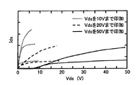
しかしながら、従来の窒化物半導体HEMTでは高いドレイン電圧を印加すると、ドレイン電流が減少してしまう現象(コラプス現象)が問題となっている。以下にコラプス現象につき説明する。図1は窒化物半導体HEMT(従来例)にドレイン電圧として順次10V、20V、50Vを印加したときのドレイン電流(Ids)−ドレイン電圧(Vds)特性を示している。ドレイン電圧を20V印加したときのドレイン電流は、ドレイン電圧を10V印加したときのドレイン電流に比べ減少する。さらに、ドレイン電圧を50V印加したときのドレイン電流は、ドレイン電圧10V印加したときのドレイン電流の約半分となっている。このようなHEMTにおいては、ドレイン電圧を20V以上印加することができず、高出力動作は難しい。 However, the conventional nitride semiconductor HEMT has a problem that a drain current decreases (collapse phenomenon) when a high drain voltage is applied. The collapse phenomenon will be described below. FIG. 1 shows drain current (Ids) -drain voltage (Vds) characteristics when 10 V, 20 V, and 50 V are sequentially applied to the nitride semiconductor HEMT (conventional example) as drain voltages. The drain current when a drain voltage of 20 V is applied is smaller than the drain current when a drain voltage of 10 V is applied. Furthermore, the drain current when a drain voltage of 50 V is applied is about half of the drain current when a drain voltage of 10 V is applied. In such a HEMT, a drain voltage of 20 V or higher cannot be applied, and high output operation is difficult.
本発明の目的は、高ドレイン電圧を印加したときに生じるコラプス現象を抑制し、高出力動作可能な窒化物半導体HEMTおよびその製造方法を提供することである。 An object of the present invention is to provide a nitride semiconductor HEMT that can suppress a collapse phenomenon that occurs when a high drain voltage is applied and can operate at a high output, and a method for manufacturing the same.
本発明は、基板上に順に形成されたGaN電子走行層、AlGaN電子供給層およびGaNキャップ層と、前記GaNキャップ層上に形成されたゲート電極と、該ゲート電極を挟んで形成されたソース電極およびドレイン電極と、前記ソース電極と前記ゲート電極との間および前記ゲート電極と前記ドレイン電極との間の前記GaNキャップ層の表面の全体に形成され、珪素の組成比が窒素に対し0.85〜1.12の窒化珪素からなる絶縁膜と、を具備することを特徴とする窒化物半導体HEMTである。本発明によれば、コラプス現象の原因となるゲート電極とドレイン電極の間の半導体表面層内に形成されるIII族元素の酸化物を減らすことができる。これによりコラプス現象を抑制することができる。よって、高出力動作可能な窒化物半導体HEMTを提供することが可能となる。 The present invention relates to a GaN electron transit layer, an AlGaN electron supply layer and a GaN cap layer formed in order on a substrate, a gate electrode formed on the GaN cap layer, and a source electrode formed with the gate electrode interposed therebetween. And the drain electrode, the source electrode and the gate electrode, and the entire surface of the GaN cap layer between the gate electrode and the drain electrode. The composition ratio of silicon is 0.85 with respect to nitrogen. a nitride semiconductor HEMT, characterized by comprising an insulating film made of silicon nitride of ~ 1.12, and. According to the present invention, group III element oxides formed in the semiconductor surface layer between the gate electrode and the drain electrode, which cause the collapse phenomenon, can be reduced. Thereby, the collapse phenomenon can be suppressed. Therefore, it is possible to provide a nitride semiconductor HEMT capable of high output operation.
本発明は前記基板は、SiC、Si、サファイアおよびGaN系半導体のいずれかからなることを特徴とする窒化物半導体HEMTとすることができる。 In the present invention, the substrate may be a nitride semiconductor HEMT , wherein the substrate is made of any one of SiC, Si, sapphire, and a GaN-based semiconductor .
本発明は、基板上にGaN電子走行層、AlGaN電子供給層およびGaNキャップ層を順に形成する工程と、前記GaNキャップ層の表面にプラズマCVD法によって、珪素の組成比が窒素に対し0.85〜1.12の窒化珪素からなる絶縁膜を形成する工程と、前記GaNキャップ層上にゲート電極を形成する工程と、前記ゲート電極を挟んでソース電極およびドレイン電極を形成する工程と、を具備し、前記絶縁膜は、前記ソース電極と前記ゲート電極との間および前記ゲート電極と前記ドレイン電極との間の前記GaNキャップ層の表面の全体に形成されることを特徴とする窒化物半導体HEMTの製造方法である。本発明によれば、コラプス現象の原因となるゲート電極とドレイン電極の間の半導体表面層内に形成されるIII族元素の酸化物を減らすことができる。これによりコラプス現象を抑制することができる。よって、高出力動作可能な窒化物半導体HEMTの製造方法を提供することが可能となる。 The present invention provides a step of forming a GaN electron transit layer, an AlGaN electron supply layer, and a GaN cap layer in this order on a substrate, and a plasma CVD method on the surface of the GaN cap layer so that the silicon composition ratio is 0.85 relative to nitrogen. ~ 1.12 forming an insulating film made of silicon nitride, forming a gate electrode on the GaN cap layer, and forming a source electrode and a drain electrode across the gate electrode. and the insulating film, the formed on the entire surface of the GaN cap layer nitride semiconductor HEMT, wherein Rukoto between and between the gate electrode and the drain electrode of the source electrode and the gate electrode It is a manufacturing method. According to the present invention, group III element oxides formed in the semiconductor surface layer between the gate electrode and the drain electrode, which cause the collapse phenomenon, can be reduced. Thereby, the collapse phenomenon can be suppressed. Therefore, it is possible to provide a method for manufacturing a nitride semiconductor HEMT capable of high output operation.
本発明は、前記窒化珪素からなる絶縁膜は、SiH4ガスの流量が4〜15sccm、NH3ガスの流量が0〜8sccm、N2ガスの流量が20〜200sccmにより形成されることを特徴とずる窒化物半導体HEMTの製造方法とすることができる。さらに、本発明は、前記絶縁膜は10nm以上で形成されることを特徴とする窒化物半導体HEMTの製造方法とすることができる。さらに、本発明は、前記GaN電子走行層、前記AlGaN電子供給層および前記GaNキャップ層は、MOCVD法で形成されることを特徴とする窒化物半導体HEMTの製造方法とすることができる。 The nitride film according to the present invention is characterized in that the insulating film made of silicon nitride is formed with a flow rate of SiH4 gas of 4 to 15 sccm, a flow rate of NH3 gas of 0 to 8 sccm, and a flow rate of N2 gas of 20 to 200 sccm . It can be set as the manufacturing method of semiconductor HEMT . Furthermore, the present invention can be a method for manufacturing a nitride semiconductor HEMT , wherein the insulating film is formed with a thickness of 10 nm or more. Furthermore, the present invention can be a method for manufacturing a nitride semiconductor HEMT , wherein the GaN electron transit layer, the AlGaN electron supply layer, and the GaN cap layer are formed by MOCVD.
本発明によれば、半導体表面層上に形成された絶縁膜層が、半導体表面層内の絶縁膜層界面に形成されるIII族元素の酸化物を減らし、これにより、高ドレイン電圧を印加したときに生じるコラプス現象を抑制することができる。この結果、高出力動作可能な窒化物半導体HEMTおよびその製造方法を提供することが可能となる。 According to the present invention, the insulating film layer formed on the semiconductor surface layer reduces the group III element oxide formed at the insulating film layer interface in the semiconductor surface layer, thereby applying a high drain voltage. The collapse phenomenon that sometimes occurs can be suppressed. As a result, it is possible to provide a nitride semiconductor HEMT capable of high output operation and a manufacturing method thereof.
本発明者は、コラプス現象の原因について、以下のように推論した。図2はコラプス現象の原因につき説明するための従来例にかかるHEMTの断面模式図である。サファイア基板またはSiC基板11上に、GaN系半導体層13として、GaNチャネル層およびAlGaN電子供給層を含む半導体層10、半導体表面層12であるGaNキャップ層が形成されている。GaN系半導体層13の表面に絶縁膜20が形成されている。さらに、絶縁膜20の所定領域に開口部を設け、開口部にGaN系半導体層13上にゲート電極18が形成されている。さらに、ゲート電極18を挟んでソース電極14およびドレイン電極16が形成されている。
The inventor inferred the cause of the collapse phenomenon as follows. FIG. 2 is a schematic sectional view of a HEMT according to a conventional example for explaining the cause of the collapse phenomenon. On the sapphire substrate or the SiC substrate 11, as the GaN-based
このとき、半導体表面層12内の絶縁膜層20界面には半導体表面層12を構成するIII族元素の酸化物40が存在する。ドレイン電流である電子46の流れ44は、ソース電極14からドレイン電極16に流れる。高ドレイン電圧を印加することにより、何らかの原因で、電子46の一部が、ゲート電極18とドレイン電極間の酸化物40に捕獲される。これにより、ドレイン電流が減少する。ここで、高電界によって、電子が捕獲されるメカニズムは明確ではないが、例えば、高ドレイン電圧印加時の高電界により酸化物40内に電子トラップ42が誘発する。または、高電界によって、ホットになった電子が表面空乏層を通過し、酸化物40内の電子トラップ42に捕獲される、などが考えられる。いずれにしても、コラプス現象は半導体表面層12内の絶縁膜層20界面に存在する酸化物40に起因するのではないかと推論した。そこで、本発明者は、半導体表面層内のIII族元素の酸化物を減らす手段として、標準生成自由エネルギーに着目した。
At this time, a Group III
ガリウム(Ga)、アルミニウム(Al)、インジウム(In)、珪素(Si)の酸化物における標準生成自由エネルギーは以下である。Ga2O3は−499kJ/mole、Al2O3は−791kJ/mole、In2O3は−419kJ/mole、SiO2は−857kJ/moleである。標準生成自由エネルギーとは反応の進み易さを表し、負に大きくなれば、自発的にその組成になるように反応が進むことを表す。 The standard free energy of formation in oxides of gallium (Ga), aluminum (Al), indium (In), and silicon (Si) is as follows. Ga 2 O 3 is −499 kJ / mole, Al 2 O 3 is −791 kJ / mole, In 2 O 3 is −419 kJ / mole, and SiO 2 is −857 kJ / mole. The standard free energy for generation indicates the easiness of the reaction, and if it becomes negative, it indicates that the reaction proceeds spontaneously so as to have the composition.
SiO2が標準生成自由エネルギーが最も小さい。半導体表面層12が例えばGaN層であった場合、その酸化物としてはGa2O3が考えられる。半導体表面層12であるGaN層は、窒素抜けによりGaが過剰な状態になる。そのため、大気中の酸素と反応し、例えばGa2O3のような酸化物が形成される。半導体表面層化学量論的な窒化珪素膜(Si3N4)より珪素(Si)の含有量の多い窒化珪素膜がGaN層上に形成されれば、窒化珪素膜中の余剰な珪素(余剰なボンドが水素と結合しSi−H基となっている珪素)は、GaN層内の酸化物であるGa2O3の酸素と反応し、珪素自らが酸化する。その結果、酸化物であるGa2O3を減らすことができると考えた。
SiO 2 has the smallest standard free energy of formation. When the
図3は、窒化珪素膜中の屈折率と、窒化珪素膜中の窒素に対する珪素の組成比(珪素/窒素組成比)との関係を示す図である。屈折率が2.0よりやや小さな値のとき、珪素と窒素は化学量論的な値である0.75となる。よって、屈折率が2.0以上であれば、窒化珪素膜中の珪素は化学量論的な窒化珪素膜より珪素が余剰になる。 Figure 3 is a diagram showing a refractive index in the silicon nitride film, the relationship between the composition ratio of silicon to nitrogen in the silicon nitride film (silicon / nitrogen composition ratio). When the refractive index is slightly smaller than 2.0, silicon and nitrogen have a stoichiometric value of 0.75. Therefore, if the refractive index is 2.0 or more, silicon in the silicon nitride film becomes more surplus than the stoichiometric silicon nitride film.
そこで、後述する実施例1と同じ構造を有する半導体装置において、絶縁膜層25として窒化珪素膜層の屈折率を2.05とした半導体装置と2.20とした半導体装置を作製した。
Therefore, in the semiconductor device having the same structure as that of Example 1 described later, a semiconductor device having a silicon nitride film layer having a refractive index of 2.05 and a semiconductor device having 2.20 as the insulating
表1は、絶縁膜層25として窒化珪素膜層の屈折率を2.05とした半導体装置と2.20とした半導体装置における、半導体表面層12と絶縁膜層25界面付近のエネルギー分散型蛍光X線分析(EDX分析)の結果である。半導体表面層12と絶縁膜層界面の絶縁膜層側の箇所30と半導体表面層側の箇所32の2箇所で分析を行っている。ここで、各元素の比率は組成比を示すものではなく、信号の強さを表している。
Table 1 shows energy dispersive fluorescence in the vicinity of the interface between the

屈折率2.05の窒化珪素膜層を有する半導体装置では、半導体表面層側の箇所32において、絶縁膜層側の箇所30に比べ、酸素とガリウムが多く検出される。これより、半導体表面層内にガリウム酸化物が形成されていることが考えられる。
In a semiconductor device having a silicon nitride film layer having a refractive index of 2.05, more oxygen and gallium are detected at the
一方、屈折率2.20の窒化珪素膜層を有する半導体装置では、屈折率2.05の窒化珪素膜層を有する半導体装置に比べ、半導体表面層側の箇所32の酸素が減っている。また、絶縁膜層側の箇所30の酸素が増えている。このことから、窒化珪素膜層の屈折率を2.20としたことにより、窒化珪素膜層中の余剰な珪素(すなわちSi−H基)が、半導体表面層内のガリウム酸化物中の酸素と反応し、その結果、ガリウム酸化物が減ったものと考えられる。
On the other hand, in a semiconductor device having a silicon nitride film layer with a refractive index of 2.20 , oxygen in the
このように、屈折率が2.2以上、すなわち珪素/窒素組成比が0.85以上の窒化珪素膜を半導体表面層12上に形成することにより、半導体表面層12内のIII族元素の酸化物を減ずることができる。ここで、屈折率が2.05でなく2.2以上が好ましいのは、ガリウム酸化物を減らすためにはある程度の余剰な珪素(Si−H基)が必要だからである。
Thus, by forming a silicon nitride film having a refractive index of 2.2 or more, that is, a silicon / nitrogen composition ratio of 0.85 or more on the
実施例1は、絶縁膜層25として屈折率2.2〜2.3、すなわち珪素/窒素組成比0.85〜0.9の窒化珪素膜層を半導体表面層12上に形成した窒化物半導体HEMTの例である。
Example 1 is a nitride semiconductor in which a silicon nitride film layer having a refractive index of 2.2 to 2.3, that is, a silicon / nitrogen composition ratio of 0.85 to 0.9 is formed on the
以下、窒化物半導体HEMTの製造方法について説明する。図4において、例えばSiC基板11上に、MOCVD法を用い、GaN系半導体層13として、不純物無添加のGaN電子走行層、Siを添加したN型のAlGaN電子供給層を含む半導体層10、半導体表面層12としてGaNキャップ層を形成する。これにより、エピタキシャル基板が完成する。半導体表面層12の表面に、絶縁膜層25として屈折率2.2〜2.3の窒化珪素膜層を形成する。この窒化珪素膜は、珪素/窒素組成比は0.85〜0.9に相当する。以上により、半導体製造用基板が完成する。基板11はSiC、Si、サファイアまたはGaN系半導体のいずれかからなる基板を用いることができる。これにより、結晶性のよいGaN系半導体層13を形成することができる。GaN系半導体13とは、例えば、GaN、AlGaN、InGaNのいずれかからなる半導体である。実施例1においては、GaN系半導体層13はGaN層およびAlGaN層からなる。
Hereinafter, a method for manufacturing the nitride semiconductor HEMT will be described. In FIG. 4, for example, on a SiC substrate 11, a MOCVD method is used, and as a GaN-based
絶縁膜層25である窒化珪素膜の形成は、プラズマCVD装置を用い、例えば、SiH4(シラン)ガスの流量を4.0〜15sccm、NH3(アンモニア)ガスの流量を0〜8%sccm、N2(窒素)ガスの流量を20〜200sccm、高周波電力密度を0.04〜0.24W/cm2の条件で行った。ここで、例えば、NH3ガスを低流量にすることで、珪素の含有量および屈折率を大きくすることができ、高周波電力密度を所定の値とすることで、珪素の含有量および所望の屈折率とすることができる。本実施例では、屈折率は2.2〜2.3、珪素/窒素組成比は0.85〜0.9とした。プラズマCVD装置としては平行平板型プラズマCVD装置、ICP型CVD装置、ECR型CVD装置を用いることができる。また、絶縁膜層25は、スパッタ装置を用い、例えば、Arのガス流量比を20〜80%、高周波電力を50〜500Wの条件で形成することもできる。絶縁膜層25の形成をCVD装置またはスパッタ装置を用いることにより、簡単に所望の絶縁膜層25を成膜することができる。
The silicon nitride film as the insulating
絶縁膜層25の膜厚は200nmから300nmを使用した。半導体表面層12表面の酸化物を減らす効果を得るためには、絶縁膜層25の膜厚は、10nm以上であることが好ましい。
The film thickness of the insulating
次に、図5において、所定領域の絶縁膜層25をドライエッチング法で選択的にエッチングし、半導体表面層12上にゲート電極16を形成する。ゲート電極18は、例えばNi/AlまたはNi/Auであり、蒸着法およびリフトオフ法により形成する。所定領域の絶縁膜層25をドライエッチング法で選択的にエッチングし、ゲート電極18を挟んでソース電極14およびドレイン電極16を形成する。ソース電極14およびドレイン電極16は、例えばTi/AlまたはTi/Auであり、蒸着法およびリフトオフ法により形成される。以上により、実施例1に係る窒化物半導体HEMTが完成する。
Next, in FIG. 5, the insulating
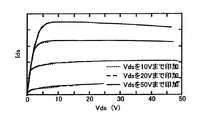
図6は、このように作製されたHEMTに、ドレイン電圧として順次10V、20V、50Vを印加したときのドレイン電流(Ids)−ドレイン電圧(Vds)特性を示している。いずれのドレイン電圧印加時も、ドレイン電流曲線はほぼ一致し、コラプス現象は生じていない。 FIG. 6 shows drain current (Ids) -drain voltage (Vds) characteristics when 10 V, 20 V, and 50 V are sequentially applied as drain voltages to the HEMT fabricated as described above. At any drain voltage application, the drain current curves are almost the same, and the collapse phenomenon does not occur.
このように、実施例1に係る窒化物半導体HEMTにおいては、絶縁膜層25として化学量論的な組成より珪素の多い窒化珪素膜層を、ゲート電極18とドレイン電極16間の半導体表面層12上に形成することにより、半導体表面層12内のIII族元素の酸化物を減ずることができた。これにより、コラプス現象を抑制させることができた。この結果、実施例1に係るHEMTにおいては、高出力動作可能な半導体装置の提供が可能となった。なお、実施例1においては、窒化物半導体HEMTの例を示したが、MESFET(Metal Semiconductor FET)においても同様の効果が得られる。
As described above, in the nitride semiconductor HEMT according to the first embodiment, the silicon nitride film layer containing more silicon than the stoichiometric composition is used as the insulating
また、図4に示した半導体装置製造用基板においては、絶縁膜層25がエピタキシャル基板の表面保護として機能する。基板上に種々の半導体層を形成したエピタキシャル基板は、予め作りだめをしておき、製造の所要があった場合に残りの工程を行う。あるいは、エピタキシャル成長技術を持たないメーカが、外部から購入して使用することになるものである。以上のように、エピタキシャル基板は、その表面が長期にわたって外部雰囲気に曝されることになるが、その間、表面の酸化などが進行してしまう。このようなエピタキシャル基板の表面に絶縁膜層25を形成しておくことにより、長期に外部雰囲気に曝されることがなくなる。その結果、GaN系半導体層13の表面に半導体装置の特性を劣化させる酸化物が形成されることを防止できる。従来の化学量論的な組成の絶縁膜においては、酸化物を低減させる機能は存在しなかった。しかし、実施例1に係る半導体装置を製造するための半導体装置製造用基板においては、絶縁膜25を設けることで、半導体表面層12に形成された酸化物を低減できるのである。よって、GaN系半導体層13の表面に半導体装置の特性を劣化させる酸化物が形成されることを防止できる。
In the semiconductor device manufacturing substrate shown in FIG. 4, the insulating
本実施例において、絶縁膜層25として屈折率2.1から2.2の窒化珪素膜層を使用した例を示した。絶縁膜層25は、窒化珪素膜層の屈折率が大きい方、すなわち窒化珪素膜中に珪素の含有量は多い方が、半導体表面層12内に形成された酸化物を減らす効果は大きい。言い換えると、屈折率の大きく、すなわち、窒素に対する珪素の組成比が大きい絶縁膜の効果が大きいと言える。しかし、珪素/窒素組成比が、例えば、3.0を越えると、大気中の酸素と反応してしまうため、窒化珪素膜下の酸化物との反応が低減されてしまう。さらに、珪素/窒素組成比が3.0を越える場合には、バンドギャップが急激に減少し、金属としての性質を帯び絶縁膜とはならず、アモルファス珪素となる。このため、珪素/窒素組成比は3.0以下とすることが
好ましい。
In this embodiment, an example in which a silicon nitride film layer having a refractive index of 2.1 to 2.2 is used as the insulating
以上のように、窒化珪素膜の珪素/窒素組成比は(珪素の組成比が窒素に対し)、珪素の組成を化学量論的な組成より多くするため、0.85以上であることが好ましい。0.85より小さいと、例えばGa2O3を引き抜くためのSi−H基の密度が足りないため、コラプス現象を抑制する効果が低くなるためである。また、上記より、珪素/窒素組成比は3.0以下が好ましい。さらに、1.0〜3.0がより好ましい。 As described above, the silicon / nitrogen composition ratio of the silicon nitride film (the silicon composition ratio is relative to nitrogen) is preferably 0.85 or more in order to make the silicon composition larger than the stoichiometric composition. . If it is smaller than 0.85, for example, the density of Si—H groups for pulling out Ga 2 O 3 is insufficient, and the effect of suppressing the collapse phenomenon becomes low. From the above, the silicon / nitrogen composition ratio is preferably 3.0 or less. Furthermore, 1.0 to 3.0 is more preferable.
本実施例において、半導体表面層12としてGaN層である場合の例を示した。しかし、前述の標準生成自由エネルギーを考慮すれば、例えば、GaNとAlNの混晶であるAlGaN層であっても同様に考えることができる。AlGaN層の表面にはガリウム酸化物とアルミニウム酸化物が形成されている。アルミニウム酸化物であるAl2O3の標準生成自由エネルギーよりSiO2の標準生成自由エネルギーの方が小さい。よって、絶縁膜層25内の余剰な珪素は、Ga2O3およびAl2O3の酸素と反応し、これら酸化物を減らすことができる。
In this embodiment, an example in which the
上記のごとく、特許文献1のような、ゲート電極とドレイン電極の間の半導体表面12層がAlGaN層である構造、特許文献2のような、ゲート電極とドレイン電極の間の半導体表面層12がGaN層である構造、および特許文献3のような、ゲート電極とドレイン電極の間の半導体表面層12がAlGaN層とGaN層である構造に対しても、半導体表面層12上に絶縁膜層25として化学量論的な組成より珪素が多く含まれた窒化珪素膜層を形成することにより、半導体表面層12内のIII族元素の酸化物を減らし、コラプス現象を抑制できる。
As described above, a structure in which the
また、絶縁膜層25としては、窒化珪素膜層のみならず、珪素を含む酸化珪素膜や窒化酸化珪素膜であっても、珪素が化学量論的な組成より多い膜であれば、余剰な珪素が、Ga2O3およびAl2O3の酸素と反応し、これら酸化物を減らす効果がある。
Further, as the insulating
酸化珪素膜を用いる場合は、酸化珪素膜の珪素/酸素組成比は(珪素の組成比が酸素に対し)、珪素の組成を化学量論的な組成比である0.5より多くするため、0.6以上であることが必要である。0.6より小さいと、例えばGa2O3を引き抜くためのSi−H基の密度が足りないため、コラプス現象を抑制する効果が低くなるためである。また、珪素/酸素組成比が3.0を越えると、窒化珪素膜と同様、大気中の酸素と反応してしまう。また、金属的な性質を帯びたアモルファス珪素となってしまう。以上より、酸化珪素膜の珪素/酸素組成比は(珪素の組成比が酸素に対し)、0.6以上が好ましく、3.0以下が好ましい。さらに、1.0〜3.0がより好ましい。 In the case of using a silicon oxide film, the silicon / oxygen composition ratio of the silicon oxide film (the composition ratio of silicon with respect to oxygen) is set so that the composition of silicon is greater than the stoichiometric composition ratio of 0.5. It is necessary to be 0.6 or more. If it is smaller than 0.6, for example, the density of Si—H groups for extracting Ga 2 O 3 is insufficient, and the effect of suppressing the collapse phenomenon becomes low. Further, when the silicon / oxygen composition ratio exceeds 3.0, it reacts with oxygen in the atmosphere like the silicon nitride film. In addition, it becomes amorphous silicon having metallic properties. From the above, the silicon / oxygen composition ratio of the silicon oxide film (the composition ratio of silicon with respect to oxygen) is preferably 0.6 or more, and more preferably 3.0 or less. Furthermore, 1.0 to 3.0 is more preferable.
酸化珪素膜の形成は、プラズマCVD装置を用い、例えば、SiH4ガスの流量を4〜10sccm、NO2(二酸化窒素)ガスの流量を2〜15sccm、N2ガスの流量を20〜500sccm、電力密度を0.03〜0.3W/cm2の条件で行うことができる。 The silicon oxide film is formed by using a plasma CVD apparatus. For example, the flow rate of SiH 4 gas is 4 to 10 sccm, the flow rate of NO 2 (nitrogen dioxide) gas is 2 to 15 sccm, the flow rate of N 2 gas is 20 to 500 sccm, power The density can be performed under the condition of 0.03 to 0.3 W / cm 2 .
酸化窒化珪素膜を用いる場合は、酸化窒化珪素膜の珪素/窒素並びに酸素組成比が(珪素の組成比が窒素および酸素に対し)0.6以上であることが必要である。0.6より小さいと、例えばGa2O3を引き抜くためのSi−H基の密度が足りないため、コラプス現象を抑制する効果が低くなるためである。また、珪素/窒素並びに酸素組成比が3.0を越えると、窒化珪素膜と同様、大気中の酸素と反応してしまう。また、金属的な性質を帯びたアモルファス珪素となってしまう。以上より、窒化酸化珪素膜の珪素/酸素および窒素組成比は(珪素の組成比が酸素および窒素に対し)、0.6以上が好ましく、3.0以下が好ましい。さらに、1.0〜3.0がより好ましい。 In the case of using a silicon oxynitride film, the silicon / nitrogen and oxygen composition ratio of the silicon oxynitride film (the composition ratio of silicon with respect to nitrogen and oxygen) needs to be 0.6 or more. If it is smaller than 0.6, for example, the density of Si—H groups for extracting Ga 2 O 3 is insufficient, and the effect of suppressing the collapse phenomenon becomes low. In addition, when the silicon / nitrogen and oxygen composition ratio exceeds 3.0, it reacts with oxygen in the atmosphere, like the silicon nitride film. In addition, it becomes amorphous silicon having metallic properties. From the above, the silicon / oxygen and nitrogen composition ratio of the silicon nitride oxide film (the silicon composition ratio with respect to oxygen and nitrogen) is preferably 0.6 or more, and more preferably 3.0 or less. Furthermore, 1.0 to 3.0 is more preferable.
酸化窒化珪素膜の形成は、平行平板型プラズマCVD装置を用い、例えば、SiH4ガスの流量を4〜10sccm、NO2(二酸化窒素)ガスの流量を2〜8sccm、N2ガスの流量を20〜500sccm、高周波電力密度を0.07〜0.25W/cm2の条件で行うことができる。 The silicon oxynitride film is formed using a parallel plate plasma CVD apparatus, for example, a flow rate of SiH 4 gas is 4 to 10 sccm, a flow rate of NO 2 (nitrogen dioxide) gas is 2 to 8 sccm, and a flow rate of N 2 gas is 20 It can be performed under the conditions of ˜500 sccm and high frequency power density of 0.07 to 0.25 W / cm 2 .
さらに、半導体表面層12としてGaN層の表面に形成されたGa2O3に対しては、絶縁膜層25としてアルミニウムが化学量論的な組成より多く含まれる窒化アルミニウム膜層や酸化アルミニウム膜層を使用することもできる。Al2O3の標準生成自由エネルギーはGa2O3の標準生成自由エネルギーに対し小さいため、絶縁膜層25中の余剰なアルミニウムがGa2O3の酸素と反応し、これら酸化物を減らす効果があるためである。
Furthermore, with respect to Ga 2 O 3 formed on the surface of the GaN layer as the
窒化アルミニウム膜を用いる場合は、窒化アルミニウム膜のアルミニウム/窒素組成比を化学量論的な組成である1.0より多くするため、1.2以上であることが必要である。1.2より小さいと、例えばGa2O3を引き抜くAlのダングリングボンドの密度が足りないため、コラプス現象を抑制する効果が低くなるためである。また、アルミニウム/窒素組成比が2.0を越えると、大気中の酸素と反応してしまうため、窒化アルミニウム膜下の酸化物との反応が低減されてしまう。以上より、窒化アルミニウム膜のアルミニウム/窒素組成比は(アルミニウムの組成比が窒素に対し)、1.2以上が好ましく
、2.0以下が好ましい。さらに、1.5〜2.0がより好ましい。
In the case of using an aluminum nitride film, the aluminum / nitrogen composition ratio of the aluminum nitride film needs to be 1.2 or more in order to increase the stoichiometric composition of 1.0. If the ratio is smaller than 1.2, for example, the dangling bond density of Al that pulls out Ga 2 O 3 is insufficient, and the effect of suppressing the collapse phenomenon becomes low. Further, when the aluminum / nitrogen composition ratio exceeds 2.0, it reacts with oxygen in the atmosphere, so that the reaction with the oxide under the aluminum nitride film is reduced. From the above, the aluminum / nitrogen composition ratio of the aluminum nitride film (the composition ratio of aluminum with respect to nitrogen) is preferably 1.2 or more, and more preferably 2.0 or less. Furthermore, 1.5 to 2.0 is more preferable.
窒化アルミニウム膜の形成は、窒化アルミニウム膜からなるターゲット、スパッタ法を用い、例えば、Arガスの流量が20〜100sccm、高周波電力が100〜200Wの条件で行うことができる。 The aluminum nitride film can be formed using a target made of an aluminum nitride film and a sputtering method, for example, under the conditions of an Ar gas flow rate of 20 to 100 sccm and a high-frequency power of 100 to 200 W.
酸化アルミニウム膜を用いる場合は、酸化アルミニウムのアルミニウム/酸素組成比は(アルミニウムの組成比が酸素に対し)、化学量論的な組成である0.67より多くするため、0.7以上であることが必要である。0.7より小さいと、例えばGa2O3を引き抜くAlのダングリングボンドの密度が足りないため、コラプス現象を抑制する効果が低くなるためである。また、アルミニウム/酸素組成比が2.0を越えると、大気中の酸素と反応してしまうため、窒化アルミニウム膜下の酸化物との反応が低減されてしまう。以上より、窒化アルミニウム膜のアルミニウム/窒素組成比は(アルミニウムの組成比が酸素に対し)、0.7以上が好ましく、2.0以下が好ましい。さらに、1.5〜2.0がより好ましい。 When an aluminum oxide film is used, the aluminum / oxygen composition ratio of aluminum oxide (the composition ratio of aluminum with respect to oxygen) is more than 0.7 because it is higher than the stoichiometric composition of 0.67. It is necessary. If it is smaller than 0.7, for example, the density of dangling bonds of Al that pulls out Ga 2 O 3 is insufficient, and the effect of suppressing the collapse phenomenon becomes low. Further, when the aluminum / oxygen composition ratio exceeds 2.0, it reacts with oxygen in the atmosphere, so that the reaction with the oxide under the aluminum nitride film is reduced. From the above, the aluminum / nitrogen composition ratio of the aluminum nitride film (the composition ratio of aluminum with respect to oxygen) is preferably 0.7 or more, and more preferably 2.0 or less. Furthermore, 1.5 to 2.0 is more preferable.
酸化アルミニウム膜の形成は、酸化アルミニウムからなるターゲット、スパッタ法を用い、例えば、Arガスの流量20〜100sccm、高周波電力100〜200Wの条件で行うことができる。 The aluminum oxide film can be formed using a target made of aluminum oxide and a sputtering method, for example, under conditions of Ar gas flow rate of 20 to 100 sccm and high frequency power of 100 to 200 W.
また、In2O3の標準生成自由エネルギーはAl2O3およびSiO2に対し大きいため。絶縁膜層25が珪素またはアルミニウムを化学量論的な組成より余剰に含む膜であれば、半導体表面層12として、GaN層の代わりにInGaN層であっても、インジウムの酸化物を減らす効果が得られる。
In addition, the standard free energy of formation of In 2 O 3 is larger than that of Al 2 O 3 and SiO 2 . If the insulating
以上説明したように、半導体表面層12上に形成された絶縁膜層25が以下の要件を満たせば、半導体表面層12内に形成されるIII族元素の酸化物を減らすことができる。この結果、コラプス現象を抑制でき、高出力動作可能な窒化物半導体HEMTあるいはMESFETを提供することができる。
As described above, the group III element oxide formed in the
ここで、前述の絶縁膜層25の要件としては、絶縁膜層25を構成する金属元素の酸化物の標準生成自由エネルギーをG1、半導体表面層12を構成するIII族元素の酸化物の標準生成自由エネルギーをG2としたとき、G1<G2であって、かつ化学量論的な組成より前記金属元素を多く含む絶縁膜層であることである。
Here, as the requirements for the insulating
10 半導体層
11 基板
12 半導体表面層
13 GaN系半導体層
14 ソース電極
16 ドレイン電極
18 ゲート電極
25 絶縁膜層
DESCRIPTION OF
Claims (6)
前記GaNキャップ層上に形成されたゲート電極と、該ゲート電極を挟んで形成されたソース電極およびドレイン電極と、
前記ソース電極と前記ゲート電極との間および前記ゲート電極と前記ドレイン電極との間の前記GaNキャップ層の表面の全体に形成され、珪素の組成比が窒素に対し0.85〜1.12の窒化珪素からなる絶縁膜と、
を具備することを特徴とする窒化物半導体HEMT。 A GaN electron transit layer, an AlGaN electron supply layer, and a GaN cap layer sequentially formed on the substrate;
A gate electrode formed on the GaN cap layer, a source electrode and a drain electrode formed across the gate electrode,
It is formed on the entire surface of the GaN cap layer between the source electrode and the gate electrode and between the gate electrode and the drain electrode, and the composition ratio of silicon is 0.85 to 1.12 . An insulating film made of silicon nitride ;
A nitride semiconductor HEMT , comprising:
前記GaNキャップ層の表面にプラズマCVD法によって、珪素の組成比が窒素に対し0.85〜1.12の窒化珪素からなる絶縁膜を形成する工程と、
前記GaNキャップ層上にゲート電極を形成する工程と、
前記ゲート電極を挟んでソース電極およびドレイン電極を形成する工程と、を具備し、
前記絶縁膜は、前記ソース電極と前記ゲート電極との間および前記ゲート電極と前記ドレイン電極との間の前記GaNキャップ層の表面の全体に形成されることを特徴とする窒化物半導体HEMTの製造方法。 Forming a GaN electron transit layer, an AlGaN electron supply layer, and a GaN cap layer in order on the substrate;
Forming an insulating film made of silicon nitride having a silicon composition ratio of 0.85 to 1.12 with respect to nitrogen by a plasma CVD method on the surface of the GaN cap layer;
Forming a gate electrode on the GaN cap layer;
Forming a source electrode and a drain electrode across the gate electrode , and
The insulating layer, the production of formed on the entire nitride semiconductor HEMT, wherein Rukoto surface of the GaN cap layer and between the said gate electrode and said drain electrode and said source electrode and said gate electrode Method.
Priority Applications (3)
| Application Number | Priority Date | Filing Date | Title |
|---|---|---|---|
| JP2005096902A JP4912604B2 (en) | 2005-03-30 | 2005-03-30 | Nitride semiconductor HEMT and manufacturing method thereof. |
| EP06251792.5A EP1708259B8 (en) | 2005-03-30 | 2006-03-30 | Semiconductor device having GaN-based semiconductor layer |
| US11/392,785 US8178900B2 (en) | 2005-03-30 | 2006-03-30 | Semiconductor device having GaN-based semiconductor layer and select composition ratio insulating film |
Applications Claiming Priority (1)
| Application Number | Priority Date | Filing Date | Title |
|---|---|---|---|
| JP2005096902A JP4912604B2 (en) | 2005-03-30 | 2005-03-30 | Nitride semiconductor HEMT and manufacturing method thereof. |
Publications (3)
| Publication Number | Publication Date |
|---|---|
| JP2006278812A JP2006278812A (en) | 2006-10-12 |
| JP2006278812A5 JP2006278812A5 (en) | 2008-04-24 |
| JP4912604B2 true JP4912604B2 (en) | 2012-04-11 |
Family
ID=36644868
Family Applications (1)
| Application Number | Title | Priority Date | Filing Date |
|---|---|---|---|
| JP2005096902A Active JP4912604B2 (en) | 2005-03-30 | 2005-03-30 | Nitride semiconductor HEMT and manufacturing method thereof. |
Country Status (3)
| Country | Link |
|---|---|
| US (1) | US8178900B2 (en) |
| EP (1) | EP1708259B8 (en) |
| JP (1) | JP4912604B2 (en) |
Cited By (2)
| Publication number | Priority date | Publication date | Assignee | Title |
|---|---|---|---|---|
| US9893210B2 (en) | 2015-09-24 | 2018-02-13 | Mitsubishi Electric Corporation | Semiconductor device and method of manufacturing the same |
| JP7301465B2 (en) | 2019-03-10 | 2023-07-03 | ジヤトコ株式会社 | power transmission device |
Families Citing this family (54)
| Publication number | Priority date | Publication date | Assignee | Title |
|---|---|---|---|---|
| JP4897948B2 (en) | 2005-09-02 | 2012-03-14 | 古河電気工業株式会社 | Semiconductor element |
| WO2008035403A1 (en) * | 2006-09-20 | 2008-03-27 | Fujitsu Limited | Field-effect transistor |
| JP2008198691A (en) * | 2007-02-09 | 2008-08-28 | New Japan Radio Co Ltd | Nitride semiconductor device |
| US7939853B2 (en) * | 2007-03-20 | 2011-05-10 | Power Integrations, Inc. | Termination and contact structures for a high voltage GaN-based heterojunction transistor |
| US20090321787A1 (en) * | 2007-03-20 | 2009-12-31 | Velox Semiconductor Corporation | High voltage GaN-based heterojunction transistor structure and method of forming same |
| JP5420157B2 (en) * | 2007-06-08 | 2014-02-19 | 住友電工デバイス・イノベーション株式会社 | Manufacturing method of semiconductor device |
| JP4963455B2 (en) * | 2007-09-04 | 2012-06-27 | 国立大学法人北海道大学 | Method and apparatus for forming an insulating film on the surface of a semiconductor substrate |
| US7915643B2 (en) | 2007-09-17 | 2011-03-29 | Transphorm Inc. | Enhancement mode gallium nitride power devices |
| JP5069531B2 (en) * | 2007-09-28 | 2012-11-07 | 富士フイルム株式会社 | Method for forming silicon nitride film |
| US8093136B2 (en) * | 2007-12-28 | 2012-01-10 | Semiconductor Energy Laboratory Co., Ltd. | Method for manufacturing SOI substrate |
| JP5345328B2 (en) | 2008-02-22 | 2013-11-20 | 住友電工デバイス・イノベーション株式会社 | Manufacturing method of semiconductor device |
| JP2009239230A (en) * | 2008-03-28 | 2009-10-15 | Fujitsu Ltd | Semiconductor device and method of manufacturing the same |
| US8519438B2 (en) * | 2008-04-23 | 2013-08-27 | Transphorm Inc. | Enhancement mode III-N HEMTs |
| US8289065B2 (en) | 2008-09-23 | 2012-10-16 | Transphorm Inc. | Inductive load power switching circuits |
| US7898004B2 (en) | 2008-12-10 | 2011-03-01 | Transphorm Inc. | Semiconductor heterostructure diodes |
| US8742459B2 (en) | 2009-05-14 | 2014-06-03 | Transphorm Inc. | High voltage III-nitride semiconductor devices |
| US8390000B2 (en) | 2009-08-28 | 2013-03-05 | Transphorm Inc. | Semiconductor devices with field plates |
| US8389977B2 (en) | 2009-12-10 | 2013-03-05 | Transphorm Inc. | Reverse side engineered III-nitride devices |
| US8242510B2 (en) * | 2010-01-28 | 2012-08-14 | Intersil Americas Inc. | Monolithic integration of gallium nitride and silicon devices and circuits, structure and method |
| JP2011210780A (en) * | 2010-03-29 | 2011-10-20 | Oki Electric Industry Co Ltd | GaN-MIS TRANSISTOR, GaN-IGBT AND METHOD FOR MANUFACTURING THEM |
| US8742460B2 (en) | 2010-12-15 | 2014-06-03 | Transphorm Inc. | Transistors with isolation regions |
| US8643062B2 (en) | 2011-02-02 | 2014-02-04 | Transphorm Inc. | III-N device structures and methods |
| US8716141B2 (en) | 2011-03-04 | 2014-05-06 | Transphorm Inc. | Electrode configurations for semiconductor devices |
| US8772842B2 (en) | 2011-03-04 | 2014-07-08 | Transphorm, Inc. | Semiconductor diodes with low reverse bias currents |
| US8901604B2 (en) | 2011-09-06 | 2014-12-02 | Transphorm Inc. | Semiconductor devices with guard rings |
| US9257547B2 (en) | 2011-09-13 | 2016-02-09 | Transphorm Inc. | III-N device structures having a non-insulating substrate |
| US8598937B2 (en) | 2011-10-07 | 2013-12-03 | Transphorm Inc. | High power semiconductor electronic components with increased reliability |
| JP5306438B2 (en) * | 2011-11-14 | 2013-10-02 | シャープ株式会社 | Field effect transistor and manufacturing method thereof |
| US8633094B2 (en) | 2011-12-01 | 2014-01-21 | Power Integrations, Inc. | GaN high voltage HFET with passivation plus gate dielectric multilayer structure |
| US9165766B2 (en) | 2012-02-03 | 2015-10-20 | Transphorm Inc. | Buffer layer structures suited for III-nitride devices with foreign substrates |
| JP5957994B2 (en) * | 2012-03-16 | 2016-07-27 | 富士通株式会社 | Manufacturing method of semiconductor device |
| JP6025242B2 (en) | 2012-03-30 | 2016-11-16 | 住友電工デバイス・イノベーション株式会社 | Manufacturing method of semiconductor device |
| US9093366B2 (en) | 2012-04-09 | 2015-07-28 | Transphorm Inc. | N-polar III-nitride transistors |
| US9184275B2 (en) | 2012-06-27 | 2015-11-10 | Transphorm Inc. | Semiconductor devices with integrated hole collectors |
| JP2014029908A (en) * | 2012-07-31 | 2014-02-13 | Toyota Central R&D Labs Inc | Semiconductor device and semiconductor device manufacturing method |
| JP6145985B2 (en) * | 2012-10-09 | 2017-06-14 | 日亜化学工業株式会社 | Field effect transistor |
| JP6106908B2 (en) | 2012-12-21 | 2017-04-05 | 住友電工デバイス・イノベーション株式会社 | Manufacturing method of semiconductor device |
| JP6093190B2 (en) * | 2013-01-18 | 2017-03-08 | 住友電気工業株式会社 | MIS structure transistor and method of manufacturing MIS structure transistor |
| CN105164811B (en) | 2013-02-15 | 2018-08-31 | 创世舫电子有限公司 | Electrode of semiconductor devices and forming method thereof |
| US8928037B2 (en) | 2013-02-28 | 2015-01-06 | Power Integrations, Inc. | Heterostructure power transistor with AlSiN passivation layer |
| US9087718B2 (en) | 2013-03-13 | 2015-07-21 | Transphorm Inc. | Enhancement-mode III-nitride devices |
| US9245993B2 (en) | 2013-03-15 | 2016-01-26 | Transphorm Inc. | Carbon doping semiconductor devices |
| US9443938B2 (en) | 2013-07-19 | 2016-09-13 | Transphorm Inc. | III-nitride transistor including a p-type depleting layer |
| US9318593B2 (en) | 2014-07-21 | 2016-04-19 | Transphorm Inc. | Forming enhancement mode III-nitride devices |
| US9536966B2 (en) | 2014-12-16 | 2017-01-03 | Transphorm Inc. | Gate structures for III-N devices |
| US9536967B2 (en) | 2014-12-16 | 2017-01-03 | Transphorm Inc. | Recessed ohmic contacts in a III-N device |
| JP6627441B2 (en) * | 2015-11-11 | 2020-01-08 | 住友電気工業株式会社 | Semiconductor device |
| JP6107922B2 (en) * | 2015-11-30 | 2017-04-05 | 富士通株式会社 | Semiconductor device |
| WO2017123999A1 (en) | 2016-01-15 | 2017-07-20 | Transphorm Inc. | Enhancement mode iii-nitride devices having an al(1-x)sixo gate insulator |
| TWI762486B (en) | 2016-05-31 | 2022-05-01 | 美商創世舫科技有限公司 | Iii-nitride devices including a graded depleting layer |
| JP6640687B2 (en) * | 2016-09-09 | 2020-02-05 | 株式会社東芝 | Semiconductor device |
| JP6885710B2 (en) * | 2016-11-16 | 2021-06-16 | 株式会社アドバンテスト | Compound semiconductor device and its manufacturing method |
| US10741494B2 (en) * | 2018-11-07 | 2020-08-11 | Semiconductor Components Industries, Llc | Electronic device including a contact structure contacting a layer |
| CN112382662B (en) * | 2020-11-13 | 2022-06-21 | 宁波铼微半导体有限公司 | Gallium nitride enhancement mode device and method of making same |
Family Cites Families (12)
| Publication number | Priority date | Publication date | Assignee | Title |
|---|---|---|---|---|
| JPH07211713A (en) * | 1994-01-17 | 1995-08-11 | Sumitomo Electric Ind Ltd | Annealing protective film |
| US6316820B1 (en) * | 1997-07-25 | 2001-11-13 | Hughes Electronics Corporation | Passivation layer and process for semiconductor devices |
| JPH11233731A (en) * | 1998-02-12 | 1999-08-27 | Mitsubishi Electric Corp | Schottky gate fet and monolithic type microwave integrated circuit device and its manufacture |
| JP2001077353A (en) | 1999-06-30 | 2001-03-23 | Toshiba Corp | High electron mobility transistor and power amplifier |
| JP4117535B2 (en) | 2001-11-30 | 2008-07-16 | 信越半導体株式会社 | Compound semiconductor device |
| JP4385205B2 (en) * | 2002-12-16 | 2009-12-16 | 日本電気株式会社 | Field effect transistor |
| JP4385206B2 (en) * | 2003-01-07 | 2009-12-16 | 日本電気株式会社 | Field effect transistor |
| JP4179539B2 (en) * | 2003-01-15 | 2008-11-12 | 富士通株式会社 | Compound semiconductor device and manufacturing method thereof |
| JP4077731B2 (en) * | 2003-01-27 | 2008-04-23 | 富士通株式会社 | Compound semiconductor device and manufacturing method thereof |
| JP4509031B2 (en) * | 2003-09-05 | 2010-07-21 | サンケン電気株式会社 | Nitride semiconductor device |
| US7045404B2 (en) * | 2004-01-16 | 2006-05-16 | Cree, Inc. | Nitride-based transistors with a protective layer and a low-damage recess and methods of fabrication thereof |
| JP2005286135A (en) * | 2004-03-30 | 2005-10-13 | Eudyna Devices Inc | Semiconductor device and manufacturing method thereof |
-
2005
- 2005-03-30 JP JP2005096902A patent/JP4912604B2/en active Active
-
2006
- 2006-03-30 EP EP06251792.5A patent/EP1708259B8/en active Active
- 2006-03-30 US US11/392,785 patent/US8178900B2/en active Active
Cited By (3)
| Publication number | Priority date | Publication date | Assignee | Title |
|---|---|---|---|---|
| US9893210B2 (en) | 2015-09-24 | 2018-02-13 | Mitsubishi Electric Corporation | Semiconductor device and method of manufacturing the same |
| DE102016217862B4 (en) | 2015-09-24 | 2022-09-01 | Mitsubishi Electric Corporation | Semiconductor device and method for manufacturing a semiconductor device |
| JP7301465B2 (en) | 2019-03-10 | 2023-07-03 | ジヤトコ株式会社 | power transmission device |
Also Published As
| Publication number | Publication date |
|---|---|
| EP1708259B8 (en) | 2015-01-07 |
| JP2006278812A (en) | 2006-10-12 |
| US20060220063A1 (en) | 2006-10-05 |
| US8178900B2 (en) | 2012-05-15 |
| EP1708259B1 (en) | 2014-10-22 |
| EP1708259A3 (en) | 2008-05-28 |
| EP1708259A2 (en) | 2006-10-04 |
Similar Documents
| Publication | Publication Date | Title |
|---|---|---|
| JP4912604B2 (en) | Nitride semiconductor HEMT and manufacturing method thereof. | |
| JP5813279B2 (en) | Cap layer containing aluminum nitride for nitride-based transistors and method of making the same | |
| EP2575180B1 (en) | Compound semiconductor device and method of manufacturing the same | |
| CN103715244B (en) | Semiconductor device and the manufacture method of semiconductor device | |
| JP6035007B2 (en) | MIS type nitride semiconductor HEMT and manufacturing method thereof | |
| JP5782947B2 (en) | Semiconductor device and manufacturing method thereof, power supply device, and high-frequency amplifier | |
| US9269782B2 (en) | Semiconductor device | |
| JP5724347B2 (en) | Compound semiconductor device and manufacturing method thereof | |
| JP5566670B2 (en) | GaN-based field effect transistor | |
| US20100127275A1 (en) | Gan-based field effect transistor and method of manufacturing the same | |
| JP5998446B2 (en) | Compound semiconductor device and manufacturing method thereof | |
| JPWO2008035403A1 (en) | Field effect transistor | |
| JP2007073555A (en) | Semiconductor element | |
| JP4134575B2 (en) | Semiconductor device and manufacturing method thereof | |
| JP5546104B2 (en) | GaN-based field effect transistor | |
| TW201314896A (en) | Compound semiconductor device and method for fabricating the same | |
| JP2010272728A (en) | GaN-BASED SEMICONDUCTOR ELEMENT AND METHOD OF MANUFACTURING THE SAME | |
| JP2007173426A (en) | Semiconductor device | |
| JP2009059946A (en) | Compound semiconductor device and method of manufacturing the same | |
| JP2005183733A (en) | High electron mobility transistor | |
| JP5101143B2 (en) | Field effect transistor and manufacturing method thereof | |
| JP2006286698A (en) | Electronic device and power converter | |
| JP6687831B2 (en) | Compound semiconductor device and manufacturing method thereof | |
| JP5605353B2 (en) | MIS type semiconductor device and manufacturing method thereof | |
| US9893210B2 (en) | Semiconductor device and method of manufacturing the same |
Legal Events
| Date | Code | Title | Description |
|---|---|---|---|
| A521 | Request for written amendment filed |
Free format text: JAPANESE INTERMEDIATE CODE: A523 Effective date: 20080310 |
|
| A621 | Written request for application examination |
Free format text: JAPANESE INTERMEDIATE CODE: A621 Effective date: 20080310 |
|
| A977 | Report on retrieval |
Free format text: JAPANESE INTERMEDIATE CODE: A971007 Effective date: 20110829 |
|
| A131 | Notification of reasons for refusal |
Free format text: JAPANESE INTERMEDIATE CODE: A131 Effective date: 20110906 |
|
| A521 | Request for written amendment filed |
Free format text: JAPANESE INTERMEDIATE CODE: A523 Effective date: 20111031 |
|
| TRDD | Decision of grant or rejection written | ||
| A01 | Written decision to grant a patent or to grant a registration (utility model) |
Free format text: JAPANESE INTERMEDIATE CODE: A01 Effective date: 20120117 |
|
| A01 | Written decision to grant a patent or to grant a registration (utility model) |
Free format text: JAPANESE INTERMEDIATE CODE: A01 |
|
| A61 | First payment of annual fees (during grant procedure) |
Free format text: JAPANESE INTERMEDIATE CODE: A61 Effective date: 20120118 |
|
| R150 | Certificate of patent or registration of utility model |
Free format text: JAPANESE INTERMEDIATE CODE: R150 Ref document number: 4912604 Country of ref document: JP Free format text: JAPANESE INTERMEDIATE CODE: R150 |
|
| FPAY | Renewal fee payment (event date is renewal date of database) |
Free format text: PAYMENT UNTIL: 20150127 Year of fee payment: 3 |
|
| R250 | Receipt of annual fees |
Free format text: JAPANESE INTERMEDIATE CODE: R250 |
|
| R250 | Receipt of annual fees |
Free format text: JAPANESE INTERMEDIATE CODE: R250 |