JP5160225B2 - Method for fabricating nitride-based transistor with regrowth ohmic contact region and nitride-based transistor with regrowth ohmic contact region - Google Patents
Method for fabricating nitride-based transistor with regrowth ohmic contact region and nitride-based transistor with regrowth ohmic contact region Download PDFInfo
- Publication number
- JP5160225B2 JP5160225B2 JP2007527194A JP2007527194A JP5160225B2 JP 5160225 B2 JP5160225 B2 JP 5160225B2 JP 2007527194 A JP2007527194 A JP 2007527194A JP 2007527194 A JP2007527194 A JP 2007527194A JP 5160225 B2 JP5160225 B2 JP 5160225B2
- Authority
- JP
- Japan
- Prior art keywords
- layer
- contact
- nitride
- providing
- channel layer
- Prior art date
- Legal status (The legal status is an assumption and is not a legal conclusion. Google has not performed a legal analysis and makes no representation as to the accuracy of the status listed.)
- Active
Links
- 150000004767 nitrides Chemical class 0.000 title claims description 108
- 238000000034 method Methods 0.000 title claims description 53
- 230000004888 barrier function Effects 0.000 claims description 97
- 239000000463 material Substances 0.000 claims description 71
- 238000004519 manufacturing process Methods 0.000 claims description 48
- 239000004065 semiconductor Substances 0.000 claims description 48
- 229910002704 AlGaN Inorganic materials 0.000 claims description 27
- 229910052751 metal Inorganic materials 0.000 claims description 26
- 239000002184 metal Substances 0.000 claims description 26
- 229910052581 Si3N4 Inorganic materials 0.000 claims description 14
- 238000000059 patterning Methods 0.000 claims description 14
- HQVNEWCFYHHQES-UHFFFAOYSA-N silicon nitride Chemical compound N12[Si]34N5[Si]62N3[Si]51N64 HQVNEWCFYHHQES-UHFFFAOYSA-N 0.000 claims description 14
- 238000000137 annealing Methods 0.000 claims description 11
- 238000000623 plasma-assisted chemical vapour deposition Methods 0.000 claims description 11
- 230000015572 biosynthetic process Effects 0.000 claims description 10
- 238000005137 deposition process Methods 0.000 claims description 10
- 229910052710 silicon Inorganic materials 0.000 claims description 10
- 238000002248 hydride vapour-phase epitaxy Methods 0.000 claims description 8
- 238000002161 passivation Methods 0.000 claims description 6
- 238000004544 sputter deposition Methods 0.000 claims description 6
- 238000001451 molecular beam epitaxy Methods 0.000 claims description 5
- 230000005533 two-dimensional electron gas Effects 0.000 claims description 5
- 238000005229 chemical vapour deposition Methods 0.000 claims description 4
- 229910001092 metal group alloy Inorganic materials 0.000 claims description 4
- 229920002120 photoresistant polymer Polymers 0.000 claims description 3
- 238000010894 electron beam technology Methods 0.000 claims description 2
- 229910002601 GaN Inorganic materials 0.000 description 31
- 238000010586 diagram Methods 0.000 description 20
- 239000000758 substrate Substances 0.000 description 20
- HBMJWWWQQXIZIP-UHFFFAOYSA-N silicon carbide Chemical compound [Si+]#[C-] HBMJWWWQQXIZIP-UHFFFAOYSA-N 0.000 description 14
- 238000000151 deposition Methods 0.000 description 13
- 229910010271 silicon carbide Inorganic materials 0.000 description 13
- 230000008021 deposition Effects 0.000 description 12
- 230000008569 process Effects 0.000 description 9
- 238000005530 etching Methods 0.000 description 7
- IJGRMHOSHXDMSA-UHFFFAOYSA-N Atomic nitrogen Chemical compound N#N IJGRMHOSHXDMSA-UHFFFAOYSA-N 0.000 description 6
- JMASRVWKEDWRBT-UHFFFAOYSA-N Gallium nitride Chemical compound [Ga]#N JMASRVWKEDWRBT-UHFFFAOYSA-N 0.000 description 6
- 238000001020 plasma etching Methods 0.000 description 6
- JBRZTFJDHDCESZ-UHFFFAOYSA-N AsGa Chemical compound [As]#[Ga] JBRZTFJDHDCESZ-UHFFFAOYSA-N 0.000 description 5
- RNQKDQAVIXDKAG-UHFFFAOYSA-N aluminum gallium Chemical compound [Al].[Ga] RNQKDQAVIXDKAG-UHFFFAOYSA-N 0.000 description 5
- 150000001875 compounds Chemical class 0.000 description 5
- 239000007943 implant Substances 0.000 description 5
- 230000007704 transition Effects 0.000 description 5
- -1 Al x Ga 1-x N Chemical class 0.000 description 4
- 229910001218 Gallium arsenide Inorganic materials 0.000 description 4
- XUIMIQQOPSSXEZ-UHFFFAOYSA-N Silicon Chemical compound [Si] XUIMIQQOPSSXEZ-UHFFFAOYSA-N 0.000 description 4
- 229910052782 aluminium Inorganic materials 0.000 description 4
- XAGFODPZIPBFFR-UHFFFAOYSA-N aluminium Chemical compound [Al] XAGFODPZIPBFFR-UHFFFAOYSA-N 0.000 description 4
- 239000010703 silicon Substances 0.000 description 4
- VYPSYNLAJGMNEJ-UHFFFAOYSA-N Silicium dioxide Chemical compound O=[Si]=O VYPSYNLAJGMNEJ-UHFFFAOYSA-N 0.000 description 3
- 230000015556 catabolic process Effects 0.000 description 3
- 239000013078 crystal Substances 0.000 description 3
- 239000002019 doping agent Substances 0.000 description 3
- 238000001312 dry etching Methods 0.000 description 3
- 238000002513 implantation Methods 0.000 description 3
- 229910052757 nitrogen Inorganic materials 0.000 description 3
- 230000006911 nucleation Effects 0.000 description 3
- 238000010899 nucleation Methods 0.000 description 3
- 229910052594 sapphire Inorganic materials 0.000 description 3
- 239000010980 sapphire Substances 0.000 description 3
- 238000001039 wet etching Methods 0.000 description 3
- PMHQVHHXPFUNSP-UHFFFAOYSA-M copper(1+);methylsulfanylmethane;bromide Chemical compound Br[Cu].CSC PMHQVHHXPFUNSP-UHFFFAOYSA-M 0.000 description 2
- 239000003989 dielectric material Substances 0.000 description 2
- 230000005669 field effect Effects 0.000 description 2
- 238000005468 ion implantation Methods 0.000 description 2
- 230000001788 irregular Effects 0.000 description 2
- 238000004518 low pressure chemical vapour deposition Methods 0.000 description 2
- GYHNNYVSQQEPJS-UHFFFAOYSA-N Gallium Chemical compound [Ga] GYHNNYVSQQEPJS-UHFFFAOYSA-N 0.000 description 1
- 238000009825 accumulation Methods 0.000 description 1
- 239000000969 carrier Substances 0.000 description 1
- 230000008859 change Effects 0.000 description 1
- 238000005520 cutting process Methods 0.000 description 1
- 230000003247 decreasing effect Effects 0.000 description 1
- 230000007547 defect Effects 0.000 description 1
- 238000000407 epitaxy Methods 0.000 description 1
- 238000011049 filling Methods 0.000 description 1
- 229910052733 gallium Inorganic materials 0.000 description 1
- 150000004678 hydrides Chemical class 0.000 description 1
- 239000012535 impurity Substances 0.000 description 1
- 229910052738 indium Inorganic materials 0.000 description 1
- APFVFJFRJDLVQX-UHFFFAOYSA-N indium atom Chemical compound [In] APFVFJFRJDLVQX-UHFFFAOYSA-N 0.000 description 1
- 238000002955 isolation Methods 0.000 description 1
- 238000001465 metallisation Methods 0.000 description 1
- 230000005012 migration Effects 0.000 description 1
- 238000013508 migration Methods 0.000 description 1
- 239000000203 mixture Substances 0.000 description 1
- 229910052759 nickel Inorganic materials 0.000 description 1
- TWNQGVIAIRXVLR-UHFFFAOYSA-N oxo(oxoalumanyloxy)alumane Chemical compound O=[Al]O[Al]=O TWNQGVIAIRXVLR-UHFFFAOYSA-N 0.000 description 1
- 229910052763 palladium Inorganic materials 0.000 description 1
- 230000003071 parasitic effect Effects 0.000 description 1
- 230000000737 periodic effect Effects 0.000 description 1
- 229910052697 platinum Inorganic materials 0.000 description 1
- 230000010287 polarization Effects 0.000 description 1
- 238000004886 process control Methods 0.000 description 1
- 230000009467 reduction Effects 0.000 description 1
- 230000008439 repair process Effects 0.000 description 1
- 229910021332 silicide Inorganic materials 0.000 description 1
- FVBUAEGBCNSCDD-UHFFFAOYSA-N silicide(4-) Chemical compound [Si-4] FVBUAEGBCNSCDD-UHFFFAOYSA-N 0.000 description 1
- 235000012239 silicon dioxide Nutrition 0.000 description 1
- 239000000377 silicon dioxide Substances 0.000 description 1
- LIVNPJMFVYWSIS-UHFFFAOYSA-N silicon monoxide Chemical compound [Si-]#[O+] LIVNPJMFVYWSIS-UHFFFAOYSA-N 0.000 description 1
- 229910052814 silicon oxide Inorganic materials 0.000 description 1
- 125000006850 spacer group Chemical group 0.000 description 1
- 238000000927 vapour-phase epitaxy Methods 0.000 description 1
Images


Classifications
-
- H—ELECTRICITY
- H01—ELECTRIC ELEMENTS
- H01L—SEMICONDUCTOR DEVICES NOT COVERED BY CLASS H10
- H01L29/00—Semiconductor devices specially adapted for rectifying, amplifying, oscillating or switching and having potential barriers; Capacitors or resistors having potential barriers, e.g. a PN-junction depletion layer or carrier concentration layer; Details of semiconductor bodies or of electrodes thereof ; Multistep manufacturing processes therefor
- H01L29/66—Types of semiconductor device ; Multistep manufacturing processes therefor
- H01L29/68—Types of semiconductor device ; Multistep manufacturing processes therefor controllable by only the electric current supplied, or only the electric potential applied, to an electrode which does not carry the current to be rectified, amplified or switched
- H01L29/76—Unipolar devices, e.g. field effect transistors
- H01L29/772—Field effect transistors
- H01L29/778—Field effect transistors with two-dimensional charge carrier gas channel, e.g. HEMT ; with two-dimensional charge-carrier layer formed at a heterojunction interface
- H01L29/7786—Field effect transistors with two-dimensional charge carrier gas channel, e.g. HEMT ; with two-dimensional charge-carrier layer formed at a heterojunction interface with direct single heterostructure, i.e. with wide bandgap layer formed on top of active layer, e.g. direct single heterostructure MIS-like HEMT
- H01L29/7787—Field effect transistors with two-dimensional charge carrier gas channel, e.g. HEMT ; with two-dimensional charge-carrier layer formed at a heterojunction interface with direct single heterostructure, i.e. with wide bandgap layer formed on top of active layer, e.g. direct single heterostructure MIS-like HEMT with wide bandgap charge-carrier supplying layer, e.g. direct single heterostructure MODFET
-
- H—ELECTRICITY
- H01—ELECTRIC ELEMENTS
- H01L—SEMICONDUCTOR DEVICES NOT COVERED BY CLASS H10
- H01L29/00—Semiconductor devices specially adapted for rectifying, amplifying, oscillating or switching and having potential barriers; Capacitors or resistors having potential barriers, e.g. a PN-junction depletion layer or carrier concentration layer; Details of semiconductor bodies or of electrodes thereof ; Multistep manufacturing processes therefor
- H01L29/66—Types of semiconductor device ; Multistep manufacturing processes therefor
- H01L29/66007—Multistep manufacturing processes
- H01L29/66075—Multistep manufacturing processes of devices having semiconductor bodies comprising group 14 or group 13/15 materials
- H01L29/66227—Multistep manufacturing processes of devices having semiconductor bodies comprising group 14 or group 13/15 materials the devices being controllable only by the electric current supplied or the electric potential applied, to an electrode which does not carry the current to be rectified, amplified or switched, e.g. three-terminal devices
- H01L29/66409—Unipolar field-effect transistors
- H01L29/66446—Unipolar field-effect transistors with an active layer made of a group 13/15 material, e.g. group 13/15 velocity modulation transistor [VMT], group 13/15 negative resistance FET [NERFET]
- H01L29/66454—Static induction transistors [SIT], e.g. permeable base transistors [PBT]
-
- H—ELECTRICITY
- H01—ELECTRIC ELEMENTS
- H01L—SEMICONDUCTOR DEVICES NOT COVERED BY CLASS H10
- H01L29/00—Semiconductor devices specially adapted for rectifying, amplifying, oscillating or switching and having potential barriers; Capacitors or resistors having potential barriers, e.g. a PN-junction depletion layer or carrier concentration layer; Details of semiconductor bodies or of electrodes thereof ; Multistep manufacturing processes therefor
- H01L29/66—Types of semiconductor device ; Multistep manufacturing processes therefor
- H01L29/68—Types of semiconductor device ; Multistep manufacturing processes therefor controllable by only the electric current supplied, or only the electric potential applied, to an electrode which does not carry the current to be rectified, amplified or switched
- H01L29/76—Unipolar devices, e.g. field effect transistors
- H01L29/772—Field effect transistors
- H01L29/778—Field effect transistors with two-dimensional charge carrier gas channel, e.g. HEMT ; with two-dimensional charge-carrier layer formed at a heterojunction interface
-
- H—ELECTRICITY
- H01—ELECTRIC ELEMENTS
- H01L—SEMICONDUCTOR DEVICES NOT COVERED BY CLASS H10
- H01L29/00—Semiconductor devices specially adapted for rectifying, amplifying, oscillating or switching and having potential barriers; Capacitors or resistors having potential barriers, e.g. a PN-junction depletion layer or carrier concentration layer; Details of semiconductor bodies or of electrodes thereof ; Multistep manufacturing processes therefor
- H01L29/02—Semiconductor bodies ; Multistep manufacturing processes therefor
- H01L29/12—Semiconductor bodies ; Multistep manufacturing processes therefor characterised by the materials of which they are formed
- H01L29/20—Semiconductor bodies ; Multistep manufacturing processes therefor characterised by the materials of which they are formed including, apart from doping materials or other impurities, only AIIIBV compounds
- H01L29/2003—Nitride compounds
Landscapes
- Engineering & Computer Science (AREA)
- Microelectronics & Electronic Packaging (AREA)
- Power Engineering (AREA)
- Physics & Mathematics (AREA)
- Ceramic Engineering (AREA)
- Condensed Matter Physics & Semiconductors (AREA)
- General Physics & Mathematics (AREA)
- Computer Hardware Design (AREA)
- Manufacturing & Machinery (AREA)
- Junction Field-Effect Transistors (AREA)
- Electrodes Of Semiconductors (AREA)
Description
本発明は、半導体デバイスに関し、より詳細には、窒化物をベースにした能動層を組み込んだトランジスタ及び高電子移動度トランジスタン並びにその製造方法に関する。 The present invention relates to semiconductor devices, and more particularly to a transistor incorporating a nitride-based active layer, a high electron mobility transistor, and a method for manufacturing the same.
本発明は、大電力、高温、及び/又は高周波用途に適したトランジスタを作ることができる半導体材料で形成されたトランジスタに関する。シリコン(Si)及びガリウム砒素(GaAs)のような材料は、低電力及び(Siの場合には)低周波用途の半導体デバイスに広く応用されている。しかし、これらの比較的よく知られている半導体材料は、比較的小さなバンドギャップ(例えば、室温において、Siで1.12eV及びGaAsで1.42eV)及び/又は比較的小さな破壊電圧のために、より高い電力及び/又は高周波数用途に十分に適していない可能性がある。 The present invention relates to a transistor formed of a semiconductor material capable of making a transistor suitable for high power, high temperature, and / or high frequency applications. Materials such as silicon (Si) and gallium arsenide (GaAs) are widely applied in low power and (in the case of Si) low frequency semiconductor devices. However, these relatively well-known semiconductor materials have a relatively small band gap (eg, 1.12 eV for Si and 1.42 eV for GaAs at room temperature) and / or a relatively small breakdown voltage. It may not be well suited for higher power and / or high frequency applications.
Si及びGaAsで起こる問題を考慮して、大電力、高温及び/又は高周波用途ならびにデバイスに対する関心は、炭化珪素(アルファSiCの場合に室温で2.996eV)及びIII族窒化物(例えば、GaNの場合に室温で3.36eV)のような広いバンドギャップの半導体材料に向いている。これらの材料は、一般に、ガリウム砒素及びシリコンに比べて、電界破壊強度がより高く、かつ電子飽和速度がより高い。 Considering the problems that occur with Si and GaAs, interest in high power, high temperature and / or high frequency applications and devices is of interest for silicon carbide (2.996 eV at room temperature for alpha SiC) and III-nitrides (eg GaN In some cases, it is suitable for a semiconductor material having a wide band gap such as 3.36 eV at room temperature. These materials generally have higher field breakdown strengths and higher electron saturation rates than gallium arsenide and silicon.
大電力及び/又は高周波用途で、特に関心のある半導体デバイスは、高電子移動度トランジスタ(HEMT)であり、この高電子移動度トランジスタは、変調ドープ電界効果トランジスタ(MODFET)としても知られている。異なるバンドギャップエネルギーを有しバンドギャップの小さい方の材料がより大きな電子親和力を有している2つの半導体材料のヘテロ接合に2次元電子ガス(2DEG)が形成され、この半導体デバイスは、いくつかの状況の下で動作上の有利点を示すことができる。2DEGは、アンドープ(「故意でなくドープされた」)でより小さなバンドギャップの材料の中の蓄積層であり、例えば、1013キャリア/cm2を超える非常に高いシート電子濃度を含むことができる。その上、より広いバンドギャップの半導体で生じる電子は、イオン化不純物散乱の減少のために高電子移動度を可能にする2DEGに移る。 A semiconductor device of particular interest for high power and / or high frequency applications is the high electron mobility transistor (HEMT), which is also known as a modulation doped field effect transistor (MODFET). . A two-dimensional electron gas (2DEG) is formed at the heterojunction of two semiconductor materials with different bandgap energies and the smaller bandgap material having a higher electron affinity. Operational advantages can be shown under the circumstances. 2DEG is an accumulation layer in an undoped (“unintentionally doped”), smaller bandgap material, and can include, for example, very high sheet electron concentrations exceeding 10 13 carriers / cm 2. . Moreover, electrons generated in wider bandgap semiconductors are transferred to 2DEG, which allows high electron mobility due to reduced ionized impurity scattering.
高いキャリア濃度と高いキャリア移動度のこの組合せは、HEMTに非常に大きな相互コンダクタンスを与えることができ、さらに、高周波用途に関して、金属半導体電界効果トランジスタ(MESFET)に優る大きな性能上の有利点を提供することができる。 This combination of high carrier concentration and high carrier mobility can give HEMT very large transconductance, and also provides significant performance advantages over metal semiconductor field effect transistors (MESFETs) for high frequency applications. can do.
窒化ガリウム/窒化アルミニウムガリウム(GaN/AlGaN)材料系で製作された高電子移動度トランジスタは、上述した高破壊電界、広いバンドギャップ、大きな伝導帯食い違い、及び/又は高い飽和電子ドリフト速度を含む材料特性の組合せのために、大量のRF電力を生成する可能性を有している。2DEGの電子の大部分は、AlGaNの分極によっている。GaN/AlGaN系のHEMTは、既に実証されている。AlGaN/GaNHEMT構造及びその製造方法が開示されている(例えば、特許文献1及び2参照)。半絶縁性炭化珪素基板、この基板の上の窒化アルミニウムバッファ層、このバッファ層の上の絶縁性窒化ガリウム層、この窒化ガリウム層の上の窒化アルミニウムガリウム層、及び窒化アルミニウムガリウム能動構造の上の不動態化層を有するHEMTデバイスが開示されている(例えば、sheppardらの特許文献3参照、この特許は一般的に譲渡されており、参照して本明細書に組み込まれる)。
A high electron mobility transistor fabricated in a gallium nitride / aluminum gallium nitride (GaN / AlGaN) material system is a material that includes the high breakdown field, wide band gap, large conduction band gap, and / or high saturation electron drift velocity described above. Because of the combination of properties, it has the potential to generate large amounts of RF power. Most of the electrons of 2DEG are due to the polarization of AlGaN. GaN / AlGaN-based HEMTs have already been demonstrated. An AlGaN / GaN HEMT structure and a manufacturing method thereof are disclosed (for example, see
窒化物ベースのトランジスタの製作に関する1つの問題は、そのようなトランジスタのオーミックコンタクト(ohmic contact)の形成に関係している。従来、オーミックコンタクトは、コンタクト用の凹部を反応性イオンエッチング(RIE)することによって形成された。しかし、厳密なプロセス制御の実行がなければ、窒化物ベースの材料のRIEには、不均一性及び再現性の問題が欠点としてある可能性がある。そのような問題は、製作プロセスを制御することの難しさに帰着することができる。RIEなしで形成されるオーミックコンタクトでは、一般に、高いアニール温度(例えば、900℃)が使用されてきた。そのような高いアニール温度は、材料及び/又はデバイスに損傷を与える可能性がある。 One problem with the fabrication of nitride based transistors is related to the formation of ohmic contacts for such transistors. Conventionally, an ohmic contact is formed by reactive ion etching (RIE) of a recess for contact. However, without strict process control execution, RIE of nitride-based materials can suffer from non-uniformity and reproducibility problems. Such problems can result in difficulties in controlling the fabrication process. For ohmic contacts formed without RIE, high annealing temperatures (eg, 900 ° C.) have generally been used. Such high annealing temperatures can damage materials and / or devices.
本発明は、このような問題に鑑みてなされたもので、その目的とするところは、窒化物をベースにした能動層を組み込んだトランジスタ及び高電子移動度トランジスタ並びにその製造方法を提供することにある。 The present invention has been made in view of such problems, and an object of the present invention is to provide a transistor incorporating a nitride-based active layer, a high electron mobility transistor, and a method for manufacturing the same. is there.
本発明のいくつかの実施形態は、基板上に窒化物ベースのチャネル層を形成すること、窒化物ベースのチャネル層上に障壁層を形成すること、窒化物ベースのチャネル層のコンタクト領域を露出させるように障壁層にコンタクト凹部を形成すること、及び低温堆積プロセスを使用して窒化物ベースのチャネル層の露出されたコンタクト領域上にコンタクト層を形成することを含んだ、トランジスタの製作を可能にする。製作は、また、コンタクト層上にオーミックコンタクトを形成すること及びオーミックコンタクトに隣接した障壁層上に配置されたゲートコンタクトを形成すること、を含むことができる。 Some embodiments of the present invention include forming a nitride-based channel layer on a substrate, forming a barrier layer on the nitride-based channel layer, exposing a contact region of the nitride-based channel layer Allows the fabrication of transistors, including forming contact recesses in the barrier layer to form, and using a low temperature deposition process to form a contact layer over the exposed contact region of the nitride-based channel layer To. Fabrication can also include forming an ohmic contact on the contact layer and forming a gate contact disposed on the barrier layer adjacent to the ohmic contact.
本発明のさらに他の実施形態では、低温堆積プロセスを使用して窒化物ベースのチャネル層の露出されたコンタクト領域上にコンタクト層を形成することは、有機金属化学気相成長(MOCVD)、分子線エピタキシィ(MBE)、プラズマ増速化学気相成長(PECVD)、スパッタリング及び/又は水素化物気相エピタキシィ(HVPE)によって、コンタクト層を形成することを含んでいる。さらに、低温堆積プロセスは、トランジスタが形成されるウェーハからの質量の輸送以外のプロセスである可能性がある。 In yet another embodiment of the invention, forming the contact layer on the exposed contact region of the nitride-based channel layer using a low temperature deposition process comprises metal organic chemical vapor deposition (MOCVD), molecular Forming a contact layer by line epitaxy (MBE), plasma enhanced chemical vapor deposition (PECVD), sputtering and / or hydride vapor phase epitaxy (HVPE). Further, the low temperature deposition process may be a process other than mass transport from the wafer on which the transistor is formed.
本発明の追加の実施形態おいて、トランジスタの製作は、さらに、障壁層上に第1の誘電体層を形成すること、及び第1の誘電体層にゲート凹部を形成することを含んでいる。ゲートコンタクトを形成することは、このゲート凹部にゲートコンタクトを形成することを含んでいる。コンタクト凹部を形成することは、窒化物ベースのチャネル層の部分を露出させるコンタクト凹部を第1の誘電体層及び障壁層に形成することを含んでいる。本発明の他の実施形態では、ゲートコンタクトは、第1の誘電体層上に形成することができる。 In additional embodiments of the present invention, the fabrication of the transistor further includes forming a first dielectric layer on the barrier layer and forming a gate recess in the first dielectric layer. . Forming the gate contact includes forming a gate contact in the gate recess. Forming the contact recesses includes forming contact recesses in the first dielectric layer and the barrier layer that expose portions of the nitride-based channel layer. In other embodiments of the invention, the gate contact may be formed on the first dielectric layer.
本発明のさらに他の実施形態において、第1の誘電体層は、窒化珪素層を備えている。この窒化珪素層は、トランジスタの不動態化層を実現することができる。 In yet another embodiment of the present invention, the first dielectric layer comprises a silicon nitride layer. This silicon nitride layer can realize a passivation layer of the transistor.
本発明の追加の実施形態では、コンタクト凹部は、チャネル層の中まで延びる。さらに、オーミックコンタクトを形成することは、オーミックコンタクトをアニールすることなしにオーミックコンタクトを形成することを含むことができる。オーミックコンタクトを形成することは、コンタクト層上の金属層をパターン形成すること、及びパターン形成された金属層を約850℃以下の温度でアニールすることを含むことができる。 In an additional embodiment of the invention, the contact recess extends into the channel layer. Further, forming the ohmic contact can include forming the ohmic contact without annealing the ohmic contact. Forming the ohmic contact can include patterning a metal layer on the contact layer and annealing the patterned metal layer at a temperature of about 850 ° C. or less.
本発明の他の実施形態おいて、窒化物ベースのチャネル層の露出された部分の上にコンタクト層を形成することは、窒化物ベースのチャネル層の露出された部分上に、コンタクト層を、チャネル層と障壁層の間の界面に形成された2次元電子ガス領域のシート抵抗率よりも小さいシート抵抗率を実現するのに十分な厚さに形成することを含んでいる。コンタクト層を形成することは、n型のInGaN、AlInN、AlInGaN及び/又はInNの層を形成することを含むことができる。本発明のいくつの実施形態では、形成されたn型窒化物ベースの層は、GaN及び/又はAlGaNである。InGaN、GaN、AlGaN、AlInN、AlInGaN及び/又はInNの層は、形成中にSi、Ge及び/又はOをドープされることがある。 In another embodiment of the present invention, forming a contact layer over the exposed portion of the nitride-based channel layer includes forming a contact layer on the exposed portion of the nitride-based channel layer. Forming a thickness sufficient to realize a sheet resistivity smaller than the sheet resistivity of the two-dimensional electron gas region formed at the interface between the channel layer and the barrier layer. Forming the contact layer can include forming an n-type InGaN, AlInN, AlInGaN, and / or InN layer. In some embodiments of the present invention, the formed n-type nitride based layer is GaN and / or AlGaN. InGaN, GaN, AlGaN, AlInN, AlInGaN and / or InN layers may be doped with Si, Ge and / or O during formation.
本発明のいくつかの実施形態おいて、コンタクト層は、GaN及びAlGaN以外のn型縮退半導体材料を含む。コンタクト層は、非窒化物III−V族半導体材料、IV族半導体材料及び/又はII−VI族半導体材料を含むことができる。 In some embodiments of the present invention, the contact layer comprises an n-type degenerate semiconductor material other than GaN and AlGaN. The contact layer can include a non-nitride group III-V semiconductor material, a group IV semiconductor material, and / or a group II-VI semiconductor material.
本発明の追加の実施形態おいて、トランジスタの製作は、さらに、チャネル層とn型コンタクト層の間に平面界面に比べて増加した表面積の界面を設けるようにチャネル層の側面部を形成することを含む。コンタクト層上にオーミックコンタクトを形成することは、チャネル層の部分まで延びる又はチャネル層の側面部(side wall)の前で終わるオーミックコンタクトをコンタクト層上に形成することを含むことができる。 In an additional embodiment of the invention, the fabrication of the transistor further comprises forming a side surface of the channel layer to provide an interface with an increased surface area between the channel layer and the n-type contact layer compared to the planar interface. including. Forming an ohmic contact on the contact layer can include forming an ohmic contact on the contact layer that extends to a portion of the channel layer or ends in front of the side wall of the channel layer.
本発明のさらに他の実施形態おいて、トランジスタの製作は、コンタクト領域に隣接したチャネル層に穴を形成すること、その穴の中に窒化物ベースのn型半導体材料を入れることを含んでいる。コンタクト層の上にオーミックコンタクトを形成することは、さらに、コンタクト層及び穴の中の窒化物ベースの半導体材料にオーミックコンタクトを形成することを含んでいる。 In yet another embodiment of the invention, the fabrication of the transistor includes forming a hole in the channel layer adjacent to the contact region and placing a nitride-based n-type semiconductor material in the hole. . Forming an ohmic contact over the contact layer further includes forming an ohmic contact with the nitride-based semiconductor material in the contact layer and the hole.
本発明の追加の実施形態おいて、コンタクト層は障壁層まで延びている。
本発明のさらに他の実施形態おいて、トランジスタを製作することは、基板上に窒化物ベースのチャネル層を形成すこと、窒化物ベースのチャネル層上に障壁層を形成すること、障壁層上にマスク層を形成すること、窒化物ベースのチャネル層の部分を露出させるコンタクト開口を設けるためにマスク層及び障壁層をパターン形成すること、窒化物ベースのチャネル層の露出された部分及びマスク層上にコンタクト層を形成すること、コンタクト領域を設けるためにマスク層及びマスク層上のコンタクト層の部分を選択的に除去すること、コンタクト領域上にオーミックコンタクトを形成すること、及びオーミックコンタクトに隣接した障壁層上に配置されたゲートコンタクトを形成すること、を含んでいる。トランジスタの製作は、また、障壁層上に第1の誘電体層を形成すること、及び第1の誘電体層にゲート凹部を形成すること、を含むことができる。ゲートコンタクトを形成することは、凹部にゲートコンタクトを形成することを含むことができる。障壁層上にマスク層を形成することは、第1の誘電体層上にマスク層を形成することを含むことができる。窒化物ベースのチャネル層の部分を露出させるコンタクト開口を設けるためにマスク層及び障壁層をパターン形成することは、窒化物ベースのチャネル層の部分を露出させるコンタクト開口を設けるためにマスク層、第1の誘電体層及び障壁層をパターン形成することを含むことができる。
In additional embodiments of the invention, the contact layer extends to the barrier layer.
In yet another embodiment of the present invention, fabricating a transistor includes forming a nitride-based channel layer on a substrate, forming a barrier layer on the nitride-based channel layer, on the barrier layer Forming a mask layer on the substrate, patterning the mask layer and the barrier layer to provide contact openings exposing portions of the nitride-based channel layer, exposed portions of the nitride-based channel layer, and mask layer Forming a contact layer thereon, selectively removing a mask layer and a portion of the contact layer on the mask layer to provide a contact region, forming an ohmic contact on the contact region, and adjacent to the ohmic contact Forming a gate contact disposed on the barrier layer. The fabrication of the transistor can also include forming a first dielectric layer on the barrier layer and forming a gate recess in the first dielectric layer. Forming the gate contact can include forming a gate contact in the recess. Forming a mask layer on the barrier layer can include forming a mask layer on the first dielectric layer. Patterning the mask layer and the barrier layer to provide a contact opening that exposes a portion of the nitride-based channel layer includes forming a mask layer, a first layer to provide a contact opening that exposes a portion of the nitride-based channel layer. Patterning one dielectric layer and barrier layer may be included.
本発明のある特定の実施形態において、第1の誘電体層は、窒化珪素層を含んでいる。窒化珪素層は、トランジスタの不動態化層を実現することができる。マスク層は、誘電体層であってもよい。この誘電体層は、酸化珪素層であってもよい。マスク層は、フォトレジストのマスク層であることができる。 In certain embodiments of the invention, the first dielectric layer includes a silicon nitride layer. The silicon nitride layer can realize a passivation layer of the transistor. The mask layer may be a dielectric layer. This dielectric layer may be a silicon oxide layer. The mask layer can be a photoresist mask layer.
オーミックコンタクトを形成することは、オーミックコンタクトをアニールすることなしにオーミックコンタクトを形成することによって行うことができる。代わりに、オーミックコンタクトを形成することは、コンタクト領域上の金属層をパターン形成し、パターン形成された金属層を約850℃以下の温度でアニールすることによって行うことができる。 The ohmic contact can be formed by forming the ohmic contact without annealing the ohmic contact. Alternatively, the ohmic contact can be formed by patterning a metal layer on the contact region and annealing the patterned metal layer at a temperature of about 850 ° C. or less.
窒化物ベースのチャネル層の露出された部分及び酸化物層上にコンタクト層を形成することは、有機金属化学気相成長(MOCVD)、分子線エピタキシィ(MBE)、プラズマ増速化学気相成長(PECVD)、スパッタリング及び/又は水素化物気相エピタキシィ(HVPE)によって、コンタクト層を形成することを含むことができる。窒化物ベースのチャネル層の露出された部分及びマスク層上にコンタクト層を形成することは、窒化物ベースのチャネル層の露出された部分及びマスク層上に、コンタクト層を、チャネル層と障壁層の間の界面に形成された2次元電子ガス領域のシート抵抗率よりも小さいシート抵抗率を実現するのに十分な厚さに形成することによって、実現することができる。コンタクト層を形成することは、n型のInGaN、AlInGaN、InAlN及び/又はInNの層を形成することを含むことができる。いくつかの実施形態では、窒化物ベースのコンタクト層は、GaN及び/又はAlGaNであってもよい。InGaN、AlInGaN、InAlN、GaN、AlGaN及び/又はInNの層に、形成中にSi、Ge及び/又はOをドープすることができる。 Forming a contact layer on the exposed portion of the nitride-based channel layer and the oxide layer may include metal organic chemical vapor deposition (MOCVD), molecular beam epitaxy (MBE), plasma enhanced chemical vapor deposition ( Forming a contact layer by PECVD), sputtering and / or hydride vapor phase epitaxy (HVPE). Forming a contact layer on the exposed portion of the nitride-based channel layer and the mask layer includes forming the contact layer on the exposed portion of the nitride-based channel layer and the mask layer, the channel layer and the barrier layer. This can be achieved by forming the sheet with a thickness sufficient to realize a sheet resistivity smaller than the sheet resistivity of the two-dimensional electron gas region formed at the interface between the two. Forming the contact layer can include forming an n-type InGaN, AlInGaN, InAlN, and / or InN layer. In some embodiments, the nitride-based contact layer may be GaN and / or AlGaN. InGaN, AlInGaN, InAlN, GaN, AlGaN and / or InN layers can be doped with Si, Ge and / or O during formation.
本発明のさらに他の実施形態では、トランジスタの製作は、チャネル層とn型コンタクト層の間に平面界面に比べて増加した表面積の界面を設けるようにチャネル層の側面部を形成することを含んでいる。コンタクト層上にオーミックコンタクトを形成することは、チャネル層の部分まで延びる又はチャネル層の側面部の前で終わるオーミックコンタクトをコンタクト層上に形成することを含むことができる。追加して、又は代わりに、トランジスタの製作は、コンタクト領域に隣接したチャネル層に穴を形成すること、及びその穴の中に窒化物ベースの半導体材料を入れることを含むことができる。窒化物ベースのコンタクト領域上にオーミックコンタクトを形成することは、窒化物ベースのコンタクト領域、及び穴の中の窒化物ベースの半導体材料にオーミックコンタクトを形成することを含むことができる。 In yet another embodiment of the present invention, the fabrication of the transistor includes forming a side portion of the channel layer to provide an interface of increased surface area between the channel layer and the n-type contact layer relative to the planar interface. It is out. Forming an ohmic contact on the contact layer can include forming an ohmic contact on the contact layer that extends to a portion of the channel layer or ends in front of the side surface of the channel layer. Additionally or alternatively, the fabrication of the transistor can include forming a hole in the channel layer adjacent to the contact region and placing a nitride-based semiconductor material in the hole. Forming an ohmic contact on the nitride-based contact region can include forming an ohmic contact on the nitride-based contact region and the nitride-based semiconductor material in the hole.
本発明の他の実施形態において、高電子移動度トランジスタ(HEMT)及びHEMTの製作方法が提供される。HEMTは、基板上の窒化物ベースのチャネル層と、窒化物ベースのチャネル層上の障壁層と、チャネル層の中まで延びる、障壁層のコンタクト凹部と、コンタクト凹部の中の窒化物ベースのチャネル層上のコンタクト領域と、障壁層上に配置されたゲートコンタクトと、を含んでいる。コンタクト領域及び窒化物ベースのチャネル層は、表面積拡大構造を含んでいる。 In another embodiment of the present invention, a high electron mobility transistor (HEMT) and a method for making a HEMT are provided. The HEMT includes a nitride-based channel layer on a substrate, a barrier layer on the nitride-based channel layer, a contact recess in the barrier layer that extends into the channel layer, and a nitride-based channel in the contact recess. A contact region on the layer and a gate contact disposed on the barrier layer. The contact region and the nitride-based channel layer include a surface area expansion structure.
本発明のいくつかの実施形態において、表面積拡大構造は、チャネル層の中まで延びるコンタクト凹部の部分のパターン形成された側面部を含んでいる。本発明のある特定の実施形態では、オーミックコンタクトは、側面部の面積内でチャネル層まで延びていないコンタクト領域上に設けられる。本発明の他の実施形態では、オーミックコンタクトは、側面部の面積内でチャネル層まで延びている。 In some embodiments of the invention, the surface area enlargement structure includes a patterned side portion of the portion of the contact recess that extends into the channel layer. In one particular embodiment of the invention, the ohmic contact is provided on a contact region that does not extend to the channel layer within the side area. In another embodiment of the invention, the ohmic contact extends to the channel layer within the area of the side surface.
本発明の追加の実施形態おいて、表面積拡大構造は、窒化物ベースのn型半導体材料をその穴の中に有する前記チャネル層中に延びる穴を含み、オーミックコンタクトは、その穴の中の窒化物ベースの半導体材料と接触している。 In an additional embodiment of the invention, the surface enhancement structure includes a hole extending into the channel layer having a nitride-based n-type semiconductor material in the hole, and the ohmic contact is nitrided in the hole. In contact with object-based semiconductor materials.
窒化物ベースのn型半導体材料は、InN、AlGaN、InGaN、AlInGaN、AlInN、及び/又はGaNを含むことができる。窒化物ベースのn型半導体材料は、Si、Ge及び/又はOをドープすることができる。また、障壁層上に窒化珪素層を設けることができ、この窒化珪素層の凹部にゲートコンタクトを設けることができる。 The nitride-based n-type semiconductor material can include InN, AlGaN, InGaN, AlInGaN, AlInN, and / or GaN. The nitride-based n-type semiconductor material can be doped with Si, Ge and / or O. In addition, a silicon nitride layer can be provided on the barrier layer, and a gate contact can be provided in the recess of the silicon nitride layer.
本発明のさらに他の実施形態は、基板上の窒化物ベースのチャネル層及び窒化物ベースのチャネル層上の障壁層を含む高電子移動度トランジスタ及び高電子移動度トランジスタの製作方法を提供する。チャネル層の中まで延びる少なくとも1つのコンタクト凹部が、障壁層に設けられる。金属及び/又は金属合金の領域が、コンタクト凹部の中の窒化物ベースのチャネル層上に設けられて、オーミックコンタクトを実現する。配置されたゲートコンタクトは障壁層上にある。金属の領域は、障壁層まで延びることができる。 Yet another embodiment of the present invention provides a high electron mobility transistor comprising a nitride-based channel layer on a substrate and a barrier layer on the nitride-based channel layer and a method for fabricating the high electron mobility transistor. At least one contact recess extending into the channel layer is provided in the barrier layer. A region of metal and / or metal alloy is provided on the nitride-based channel layer in the contact recess to achieve an ohmic contact. The disposed gate contact is on the barrier layer. The metal region can extend to the barrier layer.
本発明の追加の実施形態は、基板上の窒化物ベースのチャネル層及び窒化物ベースのチャネル層上の障壁層を含む高電子移動度トランジスタ及び高電子移動度トランジスタの製作方法を提供する。チャネル層の中まで延びる少なくとも1つのコンタクト凹部が、障壁層に設けられる。GaN又はAlGaN以外のn型縮退半導体材料の領域が、コンタクト凹部の中の窒化物ベースのチャネル層上に設けられる。オーミックコンタクトは、n型縮退半導体材料の領域上に設けられ、ゲートコンタクトは障壁層上に配置されている。n型縮退半導体材料の領域は、障壁層まで延びることができる。 Additional embodiments of the present invention provide a high electron mobility transistor comprising a nitride based channel layer on a substrate and a barrier layer on the nitride based channel layer and a method for fabricating the high electron mobility transistor. At least one contact recess extending into the channel layer is provided in the barrier layer. A region of n-type degenerate semiconductor material other than GaN or AlGaN is provided on the nitride-based channel layer in the contact recess. The ohmic contact is provided on the region of the n-type degenerate semiconductor material, and the gate contact is disposed on the barrier layer. The region of n-type degenerate semiconductor material can extend to the barrier layer.
ここで本発明の実施形態が示されている添付の図面を参照して以下で本発明をより完全に説明する。しかし、本発明は、多くの異なる形で具現することができ、本明細書に示す実施形態に限定されるように解釈されるべきでない。それどころか、これらの実施形態は、この開示が徹底的で完全であり本発明の技術的範囲を当業者に完全に伝えるように与えられている。図面では、層及び領域の大きさ及び相対的な大きさは、はっきりさせるために誇張されていることがある。理解されることであるが、要素又は層が、他の要素又は層「の上に」ある、又は「に接続されて」又は「に結合されて」いると呼ばれるとき、それは、他の要素又は層の直ぐ上にあり、又は直接に接続又は結合されていることがあり、又は介在する要素又は層が存在していてもよい。対照的に、要素が、他の要素又は層「の直ぐ上に」ある、「に直接に接続されて」又は「に直接に結合されて」いると呼ばれるとき、存在する介在する要素又は層はない。全体を通して、同様な数字は同様な要素を参照する。本明細書で使用されるとき、用語「及び/又は」は、関連した列挙されたものの1つ又は複数のどのような組合せも含んでいる。 The invention will now be described more fully hereinafter with reference to the accompanying drawings, in which embodiments of the invention are shown. However, the present invention can be embodied in many different forms and should not be construed as limited to the embodiments set forth herein. On the contrary, these embodiments are provided so that this disclosure will be thorough and complete, and will fully convey the scope of the invention to those skilled in the art. In the drawings, the size and relative sizes of layers and regions may be exaggerated for clarity. It will be understood that when an element or layer is said to be “on” or “connected to” or “coupled to” another element or layer, There may be an intervening element or layer immediately above the layer, or may be directly connected or coupled. In contrast, when an element is referred to as being “directly connected to”, “directly connected to” or “directly coupled to” another element or layer, the intervening element or layer present is Absent. Like numbers refer to like elements throughout. As used herein, the term “and / or” includes any combination of one or more of the associated listed items.
理解されることであるが、第1、第2、その他の用語は、様々な要素、部品、領域、層及び/又は部分を記述するために本明細書で使用されることがあるが、これらの要素、部品、領域、層及び/又は部分は、これらの用語によって限定されるべきでない。これらの用語は、1つの要素、部品、領域、層又は部分を他の要素、部品、領域、層又は部分と区別するために使用されているだけである。したがって、以下で述べられる第1の要素、部品、領域、層又は部分は、本発明の教示から逸脱することなく、第2の要素、部品、領域、層又は部分と呼ばれることができる。 As will be appreciated, the first, second, and other terms may be used herein to describe various elements, parts, regions, layers and / or portions, The elements, parts, regions, layers and / or parts of should not be limited by these terms. These terms are only used to distinguish one element, part, region, layer or part from another element, part, region, layer or part. Accordingly, a first element, part, region, layer or part described below may be referred to as a second element, part, region, layer or part without departing from the teachings of the present invention.
さらに、「より下の」又は「下」及び「より上の」又は「上」などの相対的な用語は、図に示されているように、1つの要素の他の要素に対する関係を記述するために本明細書で使用されることがある。理解されることであるが、相対的な用語は、図に示された向きの外にデバイスの異なる向きを含むものとする。例えば、図のデバイスがひっくり返された場合、他の要素の「より下の」側にあると記述された要素は、そのとき、他の要素の「より上の」側に向けられるだろう。したがって、例示的な用語「より下の」は、図の特定の向きに依存して「より下の」と「より上の」の両方の向きを含むことができる。同様に、図の1つのデバイスがひっくり返された場合、他の要素「より下に」又は「の真下に」と記述された要素は、他の要素「より上に」向けられるだろう。したがって、例示的な用語「より下に」又は「の真下に」は、上と下の向きの両方を含むことができる。 Further, relative terms such as “below” or “below” and “above” or “above” describe the relationship of one element to another as shown in the figures. May be used herein for this purpose. It will be understood that relative terms are intended to include different orientations of the device outside the orientation shown in the figures. For example, if the illustrated device is flipped, an element described as being “down” the other element will then be directed to the “above” side of the other element. Thus, the exemplary term “below” can include both “below” and “above” orientations depending on the particular orientation of the figure. Similarly, if one device of the figure is flipped, the element described as “below” or “below” the other element will be directed “above” the other element. Thus, the exemplary terms “below” or “below” can include both upward and downward orientations.
本発明の実施形態は、本発明の理想的なものと考えられる実施形態の模式的な説明図である断面説明図を参照して、本明細書で説明する。したがって、例えば製造技術及び/又は許容範囲の結果としてのこれらの説明図の形の変形物が予想される。したがって、本発明の実施形態は、本明細書で示される領域の特定の形に限定されるように解釈されるべきでなく、例えば、製造に起因する形のずれを含むものである。例えば、矩形として示された打込み領域には、一般に、丸くなった又は曲がった特徴及び/又は打込み領域から非打込み領域への2値的な変化でなく縁部での打込み濃度の傾斜がある。同様に、打込みで形成された埋込み領域は、埋込み領域と打込みが行われる表面との間の領域に、いくらかの打ち込みを生じさせる可能性がある。したがって、図に示された領域は、本質的に模式的であり、その形は、デバイスの領域の正確な形を示す意図でなく、また、本発明の技術的範囲を限定する意図でない。 Embodiments of the present invention will be described herein with reference to cross-sectional illustrations that are schematic illustrations of embodiments considered ideal of the present invention. Thus, for example, variations in the form of these illustrations as a result of manufacturing techniques and / or tolerances are envisaged. Accordingly, embodiments of the present invention should not be construed as limited to the particular shapes of regions illustrated herein but are to include deviations in shapes that result, for example, from manufacturing. For example, the implant region shown as a rectangle generally has a rounded or bent feature and / or a slope of the implant concentration at the edge rather than a binary change from the implant region to the non-implant region. Similarly, a buried region formed by implantation may cause some implantation in the region between the buried region and the surface where the implantation is performed. Accordingly, the regions shown in the figures are schematic in nature, and their shape is not intended to indicate the exact shape of the region of the device, nor is it intended to limit the scope of the invention.
本発明の実施形態は、III族窒化物ベースのトランジスタの再成長コンタクト領域へのオーミックコンタクト及びそのようなコンタクトの形成方法を提供する。 Embodiments of the present invention provide ohmic contacts to regrown contact regions of III-nitride based transistors and methods for forming such contacts.
本発明の実施形態は、III族窒化物ベースのデバイスのような窒化物ベースのHEMTで使用するのに適している可能性がある。本明細書で使用されるとき、用語「III族窒化物」は、窒素と周期律表のIII族の元素、通常アルミニウム(Al)、ガリウム(Ga)、及び/又はインジウム(In)との間で形成されたそのような半導体化合物を意味する。また、この用語は、AlGaN及びAlInGaNのような3元及び4元化合物も意味する。当業者は十分理解するように、III族元素は窒素と結合して、2元(例えば、GaN)、3元(例えば、AlGaN、AlInN)、及び4元(例えば、AlInGaN)化合物を形成することができる。これらの化合物全てには、1モルの窒素が、III族元素の合計の1モルと結合する実験式がある。したがって、AlxGa1−xN、ここで0≦x≦1、のような式がこれらの化合物を記述するためにしばしば使用される。 Embodiments of the present invention may be suitable for use in nitride-based HEMTs such as III-nitride based devices. As used herein, the term “Group III nitride” refers to between Nitrogen and Group III elements of the Periodic Table, usually aluminum (Al), gallium (Ga), and / or indium (In). Means such a semiconductor compound formed in The term also refers to ternary and quaternary compounds such as AlGaN and AlInGaN. As those skilled in the art will appreciate, group III elements combine with nitrogen to form binary (eg, GaN), ternary (eg, AlGaN, AlInN), and quaternary (eg, AlInGaN) compounds. Can do. All of these compounds have an empirical formula in which one mole of nitrogen is combined with one mole of group III elements in total. Therefore, formulas such as Al x Ga 1-x N, where 0 ≦ x ≦ 1, are often used to describe these compounds.
本発明の実施形態を使用することができるGaNベースのHEMTの適切な構造は、例えば、一般的に譲渡された以下の特許文献に記載されている。特許文献4、2001年7月12日に出願された特許文献5「ALUMINUM GALLIUM NITRIDE/GALLIUM NITRIDE HIGH ELECTRON MOBILITY TRANSISTORS HAVING A GATE CONTACT ON A GALLIUM NITRIDE BASED CAP SEGMENT AND METHODS OF FABRICATING SAME」、2001年5月11日に出願された特許文献6「GROUP III NITRIDE BASED HIGH ELECTRON MOBILITY TRANSISTOR (HEMT) WITH BARRIER/SPACER LAYER」、及び特許文献7のSmorchkovaらによる表題「GROUP-III NITRIDE BASED HIGH ELECTRON MOBILITY TRANSISTOR (HEMT) WITH BARRIER/SPACER LAYER」を参照されたい。これらの開示は、その全体を参照して本明細書に組み込まれる。 Suitable structures for GaN-based HEMTs in which embodiments of the present invention can be used are described, for example, in the following commonly assigned patent documents. Patent Document 4, Patent Document 5 “ALUMINUM GALLIUM NITRIDE / GALLIUM NITRIDE HIGH ELECTRON MOBILITY TRANSISTORS HAVING A GATE CONTACT ON A GALLIUM NITRIDE BASED CAP SEGMENT AND METHODS OF FABRICATING SAME” filed on July 12, 2001, May 2001 Patent document 6 “GROUP III NITRIDE BASED HIGH ELECTRON MOBILITY TRANSISTOR (HEMT) WITH BARRIER / SPACER LAYER” filed on the 11th and title “GROUP-III NITRIDE BASED HIGH ELECTRON MOBILITY TRANSISTOR (HEMT)” by Smorchkova et al. See WITH BARRIER / SPACER LAYER. These disclosures are incorporated herein by reference in their entirety.
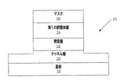
図1A乃至図1Gは、本発明の一実施形態に係るトランジスタのオーミックコンタクトの製作工程を示す模式図である。図1Aで理解されるように、窒化物ベースのデバイスを形成することができる基板10が設けられる。本発明の特定の実施形態では、基板10は、例えば、4Hポリタイプの炭化珪素である可能性のある半絶縁性炭化珪素(SiC)基板であってもよい。他の炭化珪素候補のポリタイプには、3C、6H、及び15Rポリタイプがある。用語「半絶縁性」は、絶対的な意味ではなく説明的に使用されている。本発明の特定の実施形態では、炭化珪素バルク結晶は、室温で約1×10⁵Ω−cm以上の抵抗率を有している。
1A to 1G are schematic views illustrating a process for manufacturing an ohmic contact of a transistor according to an embodiment of the present invention. As can be seen in FIG. 1A, a
随意のバッファ核形成層及び/又は遷移層(図示しない)を基板10上に設けることができる。例えば、デバイスの炭化珪素基板と残り部分の間の適切な結晶構造遷移を実現するために、AlNバッファ層を設けることができる。その上、例えば、一般的に譲渡された特許の特許文献8及び9に記載されているように、歪み釣合わせ遷移層を設けることもできる。これらの開示は、あたかも本明細書に完全に示されたかのように参照して本明細書に組み込まれる。
Optional buffer nucleation layers and / or transition layers (not shown) may be provided on the
炭化珪素は、III族窒化物デバイスの非常に一般的な基板材料であるサファイア(Al2O3)よりもIII族窒化物にずっと近い結晶格子整合を有している。このより近い格子整合は、サファイア上に一般に得ることができるものよりも高品質なIII族窒化物の膜をもたらすことができる。また、炭化珪素は、非常に高い熱伝導率を有しているので、炭化珪素上のIII族窒化物デバイスの全出力電力は、一般に、サファイア上に形成された同じデバイスの場合ほど基板の熱放散で制限されない。また、半絶縁性炭化珪素基板の有用性は、デバイス分離及び寄生キャパシタンス減少を可能にすることができる。適切なSiC基板は、例えば、本発明の譲受人であるノースカロライナ州ダラムのCree,Inc.で製造されており、そして、製造方法は、例えば特許文献10、11、12、及び13に記載されている。これらの特許の内容は、その全体を参照して本明細書に組み込まれる。同様に、III族窒化物のエピタキシャル成長の技術は、例えば特許文献14、15、16、及び17に記載されている。これらの特許の内容は、また、その全体を参照して本明細書に組み込まれる。 Silicon carbide has a crystal lattice match much closer to group III nitride than sapphire (Al 2 O 3 ), a very common substrate material for group III nitride devices. This closer lattice match can result in a higher quality III-nitride film than can generally be obtained on sapphire. Also, because silicon carbide has a very high thermal conductivity, the total output power of a III-nitride device on silicon carbide is generally higher than that of the same device formed on sapphire. It is not restricted by dissipation. Also, the availability of a semi-insulating silicon carbide substrate can allow device isolation and parasitic capacitance reduction. Suitable SiC substrates are described, for example, in Cree, Inc. of Durham, NC, the assignee of the present invention. The manufacturing method is described in, for example, Patent Documents 10, 11, 12, and 13. The contents of these patents are incorporated herein by reference in their entirety. Similarly, the technique of epitaxial growth of group III nitride is described in, for example, Patent Documents 14, 15, 16, and 17. The contents of these patents are also incorporated herein by reference in their entirety.
炭化珪素は好ましい基板材料である可能性があるが、本発明の実施形態は、サファイア、窒化アルミニウム、窒化アルミニウムガリウム、窒化ガリウム、シリコン、GaAs、LGO、ZnO、LAO、InP及び同様なものなどのどんな適切な基板でも利用することができる。いくつかの実施形態では、適切なバッファ層を形成することもできる。 Although silicon carbide may be a preferred substrate material, embodiments of the present invention include sapphire, aluminum nitride, aluminum gallium nitride, gallium nitride, silicon, GaAs, LGO, ZnO, LAO, InP, and the like. Any suitable substrate can be used. In some embodiments, a suitable buffer layer may be formed.
図1Aに戻って、チャネル層20が基板10上に設けられる。チャネル層20は、上述したようにバッファ層、遷移層、及び/又は核形成層を使用して基板10上に堆積することができる。チャネル層20は、圧縮歪みを受ける可能性がある。さらに、チャネル層及び/又はバッファ核形成層及び/又は遷移層は、MOCVDによって、又はMBE又はHVPEなどの当業者に知られている他の技術によって堆積することができる。
Returning to FIG. 1A, a
本発明のいくつかの実施形態では、チャネル層20は、チャネル層20のバンドギャップが障壁層22のバンドギャップよりも小さいという条件で、AlxGa1−xNなどのIII族窒化物である。ここで、0≦x<1である。本発明のある特定の実施形態では、x=0であり、チャネル層20がGaNであることを示している。チャネル層20は、また、InGaN、AlInGaN及び同様なものなどの他のIII族窒化物であってもよい。チャネル層20は、アンドープ(「故意でなくドープされた」)であってもよく、また、約20Åを超える厚さに成長してもよい。また、チャネル層20は、GaN、AlGaN、又は同様なものの超格子又は組合せなどの多層構造であってもよい。
In some embodiments of the present invention, the
障壁層22が、チャネル層20上に設けられる。チャネル層20は、障壁層22のバンドギャップよりも小さなバンドギャップを有することができる。障壁層22は、チャネル層20上に堆積することができる。本発明のある特定の実施形態では、障壁層22は、約1から約100nmの厚さを有するAlN、AlInN、AlGaN、又はAlInGaNである。本発明のいくつかの実施形態では、障壁層22は、多層を含んでいる。例えば、障壁層22は、約1nmのAlNであり、このAlN層上に約25nmのAlGaNがあってもよい。本発明のある特定の実施形態に従った障壁層の例は、特許文献18、Smorchkovaら、「GROUP-III NITRIDE BASED HIGH ELECTRON MOBILITY TRANSISTOR (HEMT) WITH BARRIER/SPACER LAYER」に記載されている。この出願の開示は、あたかも本明細書に完全に示されたかのように参照して本明細書に組み込まれる。
A
障壁層22は、III族窒化物であってもよく、チャネル層20のバンドギャップよりも大きなバンドギャップを有している。したがって、本発明のある特定の実施形態では、障壁層22は、AlGaN、AlInGaN及び/又はAlN又はこれらの層の組合せである。また、障壁層22に他の材料を使用することもできる。例えば、ZnGeN2、ZnSiN2及び/又はMgGeN2も使用されることができる。障壁層22は、例えば、厚さが約1から約100nmである可能性があるが、ひび割れ又は実質的な欠陥が生じるほど厚くない。好ましくは、障壁層22は、アンドープであるか、又はn型ドーパントを約1019cm−3より下の濃度にドープされている。本発明のいくつかの実施形態では、障壁層22は、AlxGa1−xNであり、0<x<1である。そのような実施形態では、障壁層22は、厚さが約3から約30nmであってもよい。特定の実施形態では、アルミニウム濃度は約25%である。しかし、本発明の他の実施形態では、障壁層22は、約5%から約100%のアルミニウム濃度を有するAlGaNを備える。本発明の特定の実施形態では、アルミニウム濃度は約10%を超える。障壁層22がAlN層を備える本発明の実施形態では、障壁層22の厚さは、例えば、約0.3nmから約4nmであってもよい。
The
図1Bは、随意の第1の誘電体層の形成工程を示す図である。第1の誘電体層24は、SixNy層などの窒化珪素層であってもよい。窒化珪素層は、デバイスの不動態化層として働くことができる。窒化珪素層は、例えば、プラズマ増速化学気相成長(PECVD)、低圧化学気相成長(LPCVD)及び/又はスパッタリングで堆積することができる。窒化珪素層は、トランジスタの他の層として同じ反応炉で堆積することができる。本発明のいくつかの実施形態では、例えば、酸窒化珪素及び/又は二酸化珪素などの他の誘電体を使用することもできる。
FIG. 1B illustrates an optional first dielectric layer formation step. The
図1Cは、第1の誘電体層上のマスクの形成工程を示す図である。マスク30は、後でゲートコンタクトが形成される障壁層22のそのような領域の上に形成される。図1Cに示すように、図1Cのウェーハは、エピ反応炉から取り出され、所望の凹部面積を露出させるようにマスク材料30を用いてパターン形成される可能性がある。マスク材料30は、以下で説明するように再成長コンタクト領域26の形成を含んだその後の処理の成長温度に耐えることができるべきである。本発明の特定の実施形態では、マスク30は、酸化物で実現される。本発明のある特定の実施形態では、マスク30は、リフトオフ技術を使用してパターン形成される。もしくは、マスク30をパターン形成するために、ウェットエッチング又はドライエッチングが利用されることができる。本発明のある特定の実施形態では、SiOxがマスク材料であるが、AlN及びSixNyベースの材料などの他の材料を使用することもできる。堆積温度又は同様なものなどのその後の処理ステップで過度に損傷を受けなければ、フォトレジスト、電子ビームレジスト材料、又は有機マスク材料を利用することもできる。
FIG. 1C is a diagram illustrating a process of forming a mask on the first dielectric layer.
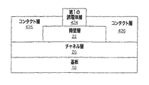
図1Dに示すように、コンタクト凹部23がオーミックコンタクトのために形成されない領域にマスク材料を残すようにマスク30を形成しパターン形成した後で、第1の誘電体層24及び障壁層22を通してチャネル層20まで、またいくつかの実施形態ではチャネル層20の中まで、又はいくつかの実施形態ではチャネル層20も通して、コンタクト凹部23がエッチングされる。このコンタクト凹部23を形成するこのエッチングは、例えば、ウェットエッチング、ドライエッチング及び/又は反応性イオンエッチング又は同様なものによって行うことができる。場合によっては、エッチングに起因する損傷を除去し、かつ/又は減少させるために、この構造をアニールすることができる。さらに、場合によっては、例えば、フィールドプレートや打込みのような他の終端構造が設けられていない場合、又はそのような終端構造に加えて設けられる可能性がある場合、メサ構造(図示しない)を形成するようにデバイスの周囲をエッチングしてもよい。
As shown in FIG. 1D, after forming and patterning a
図1Eに示すように、コンタクト凹部23をエッチングした後で、チャネル層20及びマスク30の露出された領域上にコンタクト層26’が形成される。例えば、コンタクト層26’の堆積のために図1Dのウェーハをエピ反応炉の中に再び入れることができる。本発明のいくつかの実施形態では、コンタクト層26’は、有機金属化学気相成長(MOCVD)、分子線エピタキシィ(MBE)、プラズマ増速化学気相成長(PECVD)、スパッタリング及び/又は水素化物気相エピタキシィ(HVPE)によって形成される。いくつかの実施形態では、コンタクト層26’は、下げられた堆積温度で再成長される。特に、低温堆積プロセスを使用することができる。本明細書で使用されるとき、「低温堆積」は、ウェーハから再成長領域への実質的な質量の移送が起こる温度よりも低い温度で層を形成することを意味する。例えば、コンタクト層26’は、約室温から約950℃の温度で形成することができる。いくつかの実施形態では、コンタクト層26’は、960℃より低い温度で形成される。本発明の特定の実施形態では、コンタクト層26’は、非常に低い温度で、例えば、約450℃より低い温度で形成され、さらに、いくつかの実施形態では約200℃より低い温度で形成される。そのような非常に低い温度条件は、例えば、スパッタリング及び/又はPECVD成長技術で使用される可能性がある。下げられた堆積温度及び/又は低温堆積の使用は、トラッピングを減少させる可能性があり、かつ/又は信頼性の改善を実現する可能性がある。
As shown in FIG. 1E, after the
以下で説明するように、コンタクト層26’は、マスク30上の部分が多孔性であるか不連続であるように不均一に形成することができる。いくつかの実施形態では、コンタクト層26’は、マスク30上に形成されない。そのようなコンタクト層26’の選択的な形成は、コンタクト層26’の組成、マスク30及びコンタクト層26’の成長条件に依存する可能性がある。
As will be described below, the contact layer 26 'can be non-uniformly formed such that portions on the
本発明のいくつかの実施形態では、コンタクト層26’は、n型縮退(degenerate)半導体材料であってもよい。本発明のある特定の実施形態では、コンタクト層26’は、高濃度にドープされたn型InN、InAlN、AlGaN、AlInGaN、GaN及び/又はInGaNであってもよい。本発明の他の実施形態では、コンタクト層26’は、GaN又はAlGaN以外のn型縮退半導体材料であってもよい。例えば、コンタクト層26’は、非窒化物III−V族半導体材料、IV族半導体材料及び/又はII−VI族半導体材料であってもよい。また、コンタクト層26’の可能性のある材料の例には、例えば、ZnO、ZnGeN2及び/又はZnSnN2がある。本発明の他の実施形態では、コンタクト層26’は、低い仕事関数を有しショットキコンタクトを形成しない、低温で共形堆積の可能な金属又は金属合金、例えば、金属シリサイドである可能性がある。例えば、2DEGに接するために少なくとも約200℃の温度でDMAIHを使用してAlをMOCVDで共形堆積すること。この金属は、後で、チャネル及びゲート領域で実質的にエッチング除去される可能性がある。さらに、この金属の堆積の前に、不動態化層を堆積してもよい。
In some embodiments of the present invention, the contact layer 26 'may be an n-type degenerate semiconductor material. In certain embodiments of the invention, the contact layer 26 'may be heavily doped n-type InN, InAlN, AlGaN, AlInGaN, GaN and / or InGaN. In other embodiments of the present invention, the contact layer 26 'may be an n-type degenerate semiconductor material other than GaN or AlGaN. For example, the
GaNコンタクト層26’の形成は、チャネル層20もGaNである場合、チャネル層20とのバンド不連続を減少し、かつ/又はなくする可能性がある。コンタクト層26’は、低シート抵抗率を与えるのに十分な厚さに形成される。例えば、コンタクト層26’は、チャネル層20と障壁層22の間の界面に形成された2DEGのシート抵抗率よりも小さなシート抵抗率を与えるのに十分な厚さに成長される可能性がある。例えば、数十ナノメートルのGaNは、コンタクト層26’に十分な厚さである可能性があるが、より厚い層はより低い抵抗を有し、移動長(LT)を増すことができる。コンタクト層26’は、Si、Ge及び/又はO又は他の適切なn型ドーパントをドープすることができ、又は堆積されたままでは自然にn型である可能性がある。コンタクト層26’は、その後のイオン打込みによらないで、形成されるときにドープすることができる。イオン打込みなしにドープされたコンタクト層26’の形成は、ドーパントを活性化するための極端に高い温度のアニールの必要性をなくすることができる。本発明の特定の実施形態では、コンタクト層26’は、約10から約400Ω/□のシート抵抗率を有する。本発明のある特定の実施形態では、コンタクト層26’は、約1018から約1021cm−3のキャリア濃度を与えるようにドープされる。本発明のさらに他の実施形態では、コンタクト層26’は、厚さが約10nmから約1000nmである。
Formation of the
III族窒化物材料でないコンタクト層26’では、材料は全面一括堆積され、それから堆積の後でパターン形成されエッチングされることができるので、マスク30は必要でない可能性がある。
For
図1Fは、マスク上に形成されたコンタクト層の部分を除去し、さらにマスクを除去して第1の誘電体層を露出させ、このようにしてコンタクト領域を設ける工程を示す図である。例えば、マスク30を除去し第1の誘電体層24及びコンタクト領域26を残すバッファHF又は他のエッチング液でマスク30をエッチングすることによって、マスク30及びコンタクト層26’の部分を除去することができる。本発明のいくつかの実施形態では、マスク30上に形成されたコンタクト層26’の部分は、コンタクト層26’を通してマスク30をエッチングすることを可能にするように、多孔性又は不連続であるように形成することができる。そのようにして、コンタクト層26’及び第1の誘電体層24に対してエッチング選択性を有するエッチング液で、マスク30をエッチングすることができる。より小さな形状寸法のデバイスの場合には、例えば、マスク層上のコンタクト層26’の部分が多孔性でなく又は連続であれば、マスク層30を側面からエッチングして、マスク層及びマスク層30上のコンタクト層26’の部分を除去することができる。
FIG. 1F is a diagram showing a process of removing a portion of the contact layer formed on the mask, further removing the mask to expose the first dielectric layer, and thus providing a contact region. For example, portions of the
図1Gは、第1の誘電体層24へのゲート凹部の形成及びゲート凹部の障壁層22の露出部分上へのゲートコンタクト44の形成工程を示す図である。例えば、ゲート凹部は、例えば、ドライエッチング、ウェットエッチング及び/又はRIE又は同様なものを使用して、第1の誘電体層24を通してエッチングすることができる。場合によっては、ゲート凹部のエッチングに起因する損傷の一部又は全てを修復するために、この構造をアニールすることができる。適切なゲートコンタクト材料には、例えば、Ni、Pt、Pd又は他のそのようなショットキコンタクト材料がある。また、追加の上塗り層(overlayer)を設けることもできる。本発明のいくつかの実施形態では、ゲートコンタクト44は、誘電体層24の上に形成することができる。
FIG. 1G is a diagram illustrating a process of forming a gate recess in the
図1Gでさらに理解されるように、オーミックコンタクト40及び42がコンタクト領域26の上に形成され、ソース及びドレインコンタクトを実現することができる。オーミックコンタクト40及び42は、ゲート凹部及び/又はコンタクト44の形成の前又は後に形成することができる。本発明のいくつかの実施形態では、オーミックコンタクト40及び42は、例えば、約850℃以下の温度でアニールされる。他の実施形態では、オーミックコンタクトのアニールは行われない。下げられたアニール温度を使用すること、又はアニールを使用しないことで、トラッピングを減少することができ、かつ/又は信頼性の改善を行うことができる。高濃度ドープn型コンタクト領域の存在はコンタクト抵抗を下げることができ、これは、効率及び/又は無線周波電力密度の向上を可能にすることができる。適切なオーミックコンタクト材料には、例えば、使用される可能性があるTi/Al/Ni/Auのスタックがある。同様に、Ti/Al/X/Auの構造が使用される可能性があり、XはMo、Pt及び/又はTiであってもよい。
As further understood in FIG. 1G,
本発明の実施形態は、コンタクト層26’の一面一括堆積に関連して説明したが、代わりに、依然として本発明の教示から利益を得ながら、コンタクト領域26の選択的再成長が利用されることができる。さらに、再成長コンタクト領域26は、オーミックコンタクト40及び42のうちの一方だけに設けられ、他方のコンタクトには従来のコンタクト構造が設けられることがある。したがって、本発明の実施形態は、図1A乃至図1Gに示した特定の処理ステップに限定されるように解釈されるべきでない。
Although embodiments of the present invention have been described in connection with single-sided bulk deposition of contact layer 26 ', instead, selective regrowth of
さらに、特定な順序の処理ステップを説明したが、依然として本発明の実施形態の範囲内にありながら、この順序から逸脱することができる。例えば、ゲート凹部及びゲートコンタクトは、オーミックコンタクトの形成の前又は後に、又はコンタクト凹部の形成の前でも、形成することができる。したがって、本発明の実施形態は、上述した特定の順序の工程に限定されるように解釈されるべきでない。 Furthermore, while a particular order of processing steps has been described, it is possible to deviate from this order while still remaining within the scope of embodiments of the present invention. For example, the gate recess and the gate contact can be formed before or after the ohmic contact is formed, or even before the contact recess is formed. Accordingly, embodiments of the present invention should not be construed as limited to the particular sequence of steps described above.
図2は、本発明の他の実施形態に係るトランジスタを示す模式的な構成図である。図3Aは、本発明のさらに他の実施形態に係るトランジスタを示す模式的な構成図(上面図)で、図3Bは、本発明のさらに他の実施形態に係るトランジスタを示す模式的な構成図(断面図)で、コンタクト領域26とチャネル層20の間の界面の垂直方向表面積の増加を実現するコンタクト面積拡大構造を組み込んだ本発明の実施形態の説明図である。図2は、チャネル層20の一部の側面部にコンタクト面積拡大構造を組み込むものとして本発明の実施形態を示し、図3A及び3Bは、コンタクト面積拡大構造が、チャネル層20の中に延びる充填された穴で実現されている本発明の実施形態を示す図である。コンタクト面積拡大構造の各々は、本明細書で別々に説明するが、コンタクト面積拡大構造は、また、互いに組み合わせて実現することができ、又は、チャネル層20とコンタクト領域26の間の垂直方向コンタクト面積を平面の垂直方向コンタクト面積に比べて増加させる他の構造と組み合わせて実現することができる。そのような構造は、窒化物ベースのn型半導体材料のコンタクト領域26の垂直方向部分と窒化物ベースのチャネル層20の間の界面の表面積を増加させる手段を実現することができる。
FIG. 2 is a schematic configuration diagram showing a transistor according to another embodiment of the present invention. FIG. 3A is a schematic configuration diagram (top view) showing a transistor according to still another embodiment of the present invention, and FIG. 3B is a schematic configuration diagram showing a transistor according to still another embodiment of the present invention. (Cross sectional view) is an explanatory view of an embodiment of the present invention incorporating a contact area expansion structure that realizes an increase in the vertical surface area of the interface between the contact region and the channel layer. FIG. 2 illustrates an embodiment of the present invention as incorporating a contact area expansion structure into a portion of the side surface of the
図2、図3A及び図3Bは、単一のオーミックコンタクト領域を図示するトランジスタの部分断面図である。当業者は理解するように、ソースコンタクト及びドレインコンタクトを実現するためにゲートコンタクトの反対側の第2のオーミックコンタクト領域に対して、対応する断面図を実現することができる。もしくは、本発明の実施形態は、オーミックコンタクトの1つだけにコンタクト面積拡大構造を実現することができる。 2, 3A and 3B are partial cross-sectional views of a transistor illustrating a single ohmic contact region. As those skilled in the art will appreciate, corresponding cross-sectional views can be implemented for the second ohmic contact region opposite the gate contact to implement the source and drain contacts. Alternatively, the embodiment of the present invention can realize a contact area expansion structure for only one ohmic contact.
図2は、本発明のさらに他の実施形態に係るHEMTの部分の上面図である。図2で理解されるように、チャネル層20及び/又は障壁層22の増加した表面積の側面部200を実現することによって、コンタクト領域26とチャネル層20及び/又は障壁層22との間の界面の表面積を増加させることができる。増加した表面積の側面部200は、まっすぐな側面部に比べて増加した表面積を有する。コンタクト領域26とチャネル層20の間の界面の表面積を増加させることで、コンタクト領域26とチャネル層20の間の抵抗を減少させることができる。
FIG. 2 is a top view of a HEMT portion according to still another embodiment of the present invention. As can be seen in FIG. 2, the interface between the
パターン形成された側面部200は、上述したコンタクト凹部のエッチング中にチャネル層20をパターン形成することによって実現することができる。例えば、第1の誘電体層24及び障壁層22を通して第1のエッチングを行うことができ、次に、チャネル層20の露出部分の上のマスクを用いて、チャネル層22中に第2のエッチングを行って、側面部のパターンを実現することができる。代わりに、マスク30がチャネル層20の所望の側面部パターンに対応するパターンを有している場合には、単一のエッチングを行うことができる。
The patterned
側面部は、規則的又は不規則な繰返しの形又は繰り返さない形を有することができる。図2に示す鋸歯状の形は、使用することができる形の例として与えられている。しかし、他の形、例えば、切欠きの形、一連の湾曲部又は同様なものを使用することができる。したがって、本発明のいくつかの実施形態は、増加した表面積の側面部200の特定の形に限定されるべきでない。
The side portions can have a regular or irregular repeating shape or a non-repeating shape. The serrated shape shown in FIG. 2 is given as an example of a shape that can be used. However, other shapes can be used, such as a notch shape, a series of bends, or the like. Thus, some embodiments of the present invention should not be limited to the specific shape of the increased surface
オーミックコンタクト金属42’は、また、コンタクト領域26に接して図2に示されている。コンタクト金属42’は、コンタクト領域26の周囲の前で止まるものとして示されている。しかし、コンタクト金属42’は、図示されているよりもさらに延びることができ、例えば、チャネル層22まで延びることができる。
The
図3Aは、上面図であり、図3Bは、本発明のさらに他の実施形態の図3Aの線I−I’に沿った断面図である。図3で理解されるように、再成長コンタクト領域26とチャネル層20の間の界面の表面積は、チャネル層20の中に延びる穴300を設けることによって増加させることができる。穴300には、コンタクト領域26に設けられるようなn型材料がその中にある。オーミックコンタクト42”は穴300を覆うように広がっているので、穴300の中のn型材料はコンタクト領域26に電気的に接続されている。
FIG. 3A is a top view and FIG. 3B is a cross-sectional view taken along line I-I ′ of FIG. As can be seen in FIG. 3, the surface area of the interface between the
充填された穴300は、コンタクト層26’が形成されるとき存在する穴を実現するために、上述したコンタクト凹部エッチング中にチャネル層20をパターン形成することによって実現することができる。例えば、第1の誘電体層24及び障壁層22を通して第1のエッチングを行うことができ、次に、穴を実現するためにチャネル層20の露出部分上にマスクがある状態で、チャネル層22に第2のエッチングを行うことができる。
代わりに、マスク30が、チャネル層20の所望の穴に対応するパターンを有する場合には、単一のエッチングを行うことができる。そのような場合、穴は、障壁層22を通り抜けてチャネル層20まで、又はチャネル層20の中まで延びるだろう。そのとき、コンタクト金属は、図3Bに示すように、障壁層22まで延びて穴300の中の材料に接触するだろう。
Alternatively, if the
穴300は、規則的又は不規則な繰返しパターン又は繰り返さないパターンを有することができる。さらに、穴300は、また、円形又は他の形の周囲を有することができる。図3Aに示す穴のパターン及び穴の形は、使用することができるパターン及び形の例として与えられている。しかし、他のパターン及び/又は形を使用することもできる。したがって、本発明のいくつかの実施形態は、穴300の特定のパターン及び/又は形に限定されるべきでない。
The
図4A乃至図4Cは、本発明のさらに他の実施形態に係るトランジスタの製作工程を示す模式図で、障壁層まで延びるコンタクト領域が実現された本発明のさらに他の実施形態の製作工程を示す図である。図4A乃至図4Cに示す本発明の実施形態の製作は、例えば、等方性エッチングでマスク30の下の第1の誘電体層24を切り取ることによって、障壁層22の一部を露出させるように第1の誘電体層24の大きさがより小さな大きさの第1の誘電体層424に作り直されていることを除いて、図1A乃至図1Fに示すものと同じである可能性がある。代わりに、マスク30を剥離し、別のマスクを付けてもよく、この第2のマスクを使用して第1の誘電体層24をエッチングすることができる。図4Aの第1の誘電体層424は、本明細書で誘電体材料として説明したが、コンタクト領域の堆積の条件に耐えることができる他の除去可能な材料を使用することができる。
4A to 4C are schematic views illustrating a process of manufacturing a transistor according to still another embodiment of the present invention, and illustrate a process of manufacturing another embodiment of the present invention in which a contact region extending to a barrier layer is realized. FIG. The fabrication of the embodiment of the invention shown in FIGS. 4A-4C may expose a portion of the
図4Aで理解されるように、コンタクト領域426が上述したように再成長され、マスク30が除去される。図4Bで理解されるように、第1の誘電体層424が除去され、第2の誘電体層430がコンタクト層426及び障壁層22上に共形的に堆積される。第2の誘電体層430は、一般に、等方的に堆積されるだろう。第2の誘電体層430の窓をコンタクト層426上に設けることができ、また、ソース及びドレインコンタクト440及び442のためのオーミックコンタクトをコンタクト層426上に形成することができる。オーミックコンタクトは、また、第2の誘電体層430の堆積より前に形成することもできる。
As can be seen in FIG. 4A,
図4Cで理解されるように、障壁層22を露出させ、かつ側面部スペーサ430’及びゲートコンタクト凹部を設けるように、第2の誘電体層430が異方性エッチングされる。例えば、リフトオフ技術を使用して、ゲート金属を堆積し、パターン形成して、ゲートコンタクト444を実現することができる。ゲートコンタクト444の長さは、第2の誘電体層430の厚さの2分の1のほぼ第1の誘電体層424の幅であってもよい。本発明の特定の実施形態では、第1の誘電体424は、約0.5から約1μmの幅を有することができ、第2の誘電体430は、約0.1から約0.5μmの厚さを有することができる。
As can be seen in FIG. 4C, the
本発明の実施形態は、ソースコンタクトとドレインコンタクトの両方の再成長コンタクト領域に関して説明したが、そのような再成長領域は、ソース又はドレインのただ一方だけに設けることができる。さらに、ゲートコンタクトは、ソースとドレインの間の実質的に中心に位置付けされるように説明したが、本発明のある特定の実施形態では、ゲートコンタクトは、例えば、ソースコンタクトの方に片寄っていることがある。 Although embodiments of the present invention have been described with respect to regrowth contact regions for both source and drain contacts, such regrowth regions can be provided in only one of the source or drain. Further, although the gate contact has been described as being substantially centered between the source and drain, in certain embodiments of the invention, the gate contact is offset, for example, toward the source contact. Sometimes.
さらに、本発明の実施形態は特定の順序の製作ステップに関連して説明したが、依然として本発明の技術的範囲内に含まれながら異なった順序のステップが利用される可能性がある。したがって、本発明の実施形態は、本明細書で説明した特定の順序に限定されるように解釈されるべきでない。 Further, although embodiments of the present invention have been described with reference to a particular sequence of fabrication steps, different sequences of steps may still be utilized while still falling within the scope of the present invention. Accordingly, embodiments of the present invention should not be construed as limited to the specific order set forth herein.
図面及び明細書で、本発明の代表的な実施形態が開示され、特定の用語が使用されたが、これらの用語は一般的な記述的な意味でだけ使用され、限定の目的のために使用されていないので、本発明の技術的範囲は添付の特許請求の範囲に示される。 In the drawings and specification, there have been disclosed exemplary embodiments of the invention and specific terminology has been used, but these terms are used in a generic and descriptive sense only and are used for the purpose of limitation. Therefore, the technical scope of the present invention is set forth in the appended claims.
Claims (56)
前記窒化物ベースのチャネル層上に障壁層を提供するステップと、
前記窒化物ベースのチャネル層のコンタクト領域を露出させるように、前記障壁層を越えて前記チャネル層の中に延びるコンタクト凹部を提供するステップと、
前記チャネル層と前記コンタクト領域上のn型コンタクト層との間に平面界面に比べて増加した表面積の界面を設けるように前記チャネル層の側面部を提供するステップと、
低温堆積プロセスを使用して、前記窒化物ベースのチャネル層の前記露出されたコンタクト領域上に前記n型コンタクト層を提供するステップと、
前記n型コンタクト層上にオーミックコンタクトを提供するステップと、
前記オーミックコンタクトに隣接した前記障壁層上に配置されるゲートコンタクトを提供するステップと
を有し、
前記低温堆積プロセスは450℃より低い温度であることを特徴とするトランジスタの製作方法。Providing a nitride-based channel layer;
Providing a barrier layer on the nitride-based channel layer;
Providing a contact recess extending into the channel layer beyond the barrier layer to expose a contact region of the nitride-based channel layer;
Providing a side portion of the channel layer to provide an interface with an increased surface area compared to a planar interface between the channel layer and an n-type contact layer on the contact region;
Providing the n-type contact layer on the exposed contact region of the nitride-based channel layer using a low temperature deposition process;
Providing an ohmic contact on the n-type contact layer;
Providing a gate contact disposed on the barrier layer adjacent to the ohmic contact;
The method of manufacturing a transistor, wherein the low temperature deposition process is performed at a temperature lower than 450 ° C.
前記第1の誘電体層にゲート凹部を提供するステップとを有し、
前記ゲートコンタクトを提供するステップは、前記ゲート凹部の中にゲートコンタクトを提供し、
前記コンタクト凹部を提供するステップは、前記窒化物ベースのチャネル層の部分を露出させるオーミックコンタクト凹部を前記第1の誘電体層及び前記障壁層に提供することを特徴とする請求項1に記載のトランジスタの製作方法。Providing a first dielectric layer on the barrier layer;
Providing a gate recess in the first dielectric layer;
Providing the gate contact provides a gate contact in the gate recess;
The method of claim 1, wherein providing the contact recess comprises providing an ohmic contact recess in the first dielectric layer and the barrier layer exposing a portion of the nitride-based channel layer. Transistor fabrication method.
前記ゲートコンタクトを提供するステップは、前記第1の誘電体層上にゲートコンタクトを形成し、
前記コンタクト凹部を提供するステップは、前記窒化物ベースのチャネル層の部分を露出させるオーミックコンタクト凹部を前記第1の誘電体層及び前記障壁層に提供することを特徴とする請求項1に記載のトランジスタの製作方法。Providing a first dielectric layer on the barrier layer;
Providing the gate contact includes forming a gate contact on the first dielectric layer;
The method of claim 1, wherein providing the contact recess comprises providing an ohmic contact recess in the first dielectric layer and the barrier layer exposing a portion of the nitride-based channel layer. Transistor fabrication method.
前記n型コンタクト層上の金属層をパターン形成し、
前記パターン形成された金属層を850℃以下の温度でアニールすることを特徴とする請求項1に記載のトランジスタの製作方法。Providing the ohmic contact comprises:
Patterning a metal layer on the n-type contact layer;
The method of claim 1, wherein the patterned metal layer is annealed at a temperature of 850 ° C. or less.
前記穴の中に窒化物ベースのn型半導体材料を入れるステップとを有し、
前記n型コンタクト層上にオーミックコンタクトを提供するステップは、前記n型コンタクト層及び前記穴の中の前記窒化物ベースのn型半導体材料にオーミックコンタクトを提供することを特徴とする請求項1に記載のトランジスタの製作方法。Providing a hole in the channel layer adjacent to the contact region;
Placing a nitride-based n-type semiconductor material in the hole;
The step of providing an ohmic contact on the n-type contact layer provides an ohmic contact to the n-type contact layer and the nitride-based n-type semiconductor material in the hole. A manufacturing method of the transistor described.
前記窒化物ベースのチャネル層の第2のコンタクト領域を露出させるように前記障壁層に第2のコンタクト凹部を提供するステップと、
低温堆積プロセスを使用して、前記窒化物ベースのチャネル層の前記露出された第2のコンタクト領域上にコンタクト層を提供するステップと、
前記コンタクト層上に第2のオーミックコンタクトを提供するステップとを有し、
前記ゲートコンタクトを提供するステップが、前記第1と第2のオーミックコンタクトの間の前記障壁層上に配置されたゲートコンタクトを提供することを特徴とする請求項1に記載のトランジスタの製作方法。The contact recess includes a first contact recess, the contact region includes a first contact region, the ohmic contact includes a first ohmic contact, and the method further includes:
Providing a second contact recess in the barrier layer to expose a second contact region of the nitride-based channel layer;
Providing a contact layer on the exposed second contact region of the nitride-based channel layer using a low temperature deposition process;
Providing a second ohmic contact on the contact layer;
The method of claim 1, wherein providing the gate contact comprises providing a gate contact disposed on the barrier layer between the first and second ohmic contacts.
前記障壁層上にマスク層を提供し、
前記窒化物ベースのチャネル層の部分を露出させる前記コンタクト凹部を設けるために前記マスク層及び前記障壁層をパターン形成し、
前記n型コンタクト層を提供するステップは、前記窒化物ベースのチャネル層の前記露出された部分及び前記マスク層上にn型コンタクト層を提供し、前記方法は、前記窒化物ベースのチャネル層のコンタクト領域を設けるために前記マスク層及び前記マスク層上の前記n型コンタクト層の部分を選択的に除去することを特徴とする請求項1に記載のトランジスタの製作方法。The step of providing the contact recess comprises:
Providing a mask layer on the barrier layer;
Patterning the mask layer and the barrier layer to provide the contact recess exposing a portion of the nitride-based channel layer;
The step of providing the n-type contact layer provides n-type contact layer on the exposed portion and the mask layer of the nitride-based channel layer, said method of the nitride-based channel layer 2. The method of manufacturing a transistor according to claim 1, wherein a portion of the mask layer and the n-type contact layer on the mask layer is selectively removed to provide a contact region.
前記第1の誘電体層に凹部を提供するステップとを有し、
前記ゲートコンタクトを提供するステップは、前記凹部にゲートコンタクトを提供し、
前記障壁層上にマスク層を提供するステップは、前記第1の誘電体層上にマスク層を提供し、
前記窒化物ベースのチャネル層の部分を露出させるコンタクト凹部を設けるために前記マスク層及び前記障壁層をパターン形成するステップは、前記窒化物ベースのチャネル層の部分を露出させるコンタクト凹部を設けるために、前記マスク層、前記第1の誘電体層及び前記障壁層をパターン形成することを特徴とする請求項21に記載のトランジスタの製作方法。Providing a first dielectric layer on the barrier layer;
Providing a recess in the first dielectric layer;
Providing the gate contact provides a gate contact in the recess;
Providing a mask layer on the barrier layer provides a mask layer on the first dielectric layer;
Patterning the mask layer and the barrier layer to provide a contact recess exposing a portion of the nitride-based channel layer to provide a contact recess exposing a portion of the nitride-based channel layer; The method of claim 21 , wherein the mask layer, the first dielectric layer, and the barrier layer are patterned.
前記窒化物ベースのコンタクト領域上の金属層をパターン形成し、
前記パターン形成された金属層を850℃より低い温度でアニールすることを特徴とする請求項21に記載のトランジスタの製作方法。Providing the ohmic contact comprises:
Patterning a metal layer on the nitride-based contact region;
The method of claim 21 , wherein the patterned metal layer is annealed at a temperature lower than 850 ° C.
前記n型コンタクト層を提供するステップは、前記穴の中に窒化物ベースの半導体材料を入れることをさらに含み、
前記窒化物ベースのコンタクト領域の上にオーミックコンタクトを提供するステップは、前記窒化物ベースのコンタクト領域、及び前記穴の中の前記窒化物ベースの半導体材料にオーミックコンタクトを提供することを特徴とする請求項21に記載のトランジスタの製作方法。Providing a hole in the channel layer adjacent to the contact region;
Providing the n-type contact layer further comprises placing a nitride-based semiconductor material in the hole;
Providing an ohmic contact over the nitride based contact region provides an ohmic contact to the nitride based contact region and the nitride based semiconductor material in the hole. The method for manufacturing a transistor according to claim 21 .
前記窒化物ベースのチャネル層の部分を露出させる第2のコンタクト凹部を設けるために前記マスク層及び前記障壁層をパターン形成するステップと、
前記第2のコンタクト凹部によって露出された前記窒化物ベースのチャネル層の前記部分上にコンタクト層を提供するステップと、
前記第2の窒化物ベースのコンタクト領域上に第2のオーミックコンタクトを提供するステップとを有し、
前記マスク層を選択的に除去する前記ステップは、前記第1の窒化物ベースのコンタクト領域及び第2の窒化物ベースのコンタクト領域を設けるために前記マスク層及び前記マスク層上の前記コンタクト層の部分を選択的に除去し、
ゲートコンタクトを提供する前記ステップは、前記第1と第2のオーミックコンタクトの間の前記障壁層上に配置されたゲートコンタクトを提供することを特徴とする請求項21に記載のトランジスタの製作方法。The contact recess includes a first contact recess, the nitride-based contact region includes a first nitride-based contact region, the ohmic contact includes a first ohmic contact, and the method includes:
Patterning the mask layer and the barrier layer to provide a second contact recess exposing a portion of the nitride-based channel layer;
Providing a contact layer on the portion of the nitride-based channel layer exposed by the second contact recess;
Providing a second ohmic contact on the second nitride-based contact region;
The step of selectively removing the mask layer includes the step of forming the first nitride-based contact region and the second nitride-based contact region on the mask layer and the contact layer on the mask layer. Selectively remove parts,
The method of claim 21 , wherein the step of providing a gate contact provides a gate contact disposed on the barrier layer between the first and second ohmic contacts.
前記窒化物ベースのチャネル層上の障壁層と、
前記チャネル層の中まで延びる、前記障壁層の少なくとも1つのコンタクト凹部と、
前記コンタクト凹部中の前記窒化物ベースのチャネル層上の、低温堆積プロセスを使用して提供されるコンタクト領域と、
前記障壁層上に配置されたゲートコンタクトとを備え、
前記コンタクト領域及び前記窒化物ベースのチャネル層が、表面積拡大構造を含み、
前記表面積拡大構造は、前記コンタクト領域の垂直部分と前記窒化物ベースのチャネル層との間の界面の表面積を平面界面に比べて増加させる手段をさらに備えることを特徴とする高電子移動度トランジスタ。A nitride-based channel layer;
A barrier layer on the nitride-based channel layer;
At least one contact recess in the barrier layer extending into the channel layer;
A contact region provided using a low temperature deposition process on the nitride-based channel layer in the contact recess;
A gate contact disposed on the barrier layer,
The contact region and the nitride-based channel layer, viewed contains a surface area enlargement structure,
The high electron mobility transistor further comprises means for increasing a surface area of an interface between a vertical portion of the contact region and the nitride-based channel layer as compared with a planar interface .
前記n型縮退半導体材料の領域上のオートミックコンタクトをさらに備えることを特徴とする請求項35に記載の高電子移動度トランジスタ。The contact region includes a region of n-type degenerate semiconductor material other than GaN or AlGaN on the nitride-based channel layer in the at least one contact recess, and an automic on the region of the n-type degenerate semiconductor material 36. The high electron mobility transistor of claim 35 , further comprising a contact.
前記障壁層は、前記窒化物ベースのチャネル層の第1の表面に近接した第2の表面を有し、
前記n型コンタクト層を提供するステップは、前記窒化物ベースのチャネル層の第1の表面と前記障壁層の第2の表面の間に直接には、意図的には挟まれていないように、前記n型コンタクト層を提供することを特徴とする請求項1に記載のトランジスタの製作方法。Providing a barrier layer provides a barrier layer on the first surface of the nitride-based channel layer;
The barrier layer has a second surface proximate to the first surface of the nitride-based channel layer;
Providing the n-type contact layer is not intentionally sandwiched directly between the first surface of the nitride-based channel layer and the second surface of the barrier layer, The method of claim 1, wherein the n-type contact layer is provided.
Applications Claiming Priority (3)
| Application Number | Priority Date | Filing Date | Title |
|---|---|---|---|
| US10/849,617 | 2004-05-20 | ||
| US10/849,617 US7432142B2 (en) | 2004-05-20 | 2004-05-20 | Methods of fabricating nitride-based transistors having regrown ohmic contact regions |
| PCT/US2005/004039 WO2005119787A1 (en) | 2004-05-20 | 2005-02-09 | Methods of fabricating nitride-based transistors having regrown ohmic contact regions and nitride-based transistors having regrown ohmic contact regions |
Publications (3)
| Publication Number | Publication Date |
|---|---|
| JP2007538402A JP2007538402A (en) | 2007-12-27 |
| JP2007538402A5 JP2007538402A5 (en) | 2008-03-21 |
| JP5160225B2 true JP5160225B2 (en) | 2013-03-13 |
Family
ID=34961328
Family Applications (1)
| Application Number | Title | Priority Date | Filing Date |
|---|---|---|---|
| JP2007527194A Active JP5160225B2 (en) | 2004-05-20 | 2005-02-09 | Method for fabricating nitride-based transistor with regrowth ohmic contact region and nitride-based transistor with regrowth ohmic contact region |
Country Status (8)
| Country | Link |
|---|---|
| US (1) | US7432142B2 (en) |
| EP (1) | EP1747589B1 (en) |
| JP (1) | JP5160225B2 (en) |
| KR (1) | KR20070032701A (en) |
| CN (1) | CN1998085B (en) |
| CA (1) | CA2567066A1 (en) |
| TW (1) | TW200539264A (en) |
| WO (1) | WO2005119787A1 (en) |
Families Citing this family (152)
| Publication number | Priority date | Publication date | Assignee | Title |
|---|---|---|---|---|
| EP2267784B1 (en) * | 2001-07-24 | 2020-04-29 | Cree, Inc. | INSULATING GATE AlGaN/GaN HEMT |
| US8809867B2 (en) * | 2002-04-15 | 2014-08-19 | The Regents Of The University Of California | Dislocation reduction in non-polar III-nitride thin films |
| KR101167590B1 (en) * | 2002-04-15 | 2012-07-27 | 더 리전츠 오브 더 유니버시티 오브 캘리포니아 | Non-polar A-plane Gallium Nitride Thin Films Grown by Metalorganic Chemical Vapor Deposition |
| US7612390B2 (en) | 2004-02-05 | 2009-11-03 | Cree, Inc. | Heterojunction transistors including energy barriers |
| JP4889203B2 (en) * | 2004-04-21 | 2012-03-07 | 新日本無線株式会社 | Nitride semiconductor device and manufacturing method thereof |
| US20080163814A1 (en) * | 2006-12-12 | 2008-07-10 | The Regents Of The University Of California | CRYSTAL GROWTH OF M-PLANE AND SEMIPOLAR PLANES OF (Al, In, Ga, B)N ON VARIOUS SUBSTRATES |
| US7709859B2 (en) * | 2004-11-23 | 2010-05-04 | Cree, Inc. | Cap layers including aluminum nitride for nitride-based transistors |
| US7456443B2 (en) * | 2004-11-23 | 2008-11-25 | Cree, Inc. | Transistors having buried n-type and p-type regions beneath the source region |
| JP4940557B2 (en) * | 2005-02-08 | 2012-05-30 | 日本電気株式会社 | Field effect transistor and manufacturing method thereof |
| CN101845670A (en) * | 2005-03-10 | 2010-09-29 | 加利福尼亚大学董事会 | The technology that is used for the growth of planar semi-polar gallium nitride |
| US20060226442A1 (en) | 2005-04-07 | 2006-10-12 | An-Ping Zhang | GaN-based high electron mobility transistor and method for making the same |
| TWI377602B (en) * | 2005-05-31 | 2012-11-21 | Japan Science & Tech Agency | Growth of planar non-polar {1-100} m-plane gallium nitride with metalorganic chemical vapor deposition (mocvd) |
| TW200703463A (en) * | 2005-05-31 | 2007-01-16 | Univ California | Defect reduction of non-polar and semi-polar III-nitrides with sidewall lateral epitaxial overgrowth (SLEO) |
| JP5743127B2 (en) * | 2005-06-01 | 2015-07-01 | ザ リージェンツ オブ ザ ユニバーシティ オブ カリフォルニア | Method and apparatus for growth and fabrication of semipolar (Ga, Al, In, B) N thin films, heterostructures and devices |
| US9331192B2 (en) | 2005-06-29 | 2016-05-03 | Cree, Inc. | Low dislocation density group III nitride layers on silicon carbide substrates and methods of making the same |
| US8148244B2 (en) * | 2005-07-13 | 2012-04-03 | The Regents Of The University Of California | Lateral growth method for defect reduction of semipolar nitride films |
| US20070018198A1 (en) * | 2005-07-20 | 2007-01-25 | Brandes George R | High electron mobility electronic device structures comprising native substrates and methods for making the same |
| KR101347848B1 (en) * | 2005-09-09 | 2014-01-06 | 재팬 사이언스 앤드 테크놀로지 에이젼시 | Method for enhancing growth of semi-polar (Al,In,Ga,B)N via metalorganic chemical vapor deposition |
| US7338826B2 (en) * | 2005-12-09 | 2008-03-04 | The United States Of America As Represented By The Secretary Of The Navy | Silicon nitride passivation with ammonia plasma pretreatment for improving reliability of AlGaN/GaN HEMTs |
| KR20080098039A (en) * | 2006-01-20 | 2008-11-06 | 더 리전츠 오브 더 유니버시티 오브 캘리포니아 | Method for enhancing growth of semipolar (al,in,ga,b)n via metalorganic chemical vapor depositon |
| KR101510461B1 (en) | 2006-01-20 | 2015-04-08 | 더 리전츠 오브 더 유니버시티 오브 캘리포니아 | Method for improved growth of semipolar (Al,In,Ga,B)N |
| EP1984940A4 (en) | 2006-02-10 | 2010-11-10 | Univ California | Method for conductivity control of (al,in,ga,b)n |
| US7388236B2 (en) * | 2006-03-29 | 2008-06-17 | Cree, Inc. | High efficiency and/or high power density wide bandgap transistors |
| US20100095882A1 (en) * | 2008-10-16 | 2010-04-22 | Tadao Hashimoto | Reactor design for growing group iii nitride crystals and method of growing group iii nitride crystals |
| US8764903B2 (en) * | 2009-05-05 | 2014-07-01 | Sixpoint Materials, Inc. | Growth reactor for gallium-nitride crystals using ammonia and hydrogen chloride |
| US8253221B2 (en) * | 2007-09-19 | 2012-08-28 | The Regents Of The University Of California | Gallium nitride bulk crystals and their growth method |
| US9803293B2 (en) * | 2008-02-25 | 2017-10-31 | Sixpoint Materials, Inc. | Method for producing group III-nitride wafers and group III-nitride wafers |
| KR20090018106A (en) * | 2006-05-09 | 2009-02-19 | 더 리전츠 오브 더 유니버시티 오브 캘리포니아 | In-situ defect reduction techniques for nonpolar and semipolar (al, ga, in)n |
| US9040398B2 (en) * | 2006-05-16 | 2015-05-26 | Cree, Inc. | Method of fabricating seminconductor devices including self aligned refractory contacts |
| JP5179023B2 (en) * | 2006-05-31 | 2013-04-10 | パナソニック株式会社 | Field effect transistor |
| US20080078439A1 (en) * | 2006-06-23 | 2008-04-03 | Michael Grundmann | Polarization-induced tunnel junction |
| WO2008021403A2 (en) * | 2006-08-16 | 2008-02-21 | The Regents Of The University Of California | Method for deposition of magnesium doped (al, in, ga, b)n layers |
| US8823057B2 (en) | 2006-11-06 | 2014-09-02 | Cree, Inc. | Semiconductor devices including implanted regions for providing low-resistance contact to buried layers and related devices |
| US8193020B2 (en) * | 2006-11-15 | 2012-06-05 | The Regents Of The University Of California | Method for heteroepitaxial growth of high-quality N-face GaN, InN, and AlN and their alloys by metal organic chemical vapor deposition |
| WO2008060349A2 (en) * | 2006-11-15 | 2008-05-22 | The Regents Of The University Of California | Method for heteroepitaxial growth of high-quality n-face gan, inn, and ain and their alloys by metal organic chemical vapor deposition |
| US7692263B2 (en) | 2006-11-21 | 2010-04-06 | Cree, Inc. | High voltage GaN transistors |
| US8878245B2 (en) * | 2006-11-30 | 2014-11-04 | Cree, Inc. | Transistors and method for making ohmic contact to transistors |
| TWI492411B (en) * | 2006-12-11 | 2015-07-11 | Univ California | Non-polar and semi-polar light emitting devices |
| TWI533351B (en) | 2006-12-11 | 2016-05-11 | 美國加利福尼亞大學董事會 | Metalorganic chemical vapor deposition (mocvd) growth of high performance non-polar iii-nitride optical devices |
| US9076852B2 (en) * | 2007-01-19 | 2015-07-07 | International Rectifier Corporation | III nitride power device with reduced QGD |
| JP4876927B2 (en) * | 2007-01-22 | 2012-02-15 | 住友電気工業株式会社 | Method for forming a semiconductor device |
| US8021904B2 (en) * | 2007-02-01 | 2011-09-20 | Cree, Inc. | Ohmic contacts to nitrogen polarity GaN |
| JP2010518626A (en) * | 2007-02-12 | 2010-05-27 | ザ リージェンツ オブ ザ ユニバーシティ オブ カリフォルニア | Optimization of laser rod orientation for nonpolar and semipolar (Ga, Al, In, B) N diode lasers |
| WO2008100504A1 (en) * | 2007-02-12 | 2008-08-21 | The Regents Of The University Of California | Cleaved facet (ga,al,in)n edge-emitting laser diodes grown on semipolar {11-2n} bulk gallium nitride substrates |
| WO2008112185A1 (en) * | 2007-03-09 | 2008-09-18 | The Regents Of The University Of California | Method to fabricate iii-n field effect transistors using ion implantation with reduced dopant activation and damage recovery temperature |
| US8212290B2 (en) * | 2007-03-23 | 2012-07-03 | Cree, Inc. | High temperature performance capable gallium nitride transistor |
| FR2914500B1 (en) * | 2007-03-30 | 2009-11-20 | Picogiga Internat | IMPROVED OHMICALLY CONTACT ELECTRONIC DEVICE |
| US9484499B2 (en) * | 2007-04-20 | 2016-11-01 | Cree, Inc. | Transparent ohmic contacts on light emitting diodes with carrier substrates |
| JP2010526444A (en) * | 2007-05-01 | 2010-07-29 | ザ リージェンツ オブ ザ ユニバーシティ オブ カリフォルニア | Light emitting diode device layer structure using indium gallium nitride contact layer |
| TWI339444B (en) | 2007-05-30 | 2011-03-21 | Au Optronics Corp | Conductor structure, pixel structure, and methods of forming the same |
| JP2009010107A (en) * | 2007-06-27 | 2009-01-15 | Oki Electric Ind Co Ltd | Semiconductor device and manufacturing method therefor |
| JP5202897B2 (en) * | 2007-07-25 | 2013-06-05 | 住友電工デバイス・イノベーション株式会社 | Field effect transistor and manufacturing method thereof |
| JP2010536182A (en) * | 2007-08-08 | 2010-11-25 | ザ リージェンツ オブ ザ ユニバーシティ オブ カリフォルニア | Nonpolar III-nitride light emitting diodes with long wavelength radiation |
| US20090039356A1 (en) * | 2007-08-08 | 2009-02-12 | The Regents Of The University Of California | Planar nonpolar m-plane group iii-nitride films grown on miscut substrates |
| US7875537B2 (en) * | 2007-08-29 | 2011-01-25 | Cree, Inc. | High temperature ion implantation of nitride based HEMTs |
| JP2010539732A (en) | 2007-09-19 | 2010-12-16 | ザ リージェンツ オブ ザ ユニバーシティ オブ カリフォルニア | Method for increasing the area of nonpolar and semipolar nitride substrates |
| KR20100064383A (en) | 2007-09-19 | 2010-06-14 | 더 리전츠 오브 더 유니버시티 오브 캘리포니아 | (al, in, ga, b)n device structures on a patterned substrate |
| US8368100B2 (en) | 2007-11-14 | 2013-02-05 | Cree, Inc. | Semiconductor light emitting diodes having reflective structures and methods of fabricating same |
| US7750370B2 (en) * | 2007-12-20 | 2010-07-06 | Northrop Grumman Space & Mission Systems Corp. | High electron mobility transistor having self-aligned miniature field mitigating plate on a protective dielectric layer |
| KR20100107054A (en) | 2008-02-01 | 2010-10-04 | 더 리전츠 오브 더 유니버시티 오브 캘리포니아 | Enhancement of optical polarization of nitride light-emitting diodes by wafer off-axis cut |
| US8519438B2 (en) | 2008-04-23 | 2013-08-27 | Transphorm Inc. | Enhancement mode III-N HEMTs |
| US9711633B2 (en) * | 2008-05-09 | 2017-07-18 | Cree, Inc. | Methods of forming group III-nitride semiconductor devices including implanting ions directly into source and drain regions and annealing to activate the implanted ions |
| EP2281076A1 (en) | 2008-06-04 | 2011-02-09 | Sixpoint Materials, Inc. | Methods for producing improved crystallinty group iii-nitride crystals from initial group iii-nitride seed by ammonothermal growth |
| WO2009149300A1 (en) * | 2008-06-04 | 2009-12-10 | Sixpoint Materials | High-pressure vessel for growing group iii nitride crystals and method of growing group iii nitride crystals using high-pressure vessel and group iii nitride crystal |
| WO2009151642A1 (en) * | 2008-06-12 | 2009-12-17 | Sixpoint Materials, Inc. | Method for testing group-iii nitride wafers and group iii-nitride wafers with test data |
| US8384115B2 (en) * | 2008-08-01 | 2013-02-26 | Cree, Inc. | Bond pad design for enhancing light extraction from LED chips |
| US8289065B2 (en) | 2008-09-23 | 2012-10-16 | Transphorm Inc. | Inductive load power switching circuits |
| WO2010053964A1 (en) * | 2008-11-07 | 2010-05-14 | The Regents Of The University Of California | Novel vessel designs and relative placements of the source material and seed crystals with respect to the vessel for the ammonothermal growth of group-iii nitride crystals |
| WO2010060034A1 (en) * | 2008-11-24 | 2010-05-27 | Sixpoint Materials, Inc. | METHODS FOR PRODUCING GaN NUTRIENT FOR AMMONOTHERMAL GROWTH |
| US7898004B2 (en) | 2008-12-10 | 2011-03-01 | Transphorm Inc. | Semiconductor heterostructure diodes |
| JP5737948B2 (en) * | 2008-12-26 | 2015-06-17 | ルネサスエレクトロニクス株式会社 | Heterojunction field effect transistor, method of manufacturing heterojunction field transistor, and electronic device |
| US7759142B1 (en) | 2008-12-31 | 2010-07-20 | Intel Corporation | Quantum well MOSFET channels having uni-axial strain caused by metal source/drains, and conformal regrowth source/drains |
| US8741715B2 (en) * | 2009-04-29 | 2014-06-03 | Cree, Inc. | Gate electrodes for millimeter-wave operation and methods of fabrication |
| US8742459B2 (en) | 2009-05-14 | 2014-06-03 | Transphorm Inc. | High voltage III-nitride semiconductor devices |
| US20100309943A1 (en) * | 2009-06-05 | 2010-12-09 | The Regents Of The University Of California | LONG WAVELENGTH NONPOLAR AND SEMIPOLAR (Al,Ga,In)N BASED LASER DIODES |
| US8268707B2 (en) * | 2009-06-22 | 2012-09-18 | Raytheon Company | Gallium nitride for liquid crystal electrodes |
| JP5580009B2 (en) * | 2009-08-28 | 2014-08-27 | 日本碍子株式会社 | Epitaxial substrate for semiconductor element, semiconductor element, and method for producing epitaxial substrate for semiconductor element |
| US8390000B2 (en) | 2009-08-28 | 2013-03-05 | Transphorm Inc. | Semiconductor devices with field plates |
| JP5609055B2 (en) * | 2009-10-02 | 2014-10-22 | 富士通株式会社 | Compound semiconductor device and manufacturing method thereof |
| US8389977B2 (en) | 2009-12-10 | 2013-03-05 | Transphorm Inc. | Reverse side engineered III-nitride devices |
| US8936976B2 (en) * | 2009-12-23 | 2015-01-20 | Intel Corporation | Conductivity improvements for III-V semiconductor devices |
| US8633470B2 (en) * | 2009-12-23 | 2014-01-21 | Intel Corporation | Techniques and configurations to impart strain to integrated circuit devices |
| US8242510B2 (en) * | 2010-01-28 | 2012-08-14 | Intersil Americas Inc. | Monolithic integration of gallium nitride and silicon devices and circuits, structure and method |
| KR101774933B1 (en) * | 2010-03-02 | 2017-09-06 | 삼성전자 주식회사 | High Electron Mobility Transistor representing dual depletion and method of manufacturing the same |
| US20110241020A1 (en) * | 2010-03-31 | 2011-10-06 | Triquint Semiconductor, Inc. | High electron mobility transistor with recessed barrier layer |
| CN102576727B (en) * | 2010-06-23 | 2016-01-27 | 康奈尔大学 | Gated III-V semiconductor structure and method |
| US9070851B2 (en) | 2010-09-24 | 2015-06-30 | Seoul Semiconductor Co., Ltd. | Wafer-level light emitting diode package and method of fabricating the same |
| US8742460B2 (en) | 2010-12-15 | 2014-06-03 | Transphorm Inc. | Transistors with isolation regions |
| JP5654884B2 (en) * | 2011-01-26 | 2015-01-14 | 株式会社東芝 | Manufacturing method of nitride semiconductor device |
| US8643062B2 (en) | 2011-02-02 | 2014-02-04 | Transphorm Inc. | III-N device structures and methods |
| US20120204957A1 (en) * | 2011-02-10 | 2012-08-16 | David Nicholls | METHOD FOR GROWING AlInGaN LAYER |
| US8772842B2 (en) | 2011-03-04 | 2014-07-08 | Transphorm, Inc. | Semiconductor diodes with low reverse bias currents |
| US8716141B2 (en) | 2011-03-04 | 2014-05-06 | Transphorm Inc. | Electrode configurations for semiconductor devices |
| US8383471B1 (en) * | 2011-04-11 | 2013-02-26 | Hrl Laboratories, Llc | Self aligned sidewall gate GaN HEMT |
| WO2013089843A2 (en) * | 2011-09-02 | 2013-06-20 | The California Institute Of Technology | Photovoltaic semiconductive materials |
| US8901604B2 (en) | 2011-09-06 | 2014-12-02 | Transphorm Inc. | Semiconductor devices with guard rings |
| US9257547B2 (en) | 2011-09-13 | 2016-02-09 | Transphorm Inc. | III-N device structures having a non-insulating substrate |
| CN103000692A (en) * | 2011-09-14 | 2013-03-27 | 鸿富锦精密工业(深圳)有限公司 | Thin-film transistor structure and manufacturing method thereof |
| US8697505B2 (en) * | 2011-09-15 | 2014-04-15 | Taiwan Semiconductor Manufacturing Company, Ltd. | Method of forming a semiconductor structure |
| US8598937B2 (en) | 2011-10-07 | 2013-12-03 | Transphorm Inc. | High power semiconductor electronic components with increased reliability |
| US20130105817A1 (en) | 2011-10-26 | 2013-05-02 | Triquint Semiconductor, Inc. | High electron mobility transistor structure and method |
| US8946771B2 (en) * | 2011-11-09 | 2015-02-03 | Taiwan Semiconductor Manufacturing Co., Ltd. | Gallium nitride semiconductor devices and method making thereof |
| US8884308B2 (en) * | 2011-11-29 | 2014-11-11 | Taiwan Semiconductor Manufacturing Company, Ltd. | High electron mobility transistor structure with improved breakdown voltage performance |
| US9165766B2 (en) | 2012-02-03 | 2015-10-20 | Transphorm Inc. | Buffer layer structures suited for III-nitride devices with foreign substrates |
| US9093366B2 (en) | 2012-04-09 | 2015-07-28 | Transphorm Inc. | N-polar III-nitride transistors |
| US9666705B2 (en) * | 2012-05-14 | 2017-05-30 | Infineon Technologies Austria Ag | Contact structures for compound semiconductor devices |
| US9184275B2 (en) | 2012-06-27 | 2015-11-10 | Transphorm Inc. | Semiconductor devices with integrated hole collectors |
| US9076850B2 (en) | 2012-07-30 | 2015-07-07 | Samsung Electronics Co., Ltd. | High electron mobility transistor |
| US9076763B2 (en) * | 2012-08-13 | 2015-07-07 | Infineon Technologies Austria Ag | High breakdown voltage III-nitride device |
| JP2014045069A (en) * | 2012-08-27 | 2014-03-13 | Toshiba Corp | Semiconductor device and method of manufacturing semiconductor device |
| US8900985B2 (en) * | 2012-10-15 | 2014-12-02 | Infineon Technologies Austria Ag | Self-doped ohmic contacts for compound semiconductor devices |
| US9171730B2 (en) | 2013-02-15 | 2015-10-27 | Transphorm Inc. | Electrodes for semiconductor devices and methods of forming the same |
| US9087718B2 (en) | 2013-03-13 | 2015-07-21 | Transphorm Inc. | Enhancement-mode III-nitride devices |
| US9245992B2 (en) | 2013-03-15 | 2016-01-26 | Transphorm Inc. | Carbon doping semiconductor devices |
| US9443938B2 (en) | 2013-07-19 | 2016-09-13 | Transphorm Inc. | III-nitride transistor including a p-type depleting layer |
| FR3018629B1 (en) * | 2014-03-14 | 2022-10-28 | Ommic | SEMICONDUCTOR STRUCTURE FORMING TRANSISTOR HEMT |
| CN103928323A (en) * | 2014-03-21 | 2014-07-16 | 中国电子科技集团公司第十三研究所 | Method for reducing ohmic contact resistance of HEMT device |
| CN103903982A (en) * | 2014-03-21 | 2014-07-02 | 中国电子科技集团公司第十三研究所 | Method for reducing ohmic contact resistance of HEMT device |
| US9318593B2 (en) | 2014-07-21 | 2016-04-19 | Transphorm Inc. | Forming enhancement mode III-nitride devices |
| CN104393038A (en) * | 2014-10-23 | 2015-03-04 | 西安电子科技大学 | High-breakdown voltage InAlN/AlGaN high-electron mobility transistor and manufacturing method thereof |
| KR101672396B1 (en) * | 2014-11-25 | 2016-11-04 | (재)한국나노기술원 | Quaternary nitride semiconductor power device and manufacturing method thereof |
| JP6631950B2 (en) * | 2014-12-11 | 2020-01-15 | パナソニックIpマネジメント株式会社 | Nitride semiconductor device and method of manufacturing nitride semiconductor device |
| USD826871S1 (en) | 2014-12-11 | 2018-08-28 | Cree, Inc. | Light emitting diode device |
| US9536967B2 (en) | 2014-12-16 | 2017-01-03 | Transphorm Inc. | Recessed ohmic contacts in a III-N device |
| US9536966B2 (en) | 2014-12-16 | 2017-01-03 | Transphorm Inc. | Gate structures for III-N devices |
| CN105845680B (en) * | 2015-01-14 | 2019-10-25 | 中芯国际集成电路制造(上海)有限公司 | A kind of semiconductor devices and its manufacturing method and electronic device |
| US20170092747A1 (en) * | 2015-09-30 | 2017-03-30 | Sumitomo Electric Industries, Ltd. | Hemt having heavily doped n-type regions and process of forming the same |
| CN105552108A (en) * | 2015-12-07 | 2016-05-04 | 成都海威华芯科技有限公司 | Forming method of non-alloy ohmic contact of GaN HEMT device |
| JP6888013B2 (en) | 2016-01-15 | 2021-06-16 | トランスフォーム テクノロジー,インコーポレーテッド | Enhancement Mode Group III Nitride Devices with AL (1-x) Si (x) O-Gate Insulators |
| JP6690320B2 (en) * | 2016-03-11 | 2020-04-28 | 住友電気工業株式会社 | High electron mobility transistor and method of manufacturing high electron mobility transistor |
| CN107230625A (en) * | 2016-03-25 | 2017-10-03 | 北京大学 | Gallium nitride transistor and its manufacture method |
| CN205944139U (en) | 2016-03-30 | 2017-02-08 | 首尔伟傲世有限公司 | Ultraviolet ray light -emitting diode spare and contain this emitting diode module |
| CN105789282B (en) * | 2016-04-22 | 2019-01-25 | 西安电子科技大学 | There is one kind part high dopant channel 4H-SiC gold half field effect should manage |
| WO2017210323A1 (en) | 2016-05-31 | 2017-12-07 | Transphorm Inc. | Iii-nitride devices including a graded depleting layer |
| JP6711233B2 (en) * | 2016-10-13 | 2020-06-17 | 富士通株式会社 | Compound semiconductor device and method of manufacturing compound semiconductor device |
| JP7013710B2 (en) * | 2017-08-07 | 2022-02-01 | 住友電気工業株式会社 | Manufacturing method of nitride semiconductor transistor |
| JP6879177B2 (en) * | 2017-11-24 | 2021-06-02 | 住友電気工業株式会社 | Nitride semiconductor device manufacturing method |
| JP7100241B2 (en) * | 2017-12-20 | 2022-07-13 | 富士通株式会社 | Compound semiconductor device and its manufacturing method |
| JP7024534B2 (en) * | 2018-03-20 | 2022-02-24 | 富士通株式会社 | Semiconductor devices and their manufacturing methods |
| CN108598235B (en) * | 2018-05-09 | 2019-12-20 | 芜湖德豪润达光电科技有限公司 | GaN-based LED structure and preparation method thereof |
| TWI714909B (en) * | 2018-11-13 | 2021-01-01 | 新唐科技股份有限公司 | High electron mobility transistor device and manufacturing method thereof |
| CA3142312A1 (en) | 2019-05-30 | 2020-12-03 | National Research Council Of Canada | Ohmic contacts with direct access pathways to two-dimensional electron sheets |
| JP7417070B2 (en) * | 2020-02-06 | 2024-01-18 | 富士通株式会社 | Semiconductor device, semiconductor device manufacturing method, and electronic device |
| GB2594308B (en) * | 2020-04-23 | 2022-06-08 | X Fab Dresden Gmbh & Co Kg | Semiconductor contact structures |
| JP7553770B2 (en) | 2020-05-28 | 2024-09-19 | 日亜化学工業株式会社 | Method for manufacturing a field effect transistor |
| LT6909B (en) * | 2020-09-29 | 2022-04-25 | Valstybinis mokslinių tyrimų institutas Fizinių ir technologijos mokslų centras | Manufacturing method for recessed electrical components |
| US11515410B2 (en) | 2020-10-30 | 2022-11-29 | Raytheon Company | Group III-V semiconductor structures having crystalline regrowth layers and methods for forming such structures |
| WO2022124868A1 (en) * | 2020-12-11 | 2022-06-16 | 경북대학교 산학협력단 | High electron mobility transistor and method for manufacturing same |
| CN213905363U (en) * | 2020-12-17 | 2021-08-06 | 苏州晶湛半导体有限公司 | Enhanced semiconductor device |
| US12015075B2 (en) * | 2021-05-20 | 2024-06-18 | Macom Technology Solutions Holdings, Inc. | Methods of manufacturing high electron mobility transistors having a modified interface region |
| US12009417B2 (en) * | 2021-05-20 | 2024-06-11 | Macom Technology Solutions Holdings, Inc. | High electron mobility transistors having improved performance |
| CN114005866A (en) * | 2021-09-13 | 2022-02-01 | 西安电子科技大学广州研究院 | GaN high-electron-mobility heterojunction structure, preparation method, diode and transistor |
Family Cites Families (80)
| Publication number | Priority date | Publication date | Assignee | Title |
|---|---|---|---|---|
| US34861A (en) * | 1862-04-01 | Improved washing-machine | ||
| FR2465317A2 (en) * | 1979-03-28 | 1981-03-20 | Thomson Csf | FIELD EFFECT TRANSISTOR WITH HIGH BREAKAGE FREQUENCY |
| EP0033037B1 (en) * | 1979-12-28 | 1990-03-21 | Fujitsu Limited | Heterojunction semiconductor devices |
| JPH088350B2 (en) * | 1985-04-08 | 1996-01-29 | 日本電気株式会社 | Semiconductor device |
| US4755867A (en) * | 1986-08-15 | 1988-07-05 | American Telephone And Telegraph Company, At&T Bell Laboratories | Vertical Enhancement-mode Group III-V compound MISFETs |
| US4788156A (en) * | 1986-09-24 | 1988-11-29 | Microwave Technology, Inc. | Subchannel doping to reduce short-gate effects in field effect transistors |
| US4866005A (en) | 1987-10-26 | 1989-09-12 | North Carolina State University | Sublimation of silicon carbide to produce large, device quality single crystals of silicon carbide |
| US5411914A (en) | 1988-02-19 | 1995-05-02 | Massachusetts Institute Of Technology | III-V based integrated circuits having low temperature growth buffer or passivation layers |
| EP0334006A1 (en) | 1988-02-22 | 1989-09-27 | Siemens Aktiengesellschaft | Stacked channel heterojunction fet |
| US4946547A (en) * | 1989-10-13 | 1990-08-07 | Cree Research, Inc. | Method of preparing silicon carbide surfaces for crystal growth |
| US5053348A (en) * | 1989-12-01 | 1991-10-01 | Hughes Aircraft Company | Fabrication of self-aligned, t-gate hemt |
| US5210051A (en) * | 1990-03-27 | 1993-05-11 | Cree Research, Inc. | High efficiency light emitting diodes from bipolar gallium nitride |
| US5172197A (en) * | 1990-04-11 | 1992-12-15 | Hughes Aircraft Company | Hemt structure with passivated donor layer |
| US5292501A (en) * | 1990-06-25 | 1994-03-08 | Degenhardt Charles R | Use of a carboxy-substituted polymer to inhibit plaque formation without tooth staining |
| US5200022A (en) * | 1990-10-03 | 1993-04-06 | Cree Research, Inc. | Method of improving mechanically prepared substrate surfaces of alpha silicon carbide for deposition of beta silicon carbide thereon and resulting product |
| US5140386A (en) * | 1991-05-09 | 1992-08-18 | Raytheon Company | High electron mobility transistor |
| US5192987A (en) * | 1991-05-17 | 1993-03-09 | Apa Optics, Inc. | High electron mobility transistor with GaN/Alx Ga1-x N heterojunctions |
| JP3352712B2 (en) * | 1991-12-18 | 2002-12-03 | 浩 天野 | Gallium nitride based semiconductor device and method of manufacturing the same |
| DE69202554T2 (en) * | 1991-12-25 | 1995-10-19 | Nippon Electric Co | Tunnel transistor and its manufacturing process. |
| JPH05275463A (en) | 1992-03-30 | 1993-10-22 | Matsushita Electric Ind Co Ltd | Semiconductor device |
| JPH05326561A (en) * | 1992-05-22 | 1993-12-10 | Nec Corp | Manufacture of field effect transistor |
| JPH06267991A (en) * | 1993-03-12 | 1994-09-22 | Hitachi Ltd | Semiconductor device and its manufacture |
| US5393993A (en) * | 1993-12-13 | 1995-02-28 | Cree Research, Inc. | Buffer structure between silicon carbide and gallium nitride and resulting semiconductor devices |
| US5686737A (en) * | 1994-09-16 | 1997-11-11 | Cree Research, Inc. | Self-aligned field-effect transistor for high frequency applications |
| US5523589A (en) * | 1994-09-20 | 1996-06-04 | Cree Research, Inc. | Vertical geometry light emitting diode with group III nitride active layer and extended lifetime |
| US5592501A (en) * | 1994-09-20 | 1997-01-07 | Cree Research, Inc. | Low-strain laser structures with group III nitride active layers |
| JP2687897B2 (en) * | 1994-10-13 | 1997-12-08 | 日本電気株式会社 | Field effect transistor and method for manufacturing the same |
| JP3157690B2 (en) * | 1995-01-19 | 2001-04-16 | 沖電気工業株式会社 | Method for manufacturing pn junction element |
| US5534462A (en) * | 1995-02-24 | 1996-07-09 | Motorola, Inc. | Method for forming a plug and semiconductor device having the same |
| US5670798A (en) * | 1995-03-29 | 1997-09-23 | North Carolina State University | Integrated heterostructures of Group III-V nitride semiconductor materials including epitaxial ohmic contact non-nitride buffer layer and methods of fabricating same |
| SE9501311D0 (en) * | 1995-04-10 | 1995-04-10 | Abb Research Ltd | Method of producing a semiconductor device having a semiconductor layer of SiC |
| US6002148A (en) * | 1995-06-30 | 1999-12-14 | Motorola, Inc. | Silicon carbide transistor and method |
| KR100195269B1 (en) * | 1995-12-22 | 1999-06-15 | 윤종용 | Manufacture method of liquid crystal display device |
| US5915164A (en) * | 1995-12-28 | 1999-06-22 | U.S. Philips Corporation | Methods of making high voltage GaN-A1N based semiconductor devices |
| JP3700872B2 (en) * | 1995-12-28 | 2005-09-28 | シャープ株式会社 | Nitride III-V compound semiconductor device and method for manufacturing the same |
| DE19600116C2 (en) * | 1996-01-03 | 2001-03-15 | Siemens Ag | Double heterostructure HEMT |
| US5698870A (en) * | 1996-07-22 | 1997-12-16 | The United States Of America As Represented By The Secretary Of The Air Force | High electron mobility transistor (HEMT) and pseudomorphic high electron mobility transistor (PHEMT) devices with single layer integrated metal |
| JPH1050982A (en) | 1996-07-31 | 1998-02-20 | Nippon Telegr & Teleph Corp <Ntt> | Semiconductor device |
| JPH1065213A (en) * | 1996-08-20 | 1998-03-06 | Nichia Chem Ind Ltd | Nitride semiconductor element |
| US6936839B2 (en) * | 1996-10-16 | 2005-08-30 | The University Of Connecticut | Monolithic integrated circuit including a waveguide and quantum well inversion channel devices and a method of fabricating same |
| US6533874B1 (en) * | 1996-12-03 | 2003-03-18 | Advanced Technology Materials, Inc. | GaN-based devices using thick (Ga, Al, In)N base layers |
| US6677619B1 (en) * | 1997-01-09 | 2004-01-13 | Nichia Chemical Industries, Ltd. | Nitride semiconductor device |
| US6448648B1 (en) * | 1997-03-27 | 2002-09-10 | The United States Of America As Represented By The Secretary Of The Navy | Metalization of electronic semiconductor devices |
| JPH10335637A (en) * | 1997-05-30 | 1998-12-18 | Sony Corp | Hetero-junction field effect transistor |
| US6201262B1 (en) * | 1997-10-07 | 2001-03-13 | Cree, Inc. | Group III nitride photonic devices on silicon carbide substrates with conductive buffer interlay structure |
| JP3372470B2 (en) * | 1998-01-20 | 2003-02-04 | シャープ株式会社 | Nitride III-V compound semiconductor device |
| US6150680A (en) * | 1998-03-05 | 2000-11-21 | Welch Allyn, Inc. | Field effect semiconductor device having dipole barrier |
| JPH11261053A (en) | 1998-03-09 | 1999-09-24 | Furukawa Electric Co Ltd:The | High electron mobility transistor |
| US6086673A (en) * | 1998-04-02 | 2000-07-11 | Massachusetts Institute Of Technology | Process for producing high-quality III-V nitride substrates |
| US6316793B1 (en) * | 1998-06-12 | 2001-11-13 | Cree, Inc. | Nitride based transistors on semi-insulating silicon carbide substrates |
| JP3209270B2 (en) * | 1999-01-29 | 2001-09-17 | 日本電気株式会社 | Heterojunction field effect transistor |
| JP3398613B2 (en) * | 1999-03-15 | 2003-04-21 | 富士通カンタムデバイス株式会社 | Field effect transistor |
| US6518637B1 (en) * | 1999-04-08 | 2003-02-11 | Wayne State University | Cubic (zinc-blende) aluminum nitride |
| US6218680B1 (en) * | 1999-05-18 | 2001-04-17 | Cree, Inc. | Semi-insulating silicon carbide without vanadium domination |
| US6639255B2 (en) * | 1999-12-08 | 2003-10-28 | Matsushita Electric Industrial Co., Ltd. | GaN-based HFET having a surface-leakage reducing cap layer |
| JP3393602B2 (en) * | 2000-01-13 | 2003-04-07 | 松下電器産業株式会社 | Semiconductor device |
| US6586781B2 (en) * | 2000-02-04 | 2003-07-01 | Cree Lighting Company | Group III nitride based FETs and HEMTs with reduced trapping and method for producing the same |
| JP2001230401A (en) | 2000-02-15 | 2001-08-24 | Fuji Film Microdevices Co Ltd | Solid-state image sensing device |
| JP4667556B2 (en) * | 2000-02-18 | 2011-04-13 | 古河電気工業株式会社 | Vertical GaN-based field effect transistor, bipolar transistor and vertical GaN-based field effect transistor manufacturing method |
| US6475889B1 (en) * | 2000-04-11 | 2002-11-05 | Cree, Inc. | Method of forming vias in silicon carbide and resulting devices and circuits |
| JP2002016312A (en) * | 2000-06-27 | 2002-01-18 | Sanyo Electric Co Ltd | Nitride semiconductor element and its manufacturing method |
| JP4022708B2 (en) | 2000-06-29 | 2007-12-19 | 日本電気株式会社 | Semiconductor device |
| US6515316B1 (en) * | 2000-07-14 | 2003-02-04 | Trw Inc. | Partially relaxed channel HEMT device |
| US6727531B1 (en) * | 2000-08-07 | 2004-04-27 | Advanced Technology Materials, Inc. | Indium gallium nitride channel high electron mobility transistors, and method of making the same |
| US6548333B2 (en) * | 2000-12-01 | 2003-04-15 | Cree, Inc. | Aluminum gallium nitride/gallium nitride high electron mobility transistors having a gate contact on a gallium nitride based cap segment |
| JP3428962B2 (en) * | 2000-12-19 | 2003-07-22 | 古河電気工業株式会社 | GaN based high mobility transistor |
| US6593193B2 (en) * | 2001-02-27 | 2003-07-15 | Matsushita Electric Industrial Co., Ltd. | Semiconductor device and method for fabricating the same |
| US6849882B2 (en) * | 2001-05-11 | 2005-02-01 | Cree Inc. | Group-III nitride based high electron mobility transistor (HEMT) with barrier/spacer layer |
| US6674101B2 (en) * | 2001-06-01 | 2004-01-06 | Furukawa Electric Co Ltd | GaN-based semiconductor device |
| US6646293B2 (en) * | 2001-07-18 | 2003-11-11 | Motorola, Inc. | Structure for fabricating high electron mobility transistors utilizing the formation of complaint substrates |
| EP2267784B1 (en) * | 2001-07-24 | 2020-04-29 | Cree, Inc. | INSULATING GATE AlGaN/GaN HEMT |
| JP3785970B2 (en) * | 2001-09-03 | 2006-06-14 | 日本電気株式会社 | Method for manufacturing group III nitride semiconductor device |
| US7030428B2 (en) | 2001-12-03 | 2006-04-18 | Cree, Inc. | Strain balanced nitride heterojunction transistors |
| WO2003071607A1 (en) * | 2002-02-21 | 2003-08-28 | The Furukawa Electric Co., Ltd. | GaN FIELD-EFFECT TRANSISTOR |
| JP3986887B2 (en) * | 2002-05-17 | 2007-10-03 | 松下電器産業株式会社 | Semiconductor device |
| US6982204B2 (en) | 2002-07-16 | 2006-01-03 | Cree, Inc. | Nitride-based transistors and methods of fabrication thereof using non-etched contact recesses |
| US6884704B2 (en) * | 2002-08-05 | 2005-04-26 | Hrl Laboratories, Llc | Ohmic metal contact and channel protection in GaN devices using an encapsulation layer |
| US20040021152A1 (en) * | 2002-08-05 | 2004-02-05 | Chanh Nguyen | Ga/A1GaN Heterostructure Field Effect Transistor with dielectric recessed gate |
| US6841809B2 (en) * | 2003-04-08 | 2005-01-11 | Sensor Electronic Technology, Inc. | Heterostructure semiconductor device |
| JP4746825B2 (en) | 2003-05-15 | 2011-08-10 | 富士通株式会社 | Compound semiconductor device |
-
2004
- 2004-05-20 US US10/849,617 patent/US7432142B2/en active Active
-
2005
- 2005-02-09 EP EP05722846.2A patent/EP1747589B1/en active Active
- 2005-02-09 JP JP2007527194A patent/JP5160225B2/en active Active
- 2005-02-09 WO PCT/US2005/004039 patent/WO2005119787A1/en active Application Filing
- 2005-02-09 KR KR1020067026779A patent/KR20070032701A/en not_active Application Discontinuation
- 2005-02-09 CN CN2005800245027A patent/CN1998085B/en active Active
- 2005-02-09 CA CA002567066A patent/CA2567066A1/en not_active Abandoned
- 2005-03-09 TW TW094107182A patent/TW200539264A/en unknown
Also Published As
| Publication number | Publication date |
|---|---|
| US7432142B2 (en) | 2008-10-07 |
| JP2007538402A (en) | 2007-12-27 |
| WO2005119787A1 (en) | 2005-12-15 |
| CN1998085A (en) | 2007-07-11 |
| TW200539264A (en) | 2005-12-01 |
| CA2567066A1 (en) | 2005-12-15 |
| EP1747589A1 (en) | 2007-01-31 |
| CN1998085B (en) | 2012-08-08 |
| KR20070032701A (en) | 2007-03-22 |
| EP1747589B1 (en) | 2014-03-26 |
| US20050258451A1 (en) | 2005-11-24 |
Similar Documents
| Publication | Publication Date | Title |
|---|---|---|
| JP5160225B2 (en) | Method for fabricating nitride-based transistor with regrowth ohmic contact region and nitride-based transistor with regrowth ohmic contact region | |
| US9666707B2 (en) | Nitride-based transistors with a cap layer and a recessed gate | |
| US11316028B2 (en) | Nitride-based transistors with a protective layer and a low-damage recess | |
| US6982204B2 (en) | Nitride-based transistors and methods of fabrication thereof using non-etched contact recesses | |
| EP1817798B1 (en) | Cap layers and/or passivation layers for nitride-based transistors, transistor structures and methods of fabricating same | |
| EP2614529B1 (en) | Methods of forming semiconductor contacts and related semiconductor devices | |
| JP2014003301A (en) | Nitride-based transistor and manufacturing method using etch stop layer |
Legal Events
| Date | Code | Title | Description |
|---|---|---|---|
| A521 | Request for written amendment filed |
Free format text: JAPANESE INTERMEDIATE CODE: A523 Effective date: 20080130 |
|
| A621 | Written request for application examination |
Free format text: JAPANESE INTERMEDIATE CODE: A621 Effective date: 20080130 |
|
| RD02 | Notification of acceptance of power of attorney |
Free format text: JAPANESE INTERMEDIATE CODE: A7422 Effective date: 20101207 |
|
| RD04 | Notification of resignation of power of attorney |
Free format text: JAPANESE INTERMEDIATE CODE: A7424 Effective date: 20110301 |
|
| A977 | Report on retrieval |
Free format text: JAPANESE INTERMEDIATE CODE: A971007 Effective date: 20110708 |
|
| A131 | Notification of reasons for refusal |
Free format text: JAPANESE INTERMEDIATE CODE: A131 Effective date: 20110715 |
|
| A601 | Written request for extension of time |
Free format text: JAPANESE INTERMEDIATE CODE: A601 Effective date: 20111017 |
|
| A602 | Written permission of extension of time |
Free format text: JAPANESE INTERMEDIATE CODE: A602 Effective date: 20111024 |
|
| A601 | Written request for extension of time |
Free format text: JAPANESE INTERMEDIATE CODE: A601 Effective date: 20111115 |
|
| A602 | Written permission of extension of time |
Free format text: JAPANESE INTERMEDIATE CODE: A602 Effective date: 20111122 |
|
| A601 | Written request for extension of time |
Free format text: JAPANESE INTERMEDIATE CODE: A601 Effective date: 20111215 |
|
| A602 | Written permission of extension of time |
Free format text: JAPANESE INTERMEDIATE CODE: A602 Effective date: 20111222 |
|
| A521 | Request for written amendment filed |
Free format text: JAPANESE INTERMEDIATE CODE: A523 Effective date: 20120116 |
|
| A131 | Notification of reasons for refusal |
Free format text: JAPANESE INTERMEDIATE CODE: A131 Effective date: 20120302 |
|
| A601 | Written request for extension of time |
Free format text: JAPANESE INTERMEDIATE CODE: A601 Effective date: 20120604 |
|
| A602 | Written permission of extension of time |
Free format text: JAPANESE INTERMEDIATE CODE: A602 Effective date: 20120611 |
|
| A601 | Written request for extension of time |
Free format text: JAPANESE INTERMEDIATE CODE: A601 Effective date: 20120702 |
|
| A602 | Written permission of extension of time |
Free format text: JAPANESE INTERMEDIATE CODE: A602 Effective date: 20120709 |
|
| A601 | Written request for extension of time |
Free format text: JAPANESE INTERMEDIATE CODE: A601 Effective date: 20120802 |
|
| A602 | Written permission of extension of time |
Free format text: JAPANESE INTERMEDIATE CODE: A602 Effective date: 20120809 |
|
| A521 | Request for written amendment filed |
Free format text: JAPANESE INTERMEDIATE CODE: A523 Effective date: 20120903 |
|
| TRDD | Decision of grant or rejection written | ||
| A01 | Written decision to grant a patent or to grant a registration (utility model) |
Free format text: JAPANESE INTERMEDIATE CODE: A01 Effective date: 20121204 |
|
| A61 | First payment of annual fees (during grant procedure) |
Free format text: JAPANESE INTERMEDIATE CODE: A61 Effective date: 20121212 |
|
| R150 | Certificate of patent or registration of utility model |
Ref document number: 5160225 Country of ref document: JP Free format text: JAPANESE INTERMEDIATE CODE: R150 Free format text: JAPANESE INTERMEDIATE CODE: R150 |
|
| FPAY | Renewal fee payment (event date is renewal date of database) |
Free format text: PAYMENT UNTIL: 20151221 Year of fee payment: 3 |
|
| R250 | Receipt of annual fees |
Free format text: JAPANESE INTERMEDIATE CODE: R250 |
|
| R250 | Receipt of annual fees |
Free format text: JAPANESE INTERMEDIATE CODE: R250 |
|
| R250 | Receipt of annual fees |
Free format text: JAPANESE INTERMEDIATE CODE: R250 |
|
| R250 | Receipt of annual fees |
Free format text: JAPANESE INTERMEDIATE CODE: R250 |
|
| R250 | Receipt of annual fees |
Free format text: JAPANESE INTERMEDIATE CODE: R250 |
|
| R250 | Receipt of annual fees |
Free format text: JAPANESE INTERMEDIATE CODE: R250 |
|
| R250 | Receipt of annual fees |
Free format text: JAPANESE INTERMEDIATE CODE: R250 |
|
| R250 | Receipt of annual fees |
Free format text: JAPANESE INTERMEDIATE CODE: R250 |
|
| R250 | Receipt of annual fees |
Free format text: JAPANESE INTERMEDIATE CODE: R250 |