JP5154901B2 - 信号生成回路 - Google Patents
信号生成回路 Download PDFInfo
- Publication number
- JP5154901B2 JP5154901B2 JP2007314896A JP2007314896A JP5154901B2 JP 5154901 B2 JP5154901 B2 JP 5154901B2 JP 2007314896 A JP2007314896 A JP 2007314896A JP 2007314896 A JP2007314896 A JP 2007314896A JP 5154901 B2 JP5154901 B2 JP 5154901B2
- Authority
- JP
- Japan
- Prior art keywords
- output
- circuit
- signal
- stage delay
- delay
- Prior art date
- Legal status (The legal status is an assumption and is not a legal conclusion. Google has not performed a legal analysis and makes no representation as to the accuracy of the status listed.)
- Expired - Fee Related
Links
Images

Classifications
-
- H—ELECTRICITY
- H03—ELECTRONIC CIRCUITRY
- H03K—PULSE TECHNIQUE
- H03K5/00—Manipulating of pulses not covered by one of the other main groups of this subclass
- H03K5/156—Arrangements in which a continuous pulse train is transformed into a train having a desired pattern
-
- H—ELECTRICITY
- H03—ELECTRONIC CIRCUITRY
- H03M—CODING; DECODING; CODE CONVERSION IN GENERAL
- H03M1/00—Analogue/digital conversion; Digital/analogue conversion
- H03M1/66—Digital/analogue converters
- H03M1/82—Digital/analogue converters with intermediate conversion to time interval
-
- H—ELECTRICITY
- H03—ELECTRONIC CIRCUITRY
- H03L—AUTOMATIC CONTROL, STARTING, SYNCHRONISATION OR STABILISATION OF GENERATORS OF ELECTRONIC OSCILLATIONS OR PULSES
- H03L7/00—Automatic control of frequency or phase; Synchronisation
-
- H—ELECTRICITY
- H03—ELECTRONIC CIRCUITRY
- H03M—CODING; DECODING; CODE CONVERSION IN GENERAL
- H03M5/00—Conversion of the form of the representation of individual digits
- H03M5/02—Conversion to or from representation by pulses
- H03M5/04—Conversion to or from representation by pulses the pulses having two levels
- H03M5/06—Code representation, e.g. transition, for a given bit cell depending only on the information in that bit cell
- H03M5/08—Code representation by pulse width
Landscapes
- Engineering & Computer Science (AREA)
- Theoretical Computer Science (AREA)
- Physics & Mathematics (AREA)
- Nonlinear Science (AREA)
- Pulse Circuits (AREA)
- Stabilization Of Oscillater, Synchronisation, Frequency Synthesizers (AREA)
Description
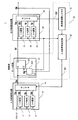
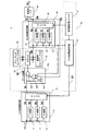
以下、本実施の形態について図面を参照しながら詳細に説明する。図1は、本実施の形態の信号生成回路を示すブロック図である。図1に示すように、本実施の形態の信号生成回路1は、入力段遅延回路10と、出力段遅延回路20と、制御部30を有している。
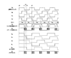
次に、実施の形態2について説明する。実施の形態2は、実施の形態1の信号生成回路1にさらに、カウンタ、周期用コンペアレジスタ、及びデューティ用コンペアレジスタを有する。また、出力段遅延回路20及びデューティ用コンペアレジスタから出力される信号が入力される反転用フリップフロップ(以下、反転用F/Fという。)を有する。実施の形態2にかかる信号生成回路2では、出力信号のデューティ比を基準クロックの周期よりも短い単位で制御する場合に、カウンタのクロックを一定期間延伸する期間を設けるものである。以下に、実施の形態2にかかる信号生成回路2について詳細に説明する。
10 入力段遅延回路
11、12、13、21、22、23 遅延素子
14、24、セレクタ
20 出力段遅延回路
30 制御部
31 周波数調整レジスタ
32 入力段遅延設定部
33、33b ゲート回路
331 ラッチ回路
332 一致検出部
333 ANDゲート
334 NORゲート
335 ORゲート
34 カウンタ
35 周期用コンペアレジスタ
36 デューティ用コンペアレジスタ
40 反転用F/F
Claims (8)
- 基準クロックを出力する状態と、前記基準クロックに前記基準クロックの1周期より短い第1時間の遅延を持たせた信号を出力する状態と、を切り換え可能な入力段遅延回路と、
前記入力段遅延回路の出力が変化した時点から前記入力段遅延回路の出力を前記基準クロックの1周期より短い第2時間保持するゲート回路を有し、前記ゲート回路の出力に対応する信号を出力する制御部と、
前記制御部の出力信号に前記第2時間の遅延を持たせた信号を出力する出力段遅延回路と、を備え、
前記ゲート回路は、前記入力段遅延回路の出力と、前記制御部の出力と、前記出力段遅延回路の出力とが不一致の場合に、前記入力段遅延回路の出力を前記第2時間保持し、
前記制御部は、当該制御部の出力信号の変化に応答して、前記入力段遅延回路の出力状態の切り換えを行う選択信号を出力する入力段遅延回路設定部を有する信号生成回路。 - 請求項1に記載の信号生成回路であって、
前記入力段遅延回路は、前記第1時間の遅延を持たせることができる遅延素子を備え、
前記出力段遅延回路は、前記第2時間の遅延を持たせることができる遅延素子を備える信号生成回路。 - 請求項2に記載の信号生成回路であって、
前記第2時間が、前記基準クロックの1周期に対して、m/n(m、nは自然数、かつ、m<n、かつ、既約分数)時間に相当する場合、前記入力段遅延回路及び前記出力段遅延回路は、それぞれ、1/n、2/n、・・・、(n−2)/n、(n−1)/n時間の遅延を持たせることができる(n−1)個の遅延素子を備える信号生成回路。 - 請求項3に記載の信号生成回路であって、
前記出力段遅延回路は、前記(n−1)個の遅延素子の中から前記m/n時間の遅延を持たせることができる遅延素子を選択する信号生成回路。 - 請求項4に記載の信号生成回路であって、
前記出力段遅延回路の遅延時間を設定する調整値を出力する周波数調整レジスタをさらに備え、
前記入力段遅延回路設定部は、前記入力段遅延回路が当初前記基準クロックを出力する状態を選択した後初めて前記出力状態の切り換えを行うときに、前記調整値に応じて前記出力段遅延回路にて選択されている遅延素子と同等の遅延時間を持たせることが可能な遅延素子を選択する前記選択信号を出力する信号生成回路。 - 請求項1乃至5の何れか1項に記載の信号生成回路であって、
前記ゲート回路は、前記入力段遅延回路の出力と、前記制御部の出力と、前記出力段遅延回路の出力とが全て一致する場合に、前記入力段遅延回路の出力を保持せず、そのまま出力する信号生成回路。 - 請求項1乃至6の何れか1項に記載の信号生成回路であって、
前記制御部は、
前記ゲート回路から出力されるパルス数をカウントするカウンタと、
前記カウンタのカウント値と比較される周期設定値を格納する周期用コンペアレジスタと、を有し、
前記制御部は、前記カウント値と前記周期設定値との比較結果を前記ゲート回路の出力に対応する信号として出力する信号生成回路。 - 請求項7に記載の信号生成回路であって、
前記制御部は、
前記カウンタのカウント値と比較されるデューティ設定値を格納するデューティ用コンペアレジスタを有し、
前記信号生成回路は、
前記カウント値と前記デューティ設定値との比較結果と、前記出力段遅延回路の出力と、を入力する反転用フリップフロップを備え、
前記反転用フリップフロップは、前記カウント値と前記デューティ設定値との比較結果の変化及び前記出力段遅延回路の出力の変化に応答して、出力信号の論理レベルを変更する信号生成回路。
Priority Applications (4)
| Application Number | Priority Date | Filing Date | Title |
|---|---|---|---|
| JP2007314896A JP5154901B2 (ja) | 2007-12-05 | 2007-12-05 | 信号生成回路 |
| US12/292,618 US7696803B2 (en) | 2007-12-05 | 2008-11-21 | Signal generating circuit |
| KR1020080122278A KR101074302B1 (ko) | 2007-12-05 | 2008-12-04 | 신호 생성 회로 |
| DE102008060426A DE102008060426B4 (de) | 2007-12-05 | 2008-12-04 | Signalerzeugerschaltung |
Applications Claiming Priority (1)
| Application Number | Priority Date | Filing Date | Title |
|---|---|---|---|
| JP2007314896A JP5154901B2 (ja) | 2007-12-05 | 2007-12-05 | 信号生成回路 |
Publications (2)
| Publication Number | Publication Date |
|---|---|
| JP2009141596A JP2009141596A (ja) | 2009-06-25 |
| JP5154901B2 true JP5154901B2 (ja) | 2013-02-27 |
Family
ID=40680287
Family Applications (1)
| Application Number | Title | Priority Date | Filing Date |
|---|---|---|---|
| JP2007314896A Expired - Fee Related JP5154901B2 (ja) | 2007-12-05 | 2007-12-05 | 信号生成回路 |
Country Status (4)
| Country | Link |
|---|---|
| US (1) | US7696803B2 (ja) |
| JP (1) | JP5154901B2 (ja) |
| KR (1) | KR101074302B1 (ja) |
| DE (1) | DE102008060426B4 (ja) |
Families Citing this family (1)
| Publication number | Priority date | Publication date | Assignee | Title |
|---|---|---|---|---|
| CN105099435B (zh) * | 2015-08-27 | 2018-04-10 | 深圳市华星光电技术有限公司 | 电平转换电路及其电平转换方法 |
Family Cites Families (9)
| Publication number | Priority date | Publication date | Assignee | Title |
|---|---|---|---|---|
| JPH05167404A (ja) * | 1991-12-12 | 1993-07-02 | Matsushita Electric Ind Co Ltd | 発振制御装置 |
| JPH05191235A (ja) * | 1992-01-10 | 1993-07-30 | Nec Corp | タイミング信号断検出装置 |
| JP3209720B2 (ja) * | 1997-08-04 | 2001-09-17 | 松下電器産業株式会社 | 複数伝送線路間の遅延時間の調整装置及び調整方法 |
| JP3817958B2 (ja) | 1999-03-16 | 2006-09-06 | セイコーエプソン株式会社 | Pwm制御回路、マイクロコンピュータ、及び電子機器 |
| JP2001075671A (ja) * | 1999-09-08 | 2001-03-23 | Nec Corp | 位相補償回路 |
| JP2003023343A (ja) * | 2001-07-10 | 2003-01-24 | Mitsubishi Electric Corp | 遅延信号生成回路 |
| US7453301B1 (en) * | 2005-08-05 | 2008-11-18 | Xilinx, Inc. | Method of and circuit for phase shifting a clock signal |
| US7224199B1 (en) * | 2005-11-04 | 2007-05-29 | National Semiconductor Corporation | Circuit and method for digital delay and circuits incorporating the same |
| US20070210846A1 (en) * | 2006-03-10 | 2007-09-13 | Himax Technologies, Inc. | Inverter gate delay line with delay adjustment circuit |
-
2007
- 2007-12-05 JP JP2007314896A patent/JP5154901B2/ja not_active Expired - Fee Related
-
2008
- 2008-11-21 US US12/292,618 patent/US7696803B2/en active Active
- 2008-12-04 KR KR1020080122278A patent/KR101074302B1/ko not_active Expired - Fee Related
- 2008-12-04 DE DE102008060426A patent/DE102008060426B4/de not_active Expired - Fee Related
Also Published As
| Publication number | Publication date |
|---|---|
| KR101074302B1 (ko) | 2011-10-17 |
| DE102008060426B4 (de) | 2013-02-07 |
| US20090146710A1 (en) | 2009-06-11 |
| DE102008060426A1 (de) | 2009-06-18 |
| US7696803B2 (en) | 2010-04-13 |
| JP2009141596A (ja) | 2009-06-25 |
| KR20090059049A (ko) | 2009-06-10 |
Similar Documents
| Publication | Publication Date | Title |
|---|---|---|
| JP6320705B2 (ja) | 初期位相可変リング発振器 | |
| US20090238017A1 (en) | Digital dll circuit | |
| JP5885977B2 (ja) | Pwm信号出力回路とpwm信号出力制御方法およびプログラム | |
| JP4704260B2 (ja) | Pwm出力回路 | |
| JP6990313B2 (ja) | 半導体集積回路 | |
| JP4943729B2 (ja) | 半導体集積回路装置とac特性測定システム | |
| JP5154901B2 (ja) | 信号生成回路 | |
| US8094698B2 (en) | Method for generating a spread spectrum clock and apparatus thereof | |
| US8729943B2 (en) | Phase interpolating apparatus and method | |
| US20100201409A1 (en) | Frequency Divider Circuit | |
| JP2007047160A (ja) | 調節可能な時間アキュムレータ | |
| JP4434277B2 (ja) | クロック生成回路およびその使用方法 | |
| JP2006303863A (ja) | パルス信号生成装置 | |
| CN118041345A (zh) | 分频系数动态可配的任意整数分频器 | |
| JP2000049595A (ja) | Dll回路 | |
| KR100594315B1 (ko) | 다중 펄스 생성 장치 | |
| JP7220401B2 (ja) | パルス幅変調回路 | |
| JP2006525750A (ja) | 波形グリッチ防止方法 | |
| JP6498031B2 (ja) | 分周回路、分周回路の制御方法およびアナログ電子時計 | |
| JP4908056B2 (ja) | 半導体装置および半導体装置のテスト実行方法 | |
| JP5092475B2 (ja) | 遅延信号発生回路 | |
| JP2012052913A (ja) | 試験装置および信号発生装置 | |
| JP4838060B2 (ja) | アナログ波形発生装置 | |
| JP2015162866A (ja) | クロック遅延生成回路 | |
| CN103580657B (zh) | 相位内插装置以及相位内插方法 |
Legal Events
| Date | Code | Title | Description |
|---|---|---|---|
| A621 | Written request for application examination |
Free format text: JAPANESE INTERMEDIATE CODE: A621 Effective date: 20100806 |
|
| A977 | Report on retrieval |
Free format text: JAPANESE INTERMEDIATE CODE: A971007 Effective date: 20120217 |
|
| A131 | Notification of reasons for refusal |
Free format text: JAPANESE INTERMEDIATE CODE: A131 Effective date: 20120313 |
|
| A521 | Request for written amendment filed |
Free format text: JAPANESE INTERMEDIATE CODE: A523 Effective date: 20120427 |
|
| TRDD | Decision of grant or rejection written | ||
| A01 | Written decision to grant a patent or to grant a registration (utility model) |
Free format text: JAPANESE INTERMEDIATE CODE: A01 Effective date: 20121127 |
|
| A61 | First payment of annual fees (during grant procedure) |
Free format text: JAPANESE INTERMEDIATE CODE: A61 Effective date: 20121206 |
|
| FPAY | Renewal fee payment (event date is renewal date of database) |
Free format text: PAYMENT UNTIL: 20151214 Year of fee payment: 3 |
|
| R150 | Certificate of patent or registration of utility model |
Ref document number: 5154901 Country of ref document: JP Free format text: JAPANESE INTERMEDIATE CODE: R150 Free format text: JAPANESE INTERMEDIATE CODE: R150 |
|
| S531 | Written request for registration of change of domicile |
Free format text: JAPANESE INTERMEDIATE CODE: R313531 |
|
| R350 | Written notification of registration of transfer |
Free format text: JAPANESE INTERMEDIATE CODE: R350 |
|
| LAPS | Cancellation because of no payment of annual fees |