JP5154901B2 - Signal generation circuit - Google Patents
Signal generation circuit Download PDFInfo
- Publication number
- JP5154901B2 JP5154901B2 JP2007314896A JP2007314896A JP5154901B2 JP 5154901 B2 JP5154901 B2 JP 5154901B2 JP 2007314896 A JP2007314896 A JP 2007314896A JP 2007314896 A JP2007314896 A JP 2007314896A JP 5154901 B2 JP5154901 B2 JP 5154901B2
- Authority
- JP
- Japan
- Prior art keywords
- output
- circuit
- signal
- stage delay
- delay
- Prior art date
- Legal status (The legal status is an assumption and is not a legal conclusion. Google has not performed a legal analysis and makes no representation as to the accuracy of the status listed.)
- Expired - Fee Related
Links
Images

Classifications
-
- H—ELECTRICITY
- H03—ELECTRONIC CIRCUITRY
- H03K—PULSE TECHNIQUE
- H03K5/00—Manipulating of pulses not covered by one of the other main groups of this subclass
- H03K5/156—Arrangements in which a continuous pulse train is transformed into a train having a desired pattern
-
- H—ELECTRICITY
- H03—ELECTRONIC CIRCUITRY
- H03M—CODING; DECODING; CODE CONVERSION IN GENERAL
- H03M1/00—Analogue/digital conversion; Digital/analogue conversion
- H03M1/66—Digital/analogue converters
- H03M1/82—Digital/analogue converters with intermediate conversion to time interval
-
- H—ELECTRICITY
- H03—ELECTRONIC CIRCUITRY
- H03L—AUTOMATIC CONTROL, STARTING, SYNCHRONISATION OR STABILISATION OF GENERATORS OF ELECTRONIC OSCILLATIONS OR PULSES
- H03L7/00—Automatic control of frequency or phase; Synchronisation
-
- H—ELECTRICITY
- H03—ELECTRONIC CIRCUITRY
- H03M—CODING; DECODING; CODE CONVERSION IN GENERAL
- H03M5/00—Conversion of the form of the representation of individual digits
- H03M5/02—Conversion to or from representation by pulses
- H03M5/04—Conversion to or from representation by pulses the pulses having two levels
- H03M5/06—Code representation, e.g. transition, for a given bit cell depending only on the information in that bit cell
- H03M5/08—Code representation by pulse width
Landscapes
- Engineering & Computer Science (AREA)
- Theoretical Computer Science (AREA)
- Physics & Mathematics (AREA)
- Nonlinear Science (AREA)
- Pulse Circuits (AREA)
- Stabilization Of Oscillater, Synchronisation, Frequency Synthesizers (AREA)
Description
本発明は、出力信号のLレベル期間、Hレベル期間を制御する信号生成回路に関する。 The present invention relates to a signal generation circuit that controls an L level period and an H level period of an output signal.
近年の電子機器の高速化に応じて、パルスの遷移するタイミングをより高精度に制御することが重要となっている。特許文献1には、遅延回路を用いて立ち上がりエッジを遅延させるPWM制御回路が開示されている。PWM制御回路は、立ち上がりエッジを遅延させることによりデューティ比を変えた信号を出力している。しかしながら、特許文献1に記載のPWM制御回路は、出力する信号の周期については全く考慮されていない。一方、特許文献2に、周期を延伸させた信号を出力する発振制御装置が記載されている。特許文献2に記載の発振制御装置には、発振器で生成した基準クロックを複数の遅延回路で遅延させ、カウンタの値に基づいて複数の遅延回路の出力から任意の出力を選択し、クロックのパルス幅を延伸させる発振制御装置が開示されている。
しかしながら、特許文献2に記載の発振制御装置では、パルス幅を延伸させた信号又はパルス幅を延伸させない信号が出力されるのみである。このため、周期の延伸を考慮した複数種類の信号を出力することが困難であるという問題点がある。
However, the oscillation control device described in
本発明に係る信号生成回路は、基準クロックを出力する状態と、前記基準クロックに前記基準クロックの1周期より短い第1時間の遅延を持たせた信号を出力する状態と、を切り換え可能な入力段遅延回路と、前記入力段遅延回路の出力が変化した時点から前記入力段遅延回路の出力を前記基準クロックの1周期より短い第2時間保持するゲート回路を有し、前記ゲート回路の出力に対応する信号を出力する制御部と、前記制御部の出力信号に前記第2時間の遅延を持たせた信号を出力する出力段遅延回路と、を備え、前記入力段遅延回路は、前記制御部の出力信号の変化に応答して出力状態の切り換えを行うものである。 The signal generation circuit according to the present invention can switch between a state of outputting a reference clock and a state of outputting a signal having a delay of a first time shorter than one cycle of the reference clock. A stage delay circuit, and a gate circuit that holds the output of the input stage delay circuit for a second time shorter than one cycle of the reference clock from the time when the output of the input stage delay circuit changes, the output of the gate circuit A control unit that outputs a corresponding signal; and an output stage delay circuit that outputs a signal obtained by adding a delay of the second time to the output signal of the control unit, wherein the input stage delay circuit includes the control unit The output state is switched in response to the change in the output signal.
制御部により、入力段遅延回路の出力が変化した時点から、当該入力段遅延回路の出力を基準クロックの1周期より短い第2時間保持し、当該制御部の出力信号の変化に応答して入力段遅延回路の出力状態の切り換えが行われるため、出力段遅延回路から第2時間の遅延を持たせた信号を出力することができる。 From the time when the output of the input stage delay circuit changes by the control unit, the output of the input stage delay circuit is held for a second time shorter than one cycle of the reference clock, and input in response to the change of the output signal of the control unit Since the output state of the stage delay circuit is switched, a signal having a second time delay can be output from the output stage delay circuit.
本発明によれば、基準クロックの周期より細かい周期で制御された複数の出力信号を出力する信号生成回路を提供することができる。 According to the present invention, it is possible to provide a signal generation circuit that outputs a plurality of output signals controlled at a period finer than the period of the reference clock.
実施の形態1.
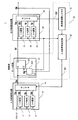
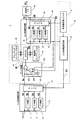
以下、本実施の形態について図面を参照しながら詳細に説明する。図1は、本実施の形態の信号生成回路を示すブロック図である。図1に示すように、本実施の形態の信号生成回路1は、入力段遅延回路10と、出力段遅延回路20と、制御部30を有している。
Hereinafter, the present embodiment will be described in detail with reference to the drawings. FIG. 1 is a block diagram showing a signal generation circuit according to the present embodiment. As shown in FIG. 1, the
入力段遅延回路10は、複数の遅延素子11乃至13と、セレクタ14とを有する。複数の遅延素子11乃至13は、入力された基準クロックを、それぞれ基準クロックに基づいて設定された時間分(第1時間)遅延させて出力する。本実施の形態では、遅延素子11は、基準クロックに1/4周期分の遅延を持たせて出力する。以下、遅延素子12は2/4周期分、遅延素子13は3/4周期分の遅延を持たせて出力する。
The input
入力段遅延回路10のセレクタ14は、後述する入力段遅延選択信号S1に基づいて、基準クロックあるいは遅延素子11乃至13の出力する信号の任意の1つを選択して出力する。このセレクタ14の出力する信号が入力段遅延出力信号Seとして、後述するゲート回路33へ出力される。ここで、セレクタ14では、当初基準クロックを出力する状態を選択する。その後、初めてセレクタ14の選択を切り換える場合、後述する入力段遅延選択信号S1に基づいて任意の1つの遅延素子を選択する。この場合、出力段遅延回路20の後述するセレクタ24に出力される値(選択する遅延素子)と同等の遅延時間を持たせることが可能な遅延素子が選択される。
The
制御部30は、周波数調整レジスタ31と、入力段遅延設定部32と、ゲート回路33とを有している。周波数調整レジスタ31は、出力する信号の周波数に対応する設定を保持するレジスタである。この周波数調整レジスタ31に保持する値は、入力段遅延設定部32、及び後述する出力段遅延回路20のセレクタ24に出力される。
The
入力段遅延設定部32は、入力段遅延回路10内のセレクタ14に対して、基準クロック及び遅延素子11〜13によって基準クロックを遅延させた信号のうちいずれかを選択する入力段遅延選択信号(以下、第1の選択信号という。)S1を出力する。この入力段遅延設定部32は、後述するゲート回路33の出力が遷移するたびに選択する遅延素子を連続的に切り換える。すなわち、ゲート回路33の出力が立ち上がる又は立ち下がったことを受けて選択する遅延素子を順次切り換える回路である。この第1の選択信号S1は、出力段遅延回路20の後述するセレクタ24に出力される値(選択する遅延素子)と同等の遅延時間を持たせることが可能な遅延素子を選択することを示す信号である。
The input stage
ゲート回路33は、入力段遅延回路10の出力する信号(入力段遅延出力信号Se)の出力段遅延回路20への入力を制御する回路である。本実施の形態のゲート回路33は、ラッチ回路331及び一致検出部332を有する。ラッチ回路331は、一致検出部332の出力に基づいて、ラッチ回路331への入力に関わらずその出力値を固定させるか、ラッチ回路331への入力値をそのまま出力するかが決定される。一致検出部332は、ゲート回路33の出力、入力段遅延回路10の出力、出力段遅延回路20の出力の一致、不一致を検出する。一致検出部332はこの3つの入力が一致していない場合には、ラッチ回路331に入力された値に関わらず出力値を固定させる信号を出力する。また、当該3つの入力が一致している場合、ラッチ回路331からは当該ラッチ回路331に入力された値をそのまま出力する。
The
出力段遅延回路20は、周波数調整レジスタ31に設定された値に基づいて、ゲート回路33が出力した信号をそのまま出力、あるいは所定の遅延を持たせて出力する回路である。この出力段遅延回路20は、複数の遅延素子21〜23、セレクタ24を有している。複数の遅延素子21乃至23は、ゲート回路33の出力を、第2時間の遅延を持たせて出力する。本実施の形態では、複数の遅延素子21〜23は、ゲート回路33の出力に、例えばそれぞれ基準クロックの1/4周期分、2/4周期分、3/4周期分の遅延を持たせて出力する。
The output
本実施の形態では、出力段遅延回路20は、当該出力段遅延回路20から基準クロックの1周期に対して、m/n(m、nは自然数、かつ、m<n、かつ、既約分数)時間に相当する時間の遅延を持たせた信号を出力する。この場合、入力段遅延回路10及び出力段遅延回路20は、それぞれ、1/n、2/n、・・・、(n−2)/n、(n−1)/n時間の遅延を持たせることができる(n−1)個の遅延素子を備える。本実施の形態では、n=4であって、入力段遅延回路10及び出力段遅延回路20は、それぞれ遅延素子を3つ有する場合について説明するが、n≧2であれば本発明を適用可能である。
In the present embodiment, the output
出力段遅延回路20内のセレクタ24は、周波数調整レジスタ31に設定された値に基づいて、ゲート回路33の出力あるいは遅延素子21〜23の出力する信号の任意の1つを選択して出力する。すなわち、周波数調整レジスタ31は出力段遅延回路20内のセレクタ24に対して、当該周波数調整レジスタ31に保持され、ゲート回路33の出力あるいは遅延素子21〜23の出力する信号のうちいずれかを選択する出力段遅延選択信号(以下、第2の選択信号という。)S2を出力する。これにより、セレクタ24は、(n−1)個の遅延素子からm/n時間の遅延を持たせることができる遅延素子を選択する。
The
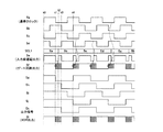
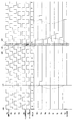
次に、このように構成された信号生成回路1の動作について図2を用いて説明する。図2に、図1に示す信号生成回路1の動作を示すタイミングチャートを示す。すなわち、図2は信号生成回路1における各点での波形を示したタイミングチャートである。また、図2には、各タイミングにおいて、入力段遅延回路10内のセレクタ14が、第1の選択信号S1に基づいてどの遅延素子を出力しているかも併せて示す。図2において、Sa〜Slは、図1のSa〜Slにそれぞれ対応する波形を示す。なお、以下の説明では、出力段遅延回路20は、基準クロックの1周期に対して、1/4時間(この場合、m=1、n=4である)の遅延を持たせた信号を出力する場合について説明する。すなわち、目標とする出力クロックがH区間、L区間共に1/4周期延伸されたもの、つまり、基準クロックの周期を1.25倍にした周期のクロックを出力する例を用いて説明する。
Next, the operation of the
周波数調整レジスタ31には、その出力する信号に対応した値(ここでは、基準クロックの1.25倍周期)を示す値が設定される。この周波数調整レジスタ31に設定された値を出力段遅延選択信号S2として受信する出力段遅延回路20では、セレクタ24の出力する信号を1/4遅延素子の出力Shに固定する。
In the
なお、以下の説明において、クロック入力当初(図2、t0参照)において、ゲート回路出力Sf、出力信号Skは、デフォルトではHレベルに設定されているものとして説明する。 In the following description, it is assumed that the gate circuit output Sf and the output signal Sk are set to H level by default at the beginning of clock input (see t0 in FIG. 2).
基準クロックが入力されると、セレクタ14は、周波数調整レジスタ31に設定されている値に基づいて、入力される基準クロックSaを選択する。そのため、入力段遅延回路10は、時刻t0において、入力段遅延出力信号SeとしてHレベルの信号を出力する。ゲート回路出力SfはHレベルを維持する。
When the reference clock is input, the
その後、時刻t1において、入力されている基準クロックが立ち下がる。セレクタ14は、基準クロックSaを選択しているため、Saの立下りに合わせて、信号Se及びSfが立ち下がる。このとき、出力信号Skとしては、ゲート回路33の出力信号Sfを1/4周期分遅延させた信号(図2、Sh参照)が選択されているため、出力信号SkはHレベルを維持する。ここで、入力段遅延出力信号Se、ゲート回路33の出力Sf、及び出力信号Skに不一致が生じる。このため、一致検出部332の出力が遷移し、ラッチ回路331は入力される信号に関わらず、そのときの出力信号を保持する(図2、Sf、Sl参照)。
Thereafter, the input reference clock falls at time t1. Since the
ゲート回路33の出力Sfが立ち下がって遷移したことにより、入力段遅延設定部32は、セレクタ14に対し、選択する信号を切り換える第1の選択信号S1を出力する。ここで、出力段遅延回路20のセレクタ24では、1/4時間の遅延を持たせた信号を出力する遅延素子21が選択されている。このため、入力段遅延設定部32は、セレクタ14に対し、選択する信号をSbに切り換える第1の選択信号S1を出力する。入力段遅延設定部32からの第1の選択信号S1に基づいて、時刻t2において、1/4遅延素子からの出力Sbを選択する。したがって、入力段遅延出力信号Seも立ち上がりHレベルとなる(図2、t2参照)。このとき、一致検出部332の出力によって、ラッチ回路331は出力が固定された状態となっているため、ゲート回路33の出力Sfは変化せずLレベルを保持する。
When the output Sf of the
その後、時刻t3において、1/4遅延素子11の出力信号Sbの立ち下がりに合わせて、入力段遅延出力信号Seも立ち下がる。入力段遅延出力信号Seが立ち下がることにより、入力段遅延出力信号Se、ゲート回路33の出力Sf、及び出力信号Skのレベルが一致する状態となる。このため、ラッチ回路331は、入力段遅延回路10の出力の保持を解除し、再び入力された信号を出力する状態となる。
Thereafter, at time t3, the input stage delayed output signal Se also falls in accordance with the fall of the output signal Sb of the 1/4
実施の形態1に示す信号生成回路1では、例えば、出力段遅延回路20の遅延素子を1/4周期遅延に固定する。そして、ゲート回路33から出力される信号Sfが遷移すると、入力段遅延回路10の選択する遅延素子を順次切り換える。信号Sfが遷移した後、入力段遅延出力信号Se、ゲート回路33の出力Sf、及び出力信号Skのレベルが一致するまでの間、信号Sfは入力段遅延回路10の出力Seのレベルを保持する。これにより、信号生成回路1から、基準クロックの周期よりも短い単位で周期を延伸させた出力信号Skを出力することができる。
In the
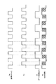
ここで、図3に出力段遅延回路20の遅延素子を2/4周期遅延に固定した場合の動作を示すタイミングチャートを示す。図3では、図2に示す基準クロックSaと、基準クロックを2/4周期分遅延させる遅延素子12からの出力Scと、ゲート回路33の出力Sfと、出力段遅延回路20からの出力信号Skとを示す。図3を用いて、出力段遅延回路20の遅延素子を2/4周期遅延に固定した場合の動作について簡単に説明する。
FIG. 3 is a timing chart showing the operation when the delay element of the output
図3に示すように、入力段遅延回路10では、当初基準クロックを出力する状態を選択する。その後、初めて制御部30のゲート回路33の出力の遷移に応じてセレクタ14の選択を切り換える場合、入力段遅延回路10のセレクタ14は、出力段遅延回路20のセレクタ24に出力される値(選択する遅延素子)と同等の遅延時間を持たせることが可能な遅延素子を選択する第1の選択信号S1を出力する。すなわち、セレクタ14では、2/4周期分遅延させる遅延素子12が選択される。このとき、ゲート回路33の出力Sfは、遅延素子を切り換える際に取り込んだ入力段遅延回路10の出力Seのレベルを、基準クロックの2/4周期分、保持する。その後、遅延素子12からの出力であって、入力段遅延回路10の出力である信号Scと、ゲート回路33の出力Sfと、出力段遅延回路20の出力信号Skとが一致した場合、ラッチ回路331は入力段遅延回路10の出力の保持を解除する。これにより、基準クロックから2/4周期分遅延した信号が出力信号Skとして出力される。
As shown in FIG. 3, the input
出力段遅延回路20の遅延素子を2/4周期遅延に固定した場合、入力段遅延回路10では、基準クロックSaと2/4周期遅延させる遅延素子12が交互に選択される。これに応じて出力段遅延回路20からは、基準クロックの周期よりも短い単位で周期を延伸させた出力信号Skを出力することができる。
When the delay element of the output
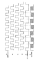
次に、図4に出力段遅延回路20の遅延素子を3/4周期遅延に固定した場合の動作を示すタイミングチャートを示す。図4では、図2に示す基準クロックSaと、各遅延素子から出力される信号Sb〜Sdと、ゲート回路33の出力Sfと、出力段遅延回路20の出力信号Skとを示す。図4を用いて、3/4周期遅延に固定した場合の動作について簡単に説明する。
Next, FIG. 4 shows a timing chart showing an operation when the delay element of the output
図4に示すように、入力段遅延回路10では、当初基準クロックを出力する状態を選択する。その後、ゲート回路33の出力の遷移に応じて、入力段遅延回路10のセレクタ14は、3/4周期分遅延させる遅延素子13を選択する。このとき、ゲート回路33の出力Sfは、遅延素子を切り換える際に取り込んだ入力段遅延回路10の出力Seのレベルを、基準クロックの3/4周期分、保持する。そして、遅延素子13からの出力であって、入力段遅延回路10の出力である信号Sdと、ゲート回路の出力Sfと、出力段遅延回路20の出力信号Skとが一致した場合、ラッチ回路331は入力段遅延回路10の出力の保持を解除する。この後、入力段遅延回路10のセレクタ14は、2/4周期分遅延させる遅延素子12、1/4周期分遅延させる遅延素子11を順に選択する。これにより、基準クロックから3/4周期分延伸した信号が出力信号Skとして出力される。
As shown in FIG. 4, the input
以上から、実施の形態1にかかる信号生成回路1において、入力段遅延回路10及び出力段遅延回路20は、それぞれ基準クロックよりも短い周期の遅延を有する複数の遅延素子を有する。出力段遅延回路20の遅延素子を、例えば1/4周期遅延に固定し、ゲート回路33から出力される信号Sfが遷移すると、入力段遅延回路10の選択する遅延素子を順次切り換える。信号Sfが遷移し、入力段遅延出力信号Seが信号Sfと同じレベルに遷移するまでの間、信号Sfは入力段遅延回路10の出力Seのレベルを保持する。これにより、信号生成回路1から、基準クロックの周期よりも短い単位で周期を延伸させた出力信号Skを出力することができる。また、出力段遅延回路20において、選択する遅延素子を2/4遅延素子、3/4遅延素子に変更することにより、出力信号を1.75倍、2倍延伸させた信号を出力することができる。すなわち、基準クロックの周期より細かい周期で制御された複数の出力信号を出力することができる。また、ラッチ回路331及び一致検出部332からなるゲート回路33、並びに遅延素子11〜13、21〜23を用いた簡単な構成により、基準クロックの周期よりも細かい遅延を持たせた複数の出力信号を生成することができる。
As described above, in the
実施の形態2.
次に、実施の形態2について説明する。実施の形態2は、実施の形態1の信号生成回路1にさらに、カウンタ、周期用コンペアレジスタ、及びデューティ用コンペアレジスタを有する。また、出力段遅延回路20及びデューティ用コンペアレジスタから出力される信号が入力される反転用フリップフロップ(以下、反転用F/Fという。)を有する。実施の形態2にかかる信号生成回路2では、出力信号のデューティ比を基準クロックの周期よりも短い単位で制御する場合に、カウンタのクロックを一定期間延伸する期間を設けるものである。以下に、実施の形態2にかかる信号生成回路2について詳細に説明する。
Next, a second embodiment will be described. In the second embodiment, the
実施の形態2にかかる信号生成回路2の出力信号は、周期用コンペアレジスタに設定されるカウンタのクロック数を出力信号の1周期とする。また、デューティ用コンペアレジスタに設定されるカウンタのクロック数とカウンタのカウントが一致すると、出力信号がHレベルからLレベルに遷移する。以下、実施の形態2の信号生成回路2について図5を用いて詳細に説明する。図5は、実施の形態2にかかる信号生成回路2を示すブロック図である。図5に示す実施の形態2にかかる信号生成回路2において、図1に示す実施の形態1と同一構成要素には同一の符号を付し、その詳細な説明は省略する。
In the output signal of the
図5に示すように、本実施の形態にかかる信号生成回路2は、制御部30に、カウンタ34、周期用コンペアレジスタ35、及びデューティ用コンペアレジスタ36をさらに有し、出力段遅延回路20の出力側に反転用F/F40を有する。
As shown in FIG. 5, the
カウンタ34は、ゲート回路33bから出力される信号Sfのパルスをカウントする。
The counter 34 counts pulses of the signal Sf output from the
周期用コンペアレジスタ35は、目標とする出力クロックの1周期分のクロック数(以下、周期設定値という。)(例えば8クロック)が設定される。また、カウンタ34と周期用コンペアレジスタ35の間には図示せぬ比較部を有している。この比較部は、周期設定値と、カウンタ34のクロック数を比較し、これらのクロック数が一致しない場合は、Lレベルの信号Smを出力する。一方、周期設定値とカウンタ34のクロック数が一致する場合にHレベルの信号Smを出力する。この周期用コンペアレジスタ35と図示せぬ比較部との比較結果に応じた信号が、ゲート回路33bの出力に対応する信号として制御部30から出力される。
In the cycle compare
デューティ用コンペアレジスタ36は、信号生成回路2から出力される出力信号Soが例えばH区間からL区間に遷移するタイミングのクロック数(以下、デューティ設定値という。)(例えば3クロック)が設定される。また、カウンタ34とデューティ用コンペアレジスタ36の間には図示せぬ比較部を有している。この比較部は、デューティ設定値と、カウンタ34のクロック数を比較し、これらのクロック数が一致しない場合は、Lレベルの信号Snを出力する。一方、デューティ設定値とカウンタ34のクロック数が一致する場合にHレベルの信号Snを出力する。
In the duty compare
反転用F/F40は、カウンタ34とデューティ用コンペアレジスタ36の間に形成されている図示せぬ比較部から出力される信号Snが遷移する場合に、出力信号Soを遷移させる。また、出力段遅延回路20から出力される信号Skが遷移する場合に、出力信号Soを遷移させる。すなわち、反転用F/F40は、信号Sn及び出力段遅延回路20の出力Skに応答して、出力信号Soの論理レベルを変更する。
The inversion F /
また、ゲート回路33bは、例えば、ANDゲート333、NORゲート334、及びORゲート335を有する。このゲート回路33bは、入力段遅延回路10内のセレクタ14が第1の選択信号S1に基づいて出力する信号を切り換える場合に、カウンタ34がカウントアップしないように、ゲート回路33bの出力信号Sfを一定期間延伸させる。
The
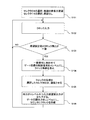
次に、このように構成された信号生成回路2の動作について、図6及び図7を用いて以下に説明する。図6は、信号生成回路2における各点での波形を示したタイミングチャートである。図6において、Sa〜Sk、Sm〜Soは、図5のSa〜Sk、Sm〜Soに対応する波形を示す。図7は、図6に示す信号生成回路2の動作を示すフローチャートである。以下の説明では、目標とする出力クロックのデューティ比を1/4周期単位で制御する場合の例を用いて説明する。
Next, the operation of the
なお、以下の説明では、クロック入力当初(図6、t00参照)において、ゲート回路出力Sfは、デフォルトではHレベルに設定されているものとして説明する。 In the following description, it is assumed that the gate circuit output Sf is set to H level by default at the beginning of clock input (see t00 in FIG. 6).
まず、周波数調整レジスタ31には、その出力する信号に対応した値(ここでは、出力信号を基準クロックの1/4周期単位で制御する)を示す値が設定される。この周波数調整レジスタ31に設定された値を第2の選択信号S2として受信した出力段遅延回路20では、セレクタ24の出力する信号を1/4遅延素子の出力Shに固定する。また、セレクタ14では、当初基準クロックを出力する状態が選択される(図7、ステップS101)。
First, the
基準クロックが入力されると(図7、ステップS102)、セレクタ14は、周波数調整レジスタ31に設定されている値に基づいて入力される基準クロックSaを選択する。そのため、入力段遅延回路10は、時刻t00において、Hレベルの信号を出力する。このとき、反転用F/F40から出力される出力信号oも立ち上がり、Hレベルの信号を出力する。
When the reference clock is input (FIG. 7, step S102), the
その後、時刻t11において、カウンタ34が、入力される基準クロックの4クロック目の立ち上がりをカウントする。このとき、デューティ設定値とカウンタ34のクロック数が一致する。これにより、デューティ用コンペアレジスタ36とカウンタ34の間にある図示せぬ比較部から出力される信号Snが立ち上がる(図6、Sn参照)。信号Snが立ち上がると、反転用F/F40は、出力信号を反転させる。すなわち、出力信号Soが立ち下がる。
Thereafter, at time t11, the
そして、時刻t22において、基準クロックが立ち上がる。セレクタ14は、基準クロックSaを選択しているため、Saの立ち上がりに合わせて、信号Se及びSfが立ち上がる。これにより、カウンタ34が、入力される基準クロックの8クロック目の立ち上がりをカウントする。このとき、周期設定値とカウンタ34のクロック数が一致する(図7、ステップS103)。これにより、周期用コンペアレジスタ35とカウンタ34の間にある図示せぬ比較部から出力される信号Smが立ち上がる(図6、Sm参照)。このとき、出力段遅延回路20の出力信号Skとしては、信号Smを1/4周期分遅延させた信号Sh(図6、Sh、Sk参照)が選択されているため、出力信号SkはLレベルを維持する。これにより、反転用F/F40から出力される信号SoもLレベルを維持する。なお、図7のステップS103において周期設定値とカウンタ34のクロック数が一致しない場合、再度ステップS102に戻る。
At time t22, the reference clock rises. Since the
信号Smが遷移したことにより、入力段遅延設定部32は、セレクタ14に対し、選択する信号をSbに切り換える信号を出力する。すなわち、時刻t33において、入力段遅延設定部32からの第1の選択信号S1に基づいて、1/4遅延素子からの出力Sbを選択する。したがって、入力段遅延出力信号Seが立ち下がりLレベルとなる(図6、Se参照)。このとき、ゲート回路33bは、カウンタ34をカウントアップしないように出力が固定された状態となっているため、ゲート回路33bの出力Sfは変化せずHレベルを維持する(図6のSf参照、図7のステップS104参照)。すなわち、入力段遅延回路10の出力のレベルが保持される。このとき、出力信号SkはLレベルを維持し、信号SoもLレベルを維持する。
Due to the transition of the signal Sm, the input stage
その後、時刻t44において、1/4遅延素子11の出力信号が立ち上がることに合わせて、入力段遅延出力信号Seが立ち上がる(図7、ステップS105)。このとき、出力段遅延回路20の出力信号Skが信号Smより1/4周期遅延して立ち上がる。これにより、反転用F/F40に入力される信号Skが遷移するため、反転用F/F40は出力信号Soを遷移させる。このとき、入力段遅延回路10の出力Seと、制御部30の出力Smと、出力信号Skのレベルが一致し、入力段遅延回路10の出力の保持が解除される。これにより、出力信号Soの2周期目が始まり、ゲート回路33bは再び入力される信号を出力する状態となる(図6、t44におけるSf参照)。そして、出力信号SoがHレベルであって入力段遅延回路10の出力Seが立ち下がる。また、ゲート回路33bの出力SfがLレベルになり、カウンタ34にクロックが供給される(図7、ステップS106)。その後、再びステップS102に戻り、上述の動作を繰り返すことにより、デューティ比が1/4周期単位で制御された信号が出力される。
Thereafter, at time t44, the input stage delay output signal Se rises in accordance with the rise of the output signal of the 1/4 delay element 11 (FIG. 7, step S105). At this time, the output signal Sk of the output
以上から、実施の形態2にかかる信号生成回路2において、入力段遅延回路10及び出力段遅延回路20は、それぞれ基準クロックよりも短い周期の遅延を有する複数の遅延素子を有する。そして、出力段遅延回路20の遅延素子を1/4周期遅延に固定し、カウンタ34と周期用コンペアレジスタ35の間にある比較部から出力される信号Smが遷移する場合に、入力段遅延回路10の選択する遅延素子を順次切り換える。このとき、入力段遅延回路10の出力は、出力段遅延回路20で選択した遅延期間分、保持される。これにより、信号生成回路2から基準クロックの周期よりも細かい単位で出力信号のデューティ比を制御した信号を出力することができる。また、出力段遅延回路20において選択する遅延素子を2/4遅延素子、3/4遅延素子に変更することにより、出力信号のデューティ比を2/4周期単位、3/4周期単位で制御することができる。出力段遅延回路20において選択する遅延素子を2/4遅延素子22、3/4遅延素子23に変更した場合の信号生成回路2の動作については後述する。
As described above, in the
また、出力信号のデューティ比を基準クロックの周期よりも短い単位で制御する場合に、カウンタのクロックを一定期間延伸する期間を設ける。すなわち、出力信号Soが1周期目から2周期目に切り替わる際に、入力段遅延回路10からの出力信号SeがSaからSbに切り替わり、次に出力信号Soが立ち上がるまで、カウンタ34がクロック数をカウントアップしないようにゲート回路33bの出力信号Sfは入力段遅延回路10の出力Seのレベルを保持する。これにより、出力信号Soのデューティ比を基準クロックの周期よりも短い単位で制御する場合に、制御した期間分のカウンタ34のカウント期間が延伸する。このため、出力信号Soをカウンタ34が1クロックカウントすることを待つことなく出力することができる。このため、信号生成回路2の動作速度を向上させることができる。
Further, when the duty ratio of the output signal is controlled in units shorter than the cycle of the reference clock, a period for extending the counter clock for a certain period is provided. That is, when the output signal So is switched from the first cycle to the second cycle, the
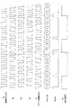
ここで、図8に出力クロックのデューティ比を2/4周期単位で制御する場合の動作を示すタイミングチャートを示す。また、図9に出力クロックのデューティ比を3/4周期単位で制御する場合の動作を示すタイミングチャートを示す。図8及び図9では、図6に示す信号Smと信号Snとを併せて記載する。 FIG. 8 is a timing chart showing the operation when the duty ratio of the output clock is controlled in units of 2/4 cycles. FIG. 9 is a timing chart showing the operation when the duty ratio of the output clock is controlled in units of 3/4 cycles. 8 and 9, the signal Sm and the signal Sn shown in FIG. 6 are described together.
まず、デューティ比を2/4周期単位で制御する場合の動作について簡単に説明する。図8に示すように、例えば出力クロックのデューティ比を2/4周期単位で制御する場合、出力段遅延回路20の遅延素子を2/4周期遅延に固定する。入力段遅延回路10の出力は当初基準クロックが出力される。そして、例えばカウンタ34が、基準クロックの4クロック目の立ち上がりをカウントし、信号Snが立ち上がる。これにより、出力信号Soが立ち下がる。次に、カウンタ34が、入力される基準クロックの8クロック目の立ち上がりをカウントする。これにより、制御部30の出力Smが立ち上がり、入力段遅延回路10のセレクタ14は選択する信号をScに切り換える。このとき、ゲート回路33bの出力Sfは、入力段遅延回路10の出力Se(図示せず)のレベルを保持する。次に2/4遅延素子11の出力信号Scが立ち上がることに合わせて、入力段遅延回路10の出力信号Seが立ち上がる。そして、出力段遅延回路20の出力信号Skが信号Smより2/4周期遅延して立ち上がる。これにより、反転用F/F40に入力される信号Skが遷移し、入力段遅延回路10の出力Seの保持が解除される。そして、反転用F/F40は出力信号Soを遷移させ、2周期目が始まる。
First, the operation when the duty ratio is controlled in units of 2/4 cycles will be briefly described. As shown in FIG. 8, for example, when the duty ratio of the output clock is controlled in units of 2/4 cycles, the delay element of the output
このように、カウンタ34が周期用コンペアレジスタ35に格納されたクロック数をカウントすると、出力信号Soが立ち下がり、デューティ用コンペアレジスタ36に格納されたクロック数をカウントすると、選択した遅延素子の期間分、カウンタ34のクロックが延伸する。また、図9に示すデューティ比を3/4周期単位で制御する場合は、カウンタ34のカウントを3/4周期延伸する。これにより、出力信号Soのデューティ比を基準クロックの周期よりも短い単位で制御することができる。
Thus, when the counter 34 counts the number of clocks stored in the period compare
以上から、実施の形態2にかかる信号生成回路2において、例えば、出力段遅延回路20の遅延素子を1/4周期遅延に固定する。そして、カウンタ34と周期用コンペアレジスタ35の間にある比較部から出力される信号Smが遷移する場合に、入力段遅延回路10の選択する遅延素子を順次切り換える。このとき、入力段遅延回路10の出力Seが、出力段遅延回路20で選択した遅延期間分、保持される。これにより、信号生成回路2から基準クロックの周期よりも細かい単位で出力信号のデューティ比を制御した信号を出力することができる。
From the above, in the
なお、本発明は上述した実施の形態のみに限定されるものではなく、本発明の要旨を逸脱しない範囲において種々の変更が可能であることは勿論である。例えば、本実施の形態では、入力段遅延回路10及び出力段遅延回路20はそれぞれ3つの遅延素子を有することとしたが、出力信号の制御に応じて遅延素子の数を増減させることが可能である。
It should be noted that the present invention is not limited to the above-described embodiments, and various modifications can be made without departing from the scope of the present invention. For example, in this embodiment, the input
1、2 信号生成回路
10 入力段遅延回路
11、12、13、21、22、23 遅延素子
14、24、セレクタ
20 出力段遅延回路
30 制御部
31 周波数調整レジスタ
32 入力段遅延設定部
33、33b ゲート回路
331 ラッチ回路
332 一致検出部
333 ANDゲート
334 NORゲート
335 ORゲート
34 カウンタ
35 周期用コンペアレジスタ
36 デューティ用コンペアレジスタ
40 反転用F/F
DESCRIPTION OF
Claims (8)
前記入力段遅延回路の出力が変化した時点から前記入力段遅延回路の出力を前記基準クロックの1周期より短い第2時間保持するゲート回路を有し、前記ゲート回路の出力に対応する信号を出力する制御部と、
前記制御部の出力信号に前記第2時間の遅延を持たせた信号を出力する出力段遅延回路と、を備え、
前記ゲート回路は、前記入力段遅延回路の出力と、前記制御部の出力と、前記出力段遅延回路の出力とが不一致の場合に、前記入力段遅延回路の出力を前記第2時間保持し、
前記制御部は、当該制御部の出力信号の変化に応答して、前記入力段遅延回路の出力状態の切り換えを行う選択信号を出力する入力段遅延回路設定部を有する信号生成回路。 An input stage delay circuit capable of switching between a state of outputting a reference clock and a state of outputting a signal having a delay of a first time shorter than one cycle of the reference clock to the reference clock;
A gate circuit that holds the output of the input stage delay circuit for a second time shorter than one cycle of the reference clock from the time when the output of the input stage delay circuit changes, and outputs a signal corresponding to the output of the gate circuit; A control unit,
An output stage delay circuit for outputting a signal obtained by delaying the output signal of the control unit by the second time,
The gate circuit holds the output of the input stage delay circuit for the second time when the output of the input stage delay circuit, the output of the control unit, and the output of the output stage delay circuit do not match;
The signal generation circuit includes an input stage delay circuit setting unit that outputs a selection signal for switching an output state of the input stage delay circuit in response to a change in an output signal of the control unit .
前記入力段遅延回路は、前記第1時間の遅延を持たせることができる遅延素子を備え、
前記出力段遅延回路は、前記第2時間の遅延を持たせることができる遅延素子を備える信号生成回路。 The signal generation circuit according to claim 1,
The input stage delay circuit includes a delay element that can have a delay of the first time,
The output stage delay circuit is a signal generation circuit including a delay element capable of giving a delay of the second time.
前記第2時間が、前記基準クロックの1周期に対して、m/n(m、nは自然数、かつ、m<n、かつ、既約分数)時間に相当する場合、前記入力段遅延回路及び前記出力段遅延回路は、それぞれ、1/n、2/n、・・・、(n−2)/n、(n−1)/n時間の遅延を持たせることができる(n−1)個の遅延素子を備える信号生成回路。 The signal generation circuit according to claim 2,
When the second time corresponds to m / n (m, n is a natural number and m <n and an irreducible fraction) time with respect to one cycle of the reference clock, the input stage delay circuit and The output stage delay circuits can have delays of 1 / n, 2 / n, ..., (n-2) / n, (n-1) / n hours, respectively (n-1). A signal generation circuit comprising delay elements.
前記出力段遅延回路は、前記(n−1)個の遅延素子の中から前記m/n時間の遅延を持たせることができる遅延素子を選択する信号生成回路。 The signal generation circuit according to claim 3,
The output stage delay circuit is a signal generation circuit that selects a delay element that can have a delay of the m / n time from the (n-1) delay elements.
前記出力段遅延回路の遅延時間を設定する調整値を出力する周波数調整レジスタをさらに備え、
前記入力段遅延回路設定部は、前記入力段遅延回路が当初前記基準クロックを出力する状態を選択した後初めて前記出力状態の切り換えを行うときに、前記調整値に応じて前記出力段遅延回路にて選択されている遅延素子と同等の遅延時間を持たせることが可能な遅延素子を選択する前記選択信号を出力する信号生成回路。 The signal generation circuit according to claim 4,
A frequency adjustment register that outputs an adjustment value for setting a delay time of the output stage delay circuit;
Wherein the input stage delay circuit setting section when performing the first switching of the output state after the input stage delay circuit selects the state of outputting the original the reference clock, the output stage delay circuit in response to the adjustment value A signal generation circuit that outputs the selection signal for selecting a delay element that can have a delay time equivalent to that of the delay element selected in (1).
前記ゲート回路は、前記入力段遅延回路の出力と、前記制御部の出力と、前記出力段遅延回路の出力とが全て一致する場合に、前記入力段遅延回路の出力を保持せず、そのまま出力する信号生成回路。 A signal generation circuit according to any one of claims 1 to 5,
When the output of the input stage delay circuit, the output of the control unit, and the output of the output stage delay circuit all match, the gate circuit does not hold the output of the input stage delay circuit and outputs it as it is Signal generation circuit.
前記制御部は、
前記ゲート回路から出力されるパルス数をカウントするカウンタと、
前記カウンタのカウント値と比較される周期設定値を格納する周期用コンペアレジスタと、を有し、
前記制御部は、前記カウント値と前記周期設定値との比較結果を前記ゲート回路の出力に対応する信号として出力する信号生成回路。 A signal generation circuit according to any one of claims 1 to 6,
The controller is
A counter that counts the number of pulses output from the gate circuit;
A cycle compare register for storing a cycle setting value to be compared with the count value of the counter,
The control unit outputs a comparison result between the count value and the cycle set value as a signal corresponding to the output of the gate circuit.
前記制御部は、
前記カウンタのカウント値と比較されるデューティ設定値を格納するデューティ用コンペアレジスタを有し、
前記信号生成回路は、
前記カウント値と前記デューティ設定値との比較結果と、前記出力段遅延回路の出力と、を入力する反転用フリップフロップを備え、
前記反転用フリップフロップは、前記カウント値と前記デューティ設定値との比較結果の変化及び前記出力段遅延回路の出力の変化に応答して、出力信号の論理レベルを変更する信号生成回路。 The signal generation circuit according to claim 7,
The controller is
A duty compare register for storing a duty setting value to be compared with a count value of the counter;
The signal generation circuit includes:
An inversion flip-flop that inputs a comparison result between the count value and the duty setting value and an output of the output stage delay circuit;
The inverting flip-flop changes a logic level of an output signal in response to a change in the comparison result between the count value and the duty setting value and a change in the output of the output stage delay circuit.
Priority Applications (4)
| Application Number | Priority Date | Filing Date | Title |
|---|---|---|---|
| JP2007314896A JP5154901B2 (en) | 2007-12-05 | 2007-12-05 | Signal generation circuit |
| US12/292,618 US7696803B2 (en) | 2007-12-05 | 2008-11-21 | Signal generating circuit |
| KR1020080122278A KR101074302B1 (en) | 2007-12-05 | 2008-12-04 | Signal generating circuit |
| DE102008060426A DE102008060426B4 (en) | 2007-12-05 | 2008-12-04 | Signal generating circuit |
Applications Claiming Priority (1)
| Application Number | Priority Date | Filing Date | Title |
|---|---|---|---|
| JP2007314896A JP5154901B2 (en) | 2007-12-05 | 2007-12-05 | Signal generation circuit |
Publications (2)
| Publication Number | Publication Date |
|---|---|
| JP2009141596A JP2009141596A (en) | 2009-06-25 |
| JP5154901B2 true JP5154901B2 (en) | 2013-02-27 |
Family
ID=40680287
Family Applications (1)
| Application Number | Title | Priority Date | Filing Date |
|---|---|---|---|
| JP2007314896A Expired - Fee Related JP5154901B2 (en) | 2007-12-05 | 2007-12-05 | Signal generation circuit |
Country Status (4)
| Country | Link |
|---|---|
| US (1) | US7696803B2 (en) |
| JP (1) | JP5154901B2 (en) |
| KR (1) | KR101074302B1 (en) |
| DE (1) | DE102008060426B4 (en) |
Families Citing this family (1)
| Publication number | Priority date | Publication date | Assignee | Title |
|---|---|---|---|---|
| CN105099435B (en) * | 2015-08-27 | 2018-04-10 | 深圳市华星光电技术有限公司 | Level shifting circuit and its level conversion method |
Family Cites Families (9)
| Publication number | Priority date | Publication date | Assignee | Title |
|---|---|---|---|---|
| JPH05167404A (en) * | 1991-12-12 | 1993-07-02 | Matsushita Electric Ind Co Ltd | Oscillation controller |
| JPH05191235A (en) * | 1992-01-10 | 1993-07-30 | Nec Corp | Timing signal interruption detector |
| JP3209720B2 (en) * | 1997-08-04 | 2001-09-17 | 松下電器産業株式会社 | Apparatus and method for adjusting delay time between transmission lines |
| JP3817958B2 (en) | 1999-03-16 | 2006-09-06 | セイコーエプソン株式会社 | PWM control circuit, microcomputer, and electronic device |
| JP2001075671A (en) * | 1999-09-08 | 2001-03-23 | Nec Corp | Phase compensating circuit |
| JP2003023343A (en) * | 2001-07-10 | 2003-01-24 | Mitsubishi Electric Corp | Delay signal generation circuit |
| US7453301B1 (en) * | 2005-08-05 | 2008-11-18 | Xilinx, Inc. | Method of and circuit for phase shifting a clock signal |
| US7224199B1 (en) * | 2005-11-04 | 2007-05-29 | National Semiconductor Corporation | Circuit and method for digital delay and circuits incorporating the same |
| US20070210846A1 (en) * | 2006-03-10 | 2007-09-13 | Himax Technologies, Inc. | Inverter gate delay line with delay adjustment circuit |
-
2007
- 2007-12-05 JP JP2007314896A patent/JP5154901B2/en not_active Expired - Fee Related
-
2008
- 2008-11-21 US US12/292,618 patent/US7696803B2/en active Active
- 2008-12-04 KR KR1020080122278A patent/KR101074302B1/en not_active Expired - Fee Related
- 2008-12-04 DE DE102008060426A patent/DE102008060426B4/en not_active Expired - Fee Related
Also Published As
| Publication number | Publication date |
|---|---|
| KR101074302B1 (en) | 2011-10-17 |
| DE102008060426B4 (en) | 2013-02-07 |
| US20090146710A1 (en) | 2009-06-11 |
| DE102008060426A1 (en) | 2009-06-18 |
| US7696803B2 (en) | 2010-04-13 |
| JP2009141596A (en) | 2009-06-25 |
| KR20090059049A (en) | 2009-06-10 |
Similar Documents
| Publication | Publication Date | Title |
|---|---|---|
| JP6320705B2 (en) | Initial phase variable ring oscillator | |
| US20090238017A1 (en) | Digital dll circuit | |
| JP5885977B2 (en) | PWM signal output circuit, PWM signal output control method, and program | |
| JP4704260B2 (en) | PWM output circuit | |
| JP6990313B2 (en) | Semiconductor integrated circuit | |
| JP4943729B2 (en) | Semiconductor integrated circuit device and AC characteristic measurement system | |
| JP5154901B2 (en) | Signal generation circuit | |
| US8094698B2 (en) | Method for generating a spread spectrum clock and apparatus thereof | |
| US8729943B2 (en) | Phase interpolating apparatus and method | |
| US20100201409A1 (en) | Frequency Divider Circuit | |
| JP2007047160A (en) | Adjustable time accumulator | |
| JP4434277B2 (en) | Clock generation circuit and method of using the same | |
| JP2006303863A (en) | Pulse signal generator | |
| CN118041345A (en) | Arbitrary integer frequency divider with dynamically configurable frequency dividing coefficient | |
| JP2000049595A (en) | DLL circuit | |
| KR100594315B1 (en) | Multi Pulse Generator | |
| JP7220401B2 (en) | pulse width modulation circuit | |
| JP2006525750A (en) | Waveform glitch prevention method | |
| JP6498031B2 (en) | Frequency divider, frequency divider control method, and analog electronic timepiece | |
| JP4908056B2 (en) | Semiconductor device and test execution method for semiconductor device | |
| JP5092475B2 (en) | Delay signal generation circuit | |
| JP2012052913A (en) | Test apparatus and signal generating apparatus | |
| JP4838060B2 (en) | Analog waveform generator | |
| JP2015162866A (en) | clock delay generation circuit | |
| CN103580657B (en) | Phase interpolation device and phase interpolation method |
Legal Events
| Date | Code | Title | Description |
|---|---|---|---|
| A621 | Written request for application examination |
Free format text: JAPANESE INTERMEDIATE CODE: A621 Effective date: 20100806 |
|
| A977 | Report on retrieval |
Free format text: JAPANESE INTERMEDIATE CODE: A971007 Effective date: 20120217 |
|
| A131 | Notification of reasons for refusal |
Free format text: JAPANESE INTERMEDIATE CODE: A131 Effective date: 20120313 |
|
| A521 | Request for written amendment filed |
Free format text: JAPANESE INTERMEDIATE CODE: A523 Effective date: 20120427 |
|
| TRDD | Decision of grant or rejection written | ||
| A01 | Written decision to grant a patent or to grant a registration (utility model) |
Free format text: JAPANESE INTERMEDIATE CODE: A01 Effective date: 20121127 |
|
| A61 | First payment of annual fees (during grant procedure) |
Free format text: JAPANESE INTERMEDIATE CODE: A61 Effective date: 20121206 |
|
| FPAY | Renewal fee payment (event date is renewal date of database) |
Free format text: PAYMENT UNTIL: 20151214 Year of fee payment: 3 |
|
| R150 | Certificate of patent or registration of utility model |
Ref document number: 5154901 Country of ref document: JP Free format text: JAPANESE INTERMEDIATE CODE: R150 Free format text: JAPANESE INTERMEDIATE CODE: R150 |
|
| S531 | Written request for registration of change of domicile |
Free format text: JAPANESE INTERMEDIATE CODE: R313531 |
|
| R350 | Written notification of registration of transfer |
Free format text: JAPANESE INTERMEDIATE CODE: R350 |
|
| LAPS | Cancellation because of no payment of annual fees |