JP5145200B2 - Component mounting apparatus and component mounting method - Google Patents
Component mounting apparatus and component mounting method Download PDFInfo
- Publication number
- JP5145200B2 JP5145200B2 JP2008308283A JP2008308283A JP5145200B2 JP 5145200 B2 JP5145200 B2 JP 5145200B2 JP 2008308283 A JP2008308283 A JP 2008308283A JP 2008308283 A JP2008308283 A JP 2008308283A JP 5145200 B2 JP5145200 B2 JP 5145200B2
- Authority
- JP
- Japan
- Prior art keywords
- mounting
- order
- component mounting
- component
- electronic components
- Prior art date
- Legal status (The legal status is an assumption and is not a legal conclusion. Google has not performed a legal analysis and makes no representation as to the accuracy of the status listed.)
- Active
Links
- 238000000034 method Methods 0.000 title claims description 39
- 238000004364 calculation method Methods 0.000 claims description 95
- 238000009826 distribution Methods 0.000 claims description 16
- 238000004458 analytical method Methods 0.000 description 15
- 238000001179 sorption measurement Methods 0.000 description 2
- 238000003491 array Methods 0.000 description 1
- 238000004891 communication Methods 0.000 description 1
- 230000003247 decreasing effect Effects 0.000 description 1
- 238000010586 diagram Methods 0.000 description 1
- 238000002474 experimental method Methods 0.000 description 1
- 238000003384 imaging method Methods 0.000 description 1
- 238000004519 manufacturing process Methods 0.000 description 1
- 238000005457 optimization Methods 0.000 description 1
- 238000002360 preparation method Methods 0.000 description 1
- 239000004065 semiconductor Substances 0.000 description 1
- 238000011144 upstream manufacturing Methods 0.000 description 1
Images


Description
本発明は、電子部品をプリント配線板に実装するために用いる部品実装装置および部品実装方法に関するものである。 The present invention relates to a component mounting apparatus and a component mounting method used for mounting an electronic component on a printed wiring board.
従来、プリント配線板に電子部品を実装するために用いる部品実装装置は、電子部品を供給する多数のパーツフィーダと、これらのパーツフィーダ上の電子部品を吸着ノズルによって吸着してプリント配線板の部品実装位置に実装する部品移動装置とを備えている。
この種の部品実装装置においては、電子部品の実装効率をさらに高くすることができるように、パーツフィーダの配列や電子部品の実装順序などについて最適化が図られている。
2. Description of the Related Art Conventionally, a component mounting apparatus used for mounting electronic components on a printed wiring board is a component of a printed wiring board by adsorbing electronic components on these part feeders by an adsorption nozzle. And a component moving device mounted at the mounting position.
In this type of component mounting apparatus, the arrangement of parts feeders, the mounting order of electronic components, and the like are optimized so that the mounting efficiency of electronic components can be further increased.
このような最適化が図られた従来の部品実装装置としては、例えば特許文献1に記載されているものがある。この特許文献1に開示されている部品実装装置は、パーツフィーダの最適な配列を演算によって決定した後にそのパーツフィーダの配列に基づいて電子部品の最適な実装順序を演算によって決定する構成が採られている。
As a conventional component mounting apparatus in which such optimization is achieved, for example, there is one described in
特許文献1に示されているようにパーツフィーダの最適な配列を決めた後にこの配列に基づいて電子部品の最適な実装順序を決めることによって、多くの場合は最高の実装効率を得ることができる。しかし、部品実装装置における電子部品の実装効率は、電子部品をプリント配線板上に実装するときの順序を最適になるように決めた後にこの実装順序に基づいてパーツフィーダの配列を最適になるように決める方が高くなる場合もある。
In many cases, the highest mounting efficiency can be obtained by determining the optimal mounting order of the electronic components based on this arrangement after determining the optimal arrangement of the parts feeders as shown in
この一例としては、例えば電子部品がプリント配線板上の著しく広い範囲にわたって分散するような場合が考えられる。このため、いかなる場合であっても常に最高の実装効率を得るためには、パーツフィーダの最適な配列を決めた後にこの配列に基づいて電子部品の最適な実装順序を決めるという第1の演算順序で演算を行った場合の実装効率と、これとは逆に、電子部品の最適な実装順序を決めた後にこの実装順序に基づいてパーツフィーダの最適な配列を決めるという第2の演算順序で演算を行った場合の実装効率とを比較し、実装効率が高くなる方の演算順序を選ぶことが考えられる。
しかし、このように前記第1の演算順序と前記第2の演算順序との両方で演算を行うと、演算に要する時間が著しく長くなり、生産性が低下することになる。
As an example of this, for example, a case where electronic components are dispersed over a remarkably wide range on a printed wiring board can be considered. Therefore, in order to always obtain the highest mounting efficiency in any case, the first calculation order in which the optimal mounting order of the electronic components is determined based on this array after determining the optimal layout of the parts feeder. On the other hand, in the second calculation order, the optimal efficiency of the parts feeder is determined based on the mounting order after determining the optimal mounting order of the electronic components. It is conceivable to compare the mounting efficiency when performing the above, and to select the operation order in which the mounting efficiency is higher.
However, if the calculation is performed in both the first calculation order and the second calculation order as described above, the time required for the calculation becomes extremely long, and the productivity is lowered.
本発明はこのような問題を解消するためになされたもので、演算時間がそれほど長くなることなく、より一層高い実装効率が得られるようにパーツフィーダの最適な配列と電子部品の最適な実装順序とを決めることが可能な部品実装装置および部品実装方法を提供することを目的とする。 The present invention has been made to solve such problems, and the optimal arrangement of parts feeders and the optimal mounting order of electronic components so that higher mounting efficiency can be obtained without requiring a long calculation time. It is an object of the present invention to provide a component mounting apparatus and a component mounting method.
この目的を達成するために、本発明に係る部品実装装置は、電子部品を供給する多数のパーツフィーダと、これらのパーツフィーダ上の電子部品を吸着ノズルに吸着させてプリント配線板の部品実装位置に実装する部品移動装置と、前記パーツフィーダの最適な配列を演算によって求める配列決定部と、前記電子部品の最適な実装順序を演算によって求める実装順序決定部とを備え、前記配列決定部によって求められた配列とされたパーツフィーダの電子部品を、前記実装順序決定部によって求められた実装順序でプリント配線板に実装する部品実装装置において、前記プリント配線板上における前記部品実装位置の分布する範囲の大きさが予め定めた値未満である場合は、前記配列決定部が求めたパーツフィーダの配列に基づいて前記実装順序決定部が電子部品の実装順序を求め、前記範囲の大きさが前記値以上である場合は、前記実装順序決定部が求めた電子部品の実装順序に基づいて前記配列決定部がパーツフィーダの配列を求めるように前記配列決定部と実装順序決定部との演算順序を設定する演算順序設定部を備えているものである。 In order to achieve this object, a component mounting apparatus according to the present invention includes a plurality of parts feeders for supplying electronic components, and the component mounting positions of a printed wiring board by adsorbing the electronic components on these part feeders to a suction nozzle. A component moving device to be mounted on the device, an arrangement determining unit that obtains the optimum arrangement of the parts feeder by calculation, and a mounting order determining unit that obtains the optimum mounting order of the electronic components by calculation, and obtained by the arrangement determining unit. In the component mounting apparatus that mounts the electronic components of the parts feeder arranged in the arrangement on the printed wiring board in the mounting order obtained by the mounting order determination unit, the range of distribution of the component mounting positions on the printed wiring board If the size is less than a predetermined value, the mounting based on the part feeder arrangement obtained by the arrangement determination unit The order determining unit obtains the mounting order of the electronic components, and when the size of the range is equal to or greater than the value, the arrangement determining unit determines whether the order of the parts feeder is based on the mounting order of the electronic components obtained by the mounting order determining unit. An operation order setting unit that sets the operation order of the array determination unit and the mounting order determination unit so as to obtain the array is provided.
請求項2に記載した発明は、請求項1に記載した部品実装装置において、前記演算順序設定部による演算順序の設定を、前記プリント配線板に実装される電子部品の総数が予め定めた数以上であるときに行うものである。 According to a second aspect of the present invention, in the component mounting apparatus according to the first aspect, the calculation order is set by the calculation order setting unit so that the total number of electronic components mounted on the printed wiring board is equal to or greater than a predetermined number. It is what you do when you are.
請求項3に記載した発明は、請求項1に記載した部品実装装置において、前記演算順序設定部に、前記プリント配線板に実装される電子部品の総数が予め定めた数未満である場合、前記配列決定部がパーツフィーダの配列を求めた後にこの配列に基づいて前記実装順序決定部が電子部品の実装順序を求める演算と、前記実装順序決定部が電子部品の実装順序を求めた後にこの実装順序に基づいて前記配列決定部がパーツフィーダの配列を求める演算とを行い、これらの演算の結果を比較して実装効率が高くなる一方の演算順序を採用させるものである。 According to a third aspect of the present invention, in the component mounting apparatus according to the first aspect, when the total number of electronic components mounted on the printed wiring board is less than a predetermined number in the calculation order setting unit, After the arrangement determining unit obtains the arrangement of the parts feeder, the mounting order determining unit calculates the electronic component mounting order based on the arrangement, and after the mounting order determining unit obtains the electronic component mounting order, the mounting is performed. Based on the order, the arrangement determining unit performs an operation for obtaining an arrangement of parts feeders, and compares the results of these operations to adopt one operation order that increases mounting efficiency.
請求項4に記載した発明は、請求項1ないし請求項3のうちいずれか一つに記載した部品実装装置において、前記プリント配線板上における前記部品実装位置の分布する範囲の大きさを、前記部品実装位置のプリント配線板上における座標の最大値と最小値との差に基づいて求めるものである。 According to a fourth aspect of the present invention, in the component mounting apparatus according to any one of the first to third aspects, the size of the distribution range of the component mounting positions on the printed wiring board This is obtained based on the difference between the maximum value and the minimum value of the coordinates on the printed wiring board at the component mounting position.
請求項5に記載した発明は、請求項1ないし請求項3のうちいずれか一つに記載した部品実装装置において、前記プリント配線板上における前記部品実装位置の分布する範囲の大きさを、前記部品実装位置のプリント配線板上における座標の平均値と標準偏差とに基づいて求めるものである。 According to a fifth aspect of the present invention, in the component mounting apparatus according to any one of the first to third aspects, the size of the distribution range of the component mounting positions on the printed wiring board It is obtained based on the average value and standard deviation of coordinates on the printed wiring board at the component mounting position.
請求項6に記載した発明は、電子部品を供給する多数のパーツフィーダの最適な配列を求める工程と、前記パーツフィーダ上の電子部品を吸着ノズルに吸着させてプリント配線板の部品実装位置に実装するときの最適な実装順序を求める工程と、最適な配列のパーツフィーダの電子部品を最適な実装順序でプリント配線板に実装する工程とを有する部品実装方法において、前記プリント配線板上における前記部品実装位置の分布する範囲の大きさが予め定めた値未満である場合は、パーツフィーダの最適な配列を求めた後にこの配列に基づいて電子部品の最適な実装順序を求め、前記範囲の大きさが前記値以上である場合は、電子部品の最適な実装順序を求めた後にこの実装順序に基づいてパーツフィーダの最適な配列を求める部品実装方法である。 According to a sixth aspect of the present invention, there is provided a process for obtaining an optimal arrangement of a large number of parts feeders for supplying electronic components, and the electronic components on the parts feeder are attracted to a suction nozzle and mounted at a component mounting position on a printed wiring board. A component mounting method including a step of obtaining an optimal mounting order and a step of mounting electronic components of an optimally arranged parts feeder on the printed wiring board in an optimal mounting order. When the size of the distribution range of the mounting positions is less than a predetermined value, after obtaining the optimal arrangement of parts feeders, the optimal mounting order of electronic components is obtained based on this arrangement, and the size of the range Component is a component mounting method for obtaining an optimal arrangement of parts feeders based on this mounting order after determining the optimal mounting order of electronic components A.
本発明によれば、パーツフィーダの最適な配列を求めた後にこの配列に基づいて電子部品の最適な実装順序を求める演算順序(以下、この演算順序を単に「パーツフィーダの配列の決定を優先する演算順序」という)と、電子部品の最適な実装順序を求めた後にこの実装順序に基づいてパーツフィーダの最適な配列を求める演算順序(以下、この演算順序を単に「実装順序の決定を優先する演算順序」という)とのうち、プリント配線板上における部品実装位置の分布する範囲の大きさに対応した演算順序を選択することができる。 According to the present invention, after obtaining an optimal arrangement of parts feeders, an operation order for obtaining an optimal mounting order of electronic components based on this arrangement (hereinafter, this operation order is simply referred to as “determination of the arrangement of parts feeders is prioritized. Calculation order) and the calculation order for obtaining the optimal arrangement of parts feeders based on this mounting order after obtaining the optimal mounting order of electronic components (hereinafter, this calculation order is simply referred to as “determination of mounting order”). The calculation order corresponding to the size of the distribution range of the component mounting positions on the printed wiring board can be selected.
このため、前記パーツフィーダの配列の決定を優先する演算順序で演算した場合の実装効率と、前記実装順序の決定を優先する演算順序で演算した場合の実装効率とを比較して最適な演算順序を決める場合に較べて、少ない演算量で同等の結果を得ることができる。
したがって、演算時間がそれほど長くなることなく、高い実装効率が得られるようにパーツフィーダの最適な配列と電子部品の最適な実装順序とを決めることが可能な部品実装装置を提供することができる。
For this reason, the optimal calculation order is compared by comparing the mounting efficiency when calculating in the calculation order that prioritizes the determination of the arrangement of the parts feeder and the mounting efficiency when calculating in the calculation order that prioritizes the determination of the mounting order. As compared with the case of determining the value, an equivalent result can be obtained with a small amount of calculation.
Therefore, it is possible to provide a component mounting apparatus capable of determining an optimal arrangement of parts feeders and an optimal mounting order of electronic components so that high mounting efficiency can be obtained without requiring a long calculation time.
この発明に係る部品実装方法によれば、パーツフィーダの配列の決定を優先する演算順序と、電子部品の実装順序の決定を優先する演算順序とのうち実装対象となるプリント配線板に適合した一方の演算順序を選択することができる。したがって、前記2通りの演算順序でそれぞれ演算を行ってその結果から実装効率が高くなる演算順序を導き出す方法を採る場合に較べて、少ない演算量で同等の結果を得ることができる。
したがって、この発明によれば、演算時間がそれほど長くなることなく、高い実装効率が得られるようにパーツフィーダの最適な配列と電子部品の最適な実装順序とを決めることが可能な部品実装方法を提供することができる。
According to the component mounting method of the present invention, one of the calculation order giving priority to the arrangement of the parts feeder and the calculation order giving priority to the determination of the mounting order of the electronic components are suitable for the printed wiring board to be mounted. The operation order can be selected. Therefore, it is possible to obtain an equivalent result with a small amount of calculation compared to a case where a calculation order in which the calculation efficiency is increased from the result of performing the calculation in the two calculation orders is obtained.
Therefore, according to the present invention, there is provided a component mounting method capable of determining an optimal arrangement of parts feeders and an optimal mounting order of electronic components so that high mounting efficiency can be obtained without requiring a long calculation time. Can be provided.
(第1の実施例)
以下、本発明に係る部品実装装置および部品実装方法の一実施例を図1〜図16によって詳細に説明する。
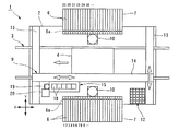
図1および図2に示す部品実装装置1は、基台2の上で図1において左右方向(以下、この方向を単に「X方向」という)に延在するコンベア3を備えている。なお、この実施例においては、図1において下側を部品実装装置1の前側といい、図1において上側を部品実装装置1の後側という。
前記コンベア3は、プリント配線板4をX方向に(例えば図1において右側から左側に)移動させるためのものである。このコンベア3の動作は、部品実装装置1の後述するコントローラ5(図3参照)によって制御される。
(First embodiment)
Hereinafter, an embodiment of a component mounting apparatus and a component mounting method according to the present invention will be described in detail with reference to FIGS.
A
The
基台2における図1において上下方向(以下、この方向を単に「Y方向」という)の両端部には、電子部品P(図2参照)を供給するための多数のテープフィーダ6が装填されている。この実施例においては、このテープフィーダ6によって本発明でいうパーツフィーダが構成されている。
前記多数のテープフィーダ6は、多数の電子部品Pを収納したテープ(図示せず)をY方向に送り、部品吸着部6a(図1参照)に位置決めする構造のもので、基台2の上にフィーダベース7を介して着脱可能に装填されている。これらのテープフィーダ6の動作は、後述するコントローラ5によって制御される。
A large number of
The plurality of
これらのテープフィーダ6は、フィーダベース7上でX方向に並ぶ多数のセット位置にそれぞれ着脱可能に装填されている。多数のセット位置は、X方向に等間隔おいて並ぶ状態でフィーダベース7上に設けられている。各セット位置に装填するテープフィーダ6は、最高の実装効率が得られる最適な配列となるように選択されている。前記最適な配列は、後述するデータ作成装置8(図3参照)が演算によって求める。
These
前記基台2の上には、前記テープフィーダ6上の電子部品Pをプリント配線板4に実装するための部品移動装置9と、この部品移動装置9に吸着・保持された電子部品Pを下方から撮像するための認識カメラ10と、後述する吸着ノズル11(図2参照)を交換するためのノズル交換ステーション12などが設けられている。前記認識カメラ10は、実装可能な電子部品Pであれば全種類の電子部品を撮像できるものが用いられており、Y方向においてコンベア3と多数のテープフィーダ6との間であって、基台2のX方向の略中央部に位置付けられている。
On the
前記多数のテープフィーダ6は、認識カメラ10に最も近接する位置からX方向の一方と他方とに同じ台数並ぶように配置されている。
前記ノズル交換ステーション12は、従来からよく知られたものが用いられており、部品実装装置1の前側であってX方向の一端部に配設されている。
The plurality of
As the
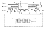
前記部品移動装置9は、前記コンベア3の上方でY方向に延在する2本の固定レール13,13と、これらの固定レール13にY方向へ移動自在に支持された可動レール14と、この可動レール14にX方向へ移動自在に支持されたヘッドユニット15と、前記可動レール14をY方向に移動させるY方向ヘッドユニット移動装置16(図3参照)と、ヘッドユニット15をX方向に移動させるX方向ヘッドユニット移動装置17(図3参照)などによって構成されている。
The
前記ヘッドユニット15には、図2に示すように、電子部品Pを吸着するための複数の吸着ヘッド18と、電子部品Pを下方から撮像するためのスキャンカメラ19と、下方を撮像するための上部カメラ20などが設けられている。前記Y方向ヘッドユニット移動装置16の動作と、X方向ヘッドユニット移動装置17や前記各種カメラ10,19,20の動作は、それぞれ後述するコントローラ5によって制御される。
As shown in FIG. 2, the
前記複数の吸着ヘッド18は、X方向に等間隔おいて並ぶように配設されている。図1に示すヘッドユニット15には、5台の吸着ヘッド18が設けられている。吸着ヘッド18の台数は、部品実装装置の機種によって異なる。
これらの吸着ヘッド18の下端部には、電子部品Pを吸着するための吸着ノズル11がそれぞれ着脱可能に取付けられている。
The plurality of suction heads 18 are arranged so as to be arranged at equal intervals in the X direction. The
The suction nozzles 11 for sucking the electronic components P are detachably attached to the lower ends of these suction heads 18.
この吸着ノズル11は、吸着ヘッド18毎に設けられている昇降装置21(図3参照)によって昇降させられるとともに、吸着ヘッド18毎の回転装置22(図3参照)によって回転させられる。
前記複数の吸着ヘッド18に装着された複数の吸着ノズル11どうしの間隔は、上述したテープフィーダ6のセット位置どうしの間隔と同一の間隔に設定されている。なお、部品実装装置の中には、吸着ノズル11どうしの間隔と前記セット位置どうしの間隔とが一致しないものもある。
The
The intervals between the plurality of
吸着ノズル11は、特定の種類の電子部品Pしか吸着することができないものである。このため、この部品実装装置1においては、1枚のプリント配線板4の全ての部品実装位置に電子部品Pを実装するに当たって必要になる全種類の吸着ノズル11,11…を用意し、その一部を吸着ヘッド18に装着するとともに、他の残りをノズル交換ステーション12に保持させている。吸着ヘッド18に装着する吸着ノズル11(吸着ノズル11を装着する吸着ヘッド18)や、吸着ノズル11を使用して電子部品Pをテープフィーダ6からプリント配線板4上の部品実装位置に実装するときの実装順序などは、後述するデータ作成装置8によって実装効率が高くなるように決められる。
The
前記スキャンカメラ19は、小型の電子部品Pを撮像することができるように構成されており、ヘッドユニット15にスキャンカメラ用駆動装置23(図3参照)を介して支持されている。このスキャンカメラ用駆動装置23は、スキャンカメラ19を吸着ノズル11の下方でX方向に移動させる。
前記上部カメラ20は、プリント配線板4の位置決め用マーク(図示せず)やテープフィーダ6上の電子部品Pなどを上方から撮像するためのもので、ヘッドユニット15に固定されている。
The
The
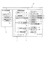
部品実装装置1のコントローラ5は、図3に示すように、演算処理部31と、実装プログラム記憶手段32と、モーター制御部33と、外部入出力部34と、画像処理部35とを備えている。前記演算処理部31は、CPUからなり、後述する各種の演算を行う。この演算処理部31には、ディスプレイ装置からなる表示ユニット36が接続されている。
As shown in FIG. 3, the
前記実装プログラム記憶手段32は、ハードディスク装置や半導体メモリなどによって構成されている。この実装プログラム記憶手段32には、電子部品Pをテープフィーダ6からプリント配線板4上に実装するための全ての動作手順(実装プログラム)が記録されている。
The mounting program storage means 32 is constituted by a hard disk device, a semiconductor memory, or the like. In the mounting program storage means 32, all operation procedures (mounting programs) for mounting the electronic component P on the printed
前記モーター制御部33は、部品実装装置1に使用されている全てのモーターの動作を演算処理部31から送られた制御信号に基づいて制御する。前記外部入出力部34は、部品実装装置1に装備されている各種のセンサ類37や、操作者がデータを入力するためのマウス・キーボード38などが接続されており、センサ類37やマウス・キーボード38からの入力信号を演算処理部31に送る。
The
前記画像処理部35は、前記認識カメラ10、スキャンカメラ19および上部カメラ20などの動作を制御するととともに、これらのカメラで撮像された画像データを演算処理部31に送る。
この実施例によるコントローラ5は、ネットワーク39を介して後述するデータ作成装置8に接続されており、実装に必要なデータをデータ通信によってデータ作成装置8から受け取ることができるように構成されている。
The
The
データ作成装置8は、図3に示すように、演算処理部41と、実装プログラム記憶手段42と、表示ユニット43とを備えている。
演算処理部41は、CPUからなり、実装プログラム記憶手段42に記憶されているプリント配線板に電子部品を実装する際の実装情報{図4(A)参照}と部品情報{図4(B)参照}とに基づいてプリント配線板4上の各部品実装位置毎に最適な実装順序、使用する吸着ノズル11や吸着ヘッド18などを決定するとともに、テープフィーダ6の最適な配列を決める。
As shown in FIG. 3, the
The arithmetic processing unit 41 is composed of a CPU, and mounting information {see FIG. 4 (A)} and component information {FIG. 4 (B) when mounting electronic components on a printed wiring board stored in the mounting program storage means 42. The optimum mounting order for each component mounting position on the printed
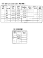
前記実装情報は、プリント配線板4に電子部品Pを実装するに当たって必要になる情報であり、図4(A)に記載済みの値であるプリント配線板4の固有の数値と、同図中には記載されていない(同図では空欄になっている)作成値とがある。
前記プリント配線板4の固有の数値は、プリント配線板4上の各電子部品Pの実装位置を特定するためのランドパターン名と、このランドパターン名に該当する部品実装位置のプリント配線板4上の位置を示す座標Xおよび座標Yと、この部品実装位置に実装される電子部品Pの角度Rと、この部品実装位置に実装される電子部品Pを特定するための部品番号である。
The mounting information is information necessary for mounting the electronic component P on the printed
The specific numerical value of the printed
前記作成値は、各ランドパターンにおける電子部品Pの実装順序と、ランドパターンに電子部品Pを実装するために使用する吸着ノズル11を特定するための使用ノズル番号と、この吸着ノズル11を取付ける吸着ヘッド18を特定するための使用ヘッド番号などである。これらの作成値は、最高の実装効率が得られるようにデータ作成装置8によって最適な値が求められる。
The created value includes the mounting order of the electronic components P in each land pattern, the used nozzle number for specifying the
図4(B)に示す前記部品情報は、前記部品番号に該当する電子部品Pの名称である部品名と、この部品名の電子部品Pを供給するためのテープフィーダ6の位置である。このテープフィーダ6の位置もデータ作成装置8によって最高の実装効率が得られるように最適な位置が求められる。この実施例による部品実装装置1は、これらの実装情報および部品情報の全ての数値が決定された後、これらの情報を用いた実装プログラムに従って実際の実装動作を開始する。
The part information shown in FIG. 4B is a part name which is the name of the electronic part P corresponding to the part number and the position of the
前記各作成値は、データ作成装置8の実装プログラム記憶手段42に記憶させてあるデータ作成プログラムに基づいて演算処理部41が演算を行うことによって求められている。
ここで、前記データ作成プログラムの構成を図5〜図8に示すフローチャートによって説明する。
Each creation value is obtained by the computation processing unit 41 performing computation based on the data creation program stored in the mounting program storage means 42 of the
Here, the configuration of the data creation program will be described with reference to the flowcharts shown in FIGS.
前記演算処理部41は、前記作成値を求めるに当たって、図5に示すフローチャートのステップ101において、データ作成装置8の実装プログラム記憶手段42に記憶されている前記実装情報と部品情報とを読み込む。このときは、前記実装情報と部品情報とのうち、既に判明している図4記載の数値が読み込まれる。
In obtaining the created value, the arithmetic processing unit 41 reads the mounting information and component information stored in the mounting program storage means 42 of the
次に、ステップ102において、吸着ヘッド18に最初に装着する吸着ノズル11を決定する。このときは、生産プログラムの実装情報から電子部品Pの種類毎の個数を求め、これに基づいて使用頻度が高い順に吸着ノズル11を選出する。そして、複数ある吸着ヘッド18のうち例えば図1において左側に位置する吸着ヘッドほど使用頻度の高い吸着ノズル11が装着されるように、各吸着ヘッド18に装着する吸着ノズル11を決定する。なお、吸着ヘッド18に装着する吸着ノズル11を選択するに当たっては、同一種類の吸着ノズル11を複数の吸着ヘッド18に装着する場合もある。
Next, in
その後、ステップ103において、生産プログラム{図4(A)に示す実装情報}を解析し、プリント配線板4上における部品実装位置の分布する範囲の大きさを解析値として算出する。この解析値は、下記に示すように、前記範囲のX方向とY方向の長さを用いる第1の算出方法や、部品実装位置の平均値と標準偏差とを用いる第2の算出方法などによって求めることができる。なお、解析値の算出方法は適宜変更することが可能である。
Thereafter, in
前記第1の算出方法は、図10に示すように実施する。図10は、プリント配線板4上の部品実装位置を模式的に示す平面図である。図10においては、電子部品Pの種類毎に符号を変えるとともに、部品実装位置の形状を変えてある。また、図10は、便宜上、4個の電子部品Aと、3個の電子部品Bと、3個の電子部品Cと、1個ずつの電子部品D,Eとがプリント配線板4に実装されるように描いてある。
The first calculation method is performed as shown in FIG. FIG. 10 is a plan view schematically showing component mounting positions on the printed
第1の算出方法は、全ての部品実装位置のうち、X方向において最もプリント配線板4の外側寄りに位置する2つの部品実装位置の間隔と、Y方向において最もプリント配線板4の外側寄りに位置する2つの部品実装位置の間隔とに基づいて求める方法である。例えば、全ての部品実装位置の座標Xの最大値から最小値を減算した値ΔXと、座標Yの最大値から最小値を減算した値ΔYとを加算することによって解析値を求めることができる。
In the first calculation method, among all the component mounting positions, an interval between two component mounting positions that are located closest to the outside of the printed
この第1の算出方法によれば、前記値ΔXと値ΔYとを単純に加算する他に、値ΔXと値ΔYとをそれぞれ二乗して値ΔX2と値ΔY2とを求め、値ΔX2に値ΔY2を加算した値の平方根を解析値とすることができるし、値ΔXと値ΔYとの積を解析値とすることもできる。 According to the first calculation method, in addition to simply adding the value ΔX and the value ΔY, the value ΔX 2 and the value ΔY 2 are respectively squared to obtain the value ΔX 2 and the value ΔY 2 , and the value ΔX 2 The square root of the value obtained by adding the value ΔY 2 to the analysis value can be used as the analysis value, and the product of the value ΔX and the value ΔY can also be used as the analysis value.
第2の算出方法は、全ての部品実装位置の座標の平均値と標準偏差とを用いる方法である。すなわち、下記の数式(1)に示すように解析値Sを求める。数式(1)において、μXは、全ての部品実装位置の座標Xの平均値を示し、σXは、前記座標Xの標準偏差を示す。また、μYは、全ての部品実装位置の座標Yの平均値を示し、σYは、前記座標Yの標準偏差を示す。KXとKYは、X方向とY方向との配分量を決めるための定数であって、0以上2以下の任意の値である。KXとKYは、例えばヘッドユニット15のX方向の移動速度がY方向の移動速度より速い場合は、KX<KYとして設定してもよい。
解析値S=μX+KXσX+μY+KYσY……(1)
The second calculation method uses an average value and standard deviation of coordinates of all component mounting positions. That is, the analysis value S is obtained as shown in the following formula (1). In Equation (1), μ X represents the average value of the coordinates X of all component mounting positions, and σ X represents the standard deviation of the coordinates X. Μ Y represents an average value of the coordinates Y of all component mounting positions, and σ Y represents a standard deviation of the coordinates Y. K X and K Y are constants for determining the distribution amount in the X direction and the Y direction, and are arbitrary values from 0 to 2. K X and K Y may be set as K X <K Y when the moving speed of the
Analytical value S = μ X + K X σ X + μ Y + K Y σ Y (1)
このように生産プログラムの解析値を算出した後、図5に示すフローチャートのステップ104において、前記解析値が予め定めた設定値未満であるか否かを判定する。この設定値は、部品実装装置1を使用して実験によって求めることができる。
解析値が設定値未満であるときは、プリント配線板4に電子部品Pを実装するときのヘッドユニット15の移動距離が相対的に短くなり、解析値が設定値以上であるときは、実装時のヘッドユニット15の移動距離が相対的に長くなると考えられる。
After calculating the analysis value of the production program in this way, it is determined in
When the analysis value is less than the set value, the moving distance of the
このため、解析値が設定値未満である場合は、ステップ105〜106に示すように、テープフィーダ6の最適な配列を求めた後にこの配列に基づいて電子部品Pの最適な実装順序を求める演算順序(以下、この演算順序を単に「テープフィーダの配列の決定を優先する演算順序」という)で演算を行う。一方、前記解析値が設定値以上である場合は、ステップ107〜108に示すように、電子部品Pの最適な実装順序を求めた後にこの実装順序に基づいてテープフィーダ6の最適な配列を求める演算順序(以下、この演算順序を単に「実装順序の決定を優先する演算順序」という)で演算を行う。
For this reason, when the analysis value is less than the set value, as shown in
この実施例においては、図5のフローチャートによって示すデータ作成プログラムにおけるステップ103〜104を実行するプログラムによって、本発明でいう演算順序設定部が構成されている。すなわち、演算順序設定部は、データ作成装置8の演算処理部41(CPU)で実行されるプログラムで構成されている。
In this embodiment, the calculation order setting unit referred to in the present invention is constituted by a program for executing
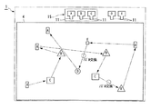
ステップ105においてテープフィーダ6の最適な配列を求めるに当たっては、図6のフローチャートに示すように行う。先ず、図6に示すフローチャートのステップ201において、プリント配線板4上の全実装点(全ての部品実装位置)の座標の平均を算出する。このときは、図11に示すように、全ての部品実装位置A〜Eの座標Xの平均を求めるともに、全ての部品実装位置A〜Eの座標Yの平均を求める。図11においては、平均座標となる位置を符号AV(total)によって示す。
In
図11は、電子部品A〜Eを3本の吸着ヘッド18によってテープフィーダ6からプリント配線板4に移載する場合の一例を示すものである。3本の吸着ヘッド18には、上記ステップ102において決定された3個の吸着ノズル11が装着されている。これら3個の吸着ノズル11は、電子部品A用の吸着ノズル11と、電子部品B用の吸着ノズル11と、電子部品C用の吸着ノズル11である。
FIG. 11 shows an example in which the electronic components A to E are transferred from the
上述したように部品実装位置の座標の平均を求めた後、使用頻度が最も多いテープフィーダ6を前記平均座標AV(total)に最も近接した位置に位置付ける。すなわち、先ず、図6に示すフローチャートのステップ202において、配置位置が未決定であるテープフィーダ6のうち、実装点が最も多いテープフィーダ6(F1)が選択される。そして、ステップ203において、このテープフィーダ6(F1)のセット位置を決める。
After obtaining the average of the coordinates of the component mounting positions as described above, the
このセット位置は、空きセット位置(基台2上の多数のテープフィーダ用セット位置のうち、テープフィーダ6を装着することが決められていないセット位置)のうち、前記平均座標AV(total)に最も近接するセット位置(S1)が選ばれる。図11に示す例においては、電子部品Aが最も多く使用されているから、電子部品Aを供給するためのテープフィーダ6が平均座標AV(total)とX方向において略同一となるような位置に配置される。なお、基台2に設けられている認識カメラ10を用いて電子部品Pを認識する場合は、前記平均座標AV(total)の位置を後述する認識動作開始位置STに変更することが望ましい。
This set position corresponds to the average coordinate AV (total) among the empty set positions (the set positions where the
認識カメラ10によって電子部品Pを認識するためには、ヘッドユニット15を認識カメラ10の上方でX方向(図11においては左右方向)に移動させることによって行う。このX方向への移動は、図11において左から右へ行う場合と、同図において右から左へ行う場合とがある。電子部品Pを認識カメラ10に認識させるためには、電子部品PがX方向へ移動しながら認識カメラ10の上方を横切る必要がある。このため、電子部品Pは、認識カメラ10より前記移動方向の上流側に設定された認識動作開始位置STからX方向へ移動させられる。この認識動作開始位置STは、図11において左から右に移動する場合(同図中に黒丸で示す)と、同図において右から左に移動する場合(同図中に破線の丸で示す)との両方に対応できるように、認識カメラ10の両側方に設定されている。
In order to recognize the electronic component P by the
次に、ステップ204において、配置位置が未決定であるテープフィーダ6のうち、電子部品A用のテープフィーダ6(F1)と同時に電子部品Pを吸着することが可能なテープフィーダ6が存在するか否かを判別する。この判別は、ヘッドユニット15に設けられている吸着ノズル11を参照して行う。図11に示す例においては、電子部品A用吸着ノズル11と隣接する位置に電子部品B用吸着ノズル11が装着されているから、ステップ205において、電子部品A用テープフィーダ6が装填されているセット位置(S1)と隣接するセット位置(同時吸着可能な位置)に電子部品B用テープフィーダ6が配置される。なお、吸着ノズル11どうしの間隔とテープフィーダ6どうしの間隔とが一致しない部品実装装置においては、このステップ204と後述するステップ205は省略する。
Next, in
その後、再びステップ204に戻り、同時に吸着可能なテープフィーダ6がさらに存在するか否かを判定する。図11に示す例においては、電子部品C用のテープフィーダ6が同時吸着可能であるために、このテープフィーダ6が前記電子部品B用テープフィーダ6と隣接するセット位置に配置される。
Thereafter, the process returns to step 204 again, and it is determined whether or not there is an
同時吸着可能なテープフィーダ6が存在しない場合、ステップ206に進み、配置が決まっていないテープフィーダ6の有無を確認する。配置位置が未決定のテープフィーダ6がある場合は、上記ステップ202に戻り、残存している他のテープフィーダ6について上述した手順によってセット位置を決定する。図11に示す例においては、電子部品D用テープフィーダ6と電子部品E用テープフィーダ6とについてセット位置が順次決められる。
If there is no
全てのテープフィーダ6についてセット位置(配列)が決定した後、図5に示すフローチャートのステップ106において、上述したテープフィーダ6の最適な配列に基づいて電子部品Pの最適な実装順序を算出する。このときには、上述した配列で並ぶテープフィーダ6から電子部品Pをプリント配線板4に移載させるときのヘッドユニット15の移動距離が最短になるように実装順序を求める。この最適な実装順序を求めるに当たっては、図7のフローチャートに示すように行う。
After the set positions (arrays) for all the
先ず、図7に示すフローチャートのステップ301において、上述した最適な配列で並ぶテープフィーダ6上の電子部品Pを所定のグループに分ける。この電子部品Pのグループ化は、1回の吸着工程で吸着ノズル11によって吸着される電子部品Pによって一つのグループが構成されるように行う。ここでいう1回の吸着工程とは、ヘッドユニット15がテープフィーダ6の上方に移動した後、電子部品Pが複数の吸着ノズル11に吸着される工程をいう。図11に示す例においては、例えば3個の吸着ノズル11によって同時吸着が可能な電子部品A〜Cを第1のグループG1とすることができる。
First, in
次に、ステップ302において、上述したように分けられた部品の第1のグループG1において、最終吸着点からプリント配線板4への最終実装点までの吸着ヘッド18の移動距離が最短になるように、プリント配線板4への実装順序と、そのときに使用する吸着ヘッド18とを決定する。なお、認識カメラ10を使用して電子部品Pを認識する場合は、最終吸着点の代わりに認識カメラ10の認識終了点を移動距離算出の始点としてもよい。
Next, in
図11に示すプリント配線板4においては、電子部品Aは4箇所に実装され、電子部品Bは3箇所に実装され、電子部品Cは2箇所に実装されるから、1回の吸着工程で3本の吸着ノズル11に電子部品A〜Cを吸着させた場合の実装は、2回行うことができる。すなわち、第1のグループG1の電子部品Pは、図11中に矢印G1Aで示す経路と、矢印G1Bで示す経路とによって実装されるように実装順序と使用吸着ヘッド18とを決めることができる。なお、認識カメラ10を使用して部品の認識を行う場合は、破線の矢印で示すように、認識カメラ10に近接した位置にある部品実装位置を優先させて実装する。
In the printed
第1のグループG1の電子部品Pの実装順序が決められた後、図7に示すフローチャートのステップ303において、実装順序が未決定の実装点(部品実装位置)の有無を判別する。この判別の結果、実装順序を決める実装点が残存している場合は、ステップ301に戻り、全ての電子部品Pの実装順序が決定された場合には、図5に示すフローチャートのステップ109に進む。
After the mounting order of the electronic components P of the first group G1 is determined, in
図11に示す例においては、第1のグループG1の電子部品Pだけでは全ての部品実装位置に電子部品Pを実装することはできないために、第2〜第3のグループG2,G3が設定され、これらのグループ毎に実装順序が決められる。すなわち、前記第1のグループG1による2回の実装が終了した時点で電子部品Cの実装が終了しているから、第1のグループG1に隣接するように、電子部品A,B,Dからなる第2のグループG2が決められる。この第2のグループG2の電子部品Pの実装順序は、図11中に矢印G2で示す最短経路で実装されるように決められる。 In the example shown in FIG. 11, since the electronic component P cannot be mounted at all the component mounting positions only with the electronic component P of the first group G1, the second to third groups G2 and G3 are set. The mounting order is determined for each of these groups. That is, since the mounting of the electronic component C is completed at the time when the second mounting by the first group G1 is completed, the electronic components A, B, and D are adjacent to the first group G1. A second group G2 is determined. The mounting order of the electronic components P of the second group G2 is determined so as to be mounted on the shortest path indicated by an arrow G2 in FIG.
この第2のグループG2による電子部品Pを実装することによって、電子部品Bおよび電子部品Dの実装が終了する。そして、プリント配線板4上に残存している電子部品A用の部品実装位置と電子部品E用の部品実装位置とに電子部品Pを実装するために、第3のグループG3が決められる。第3のグループG3の電子部品Pの実装順序は、図11中に矢印G3で示す最短経路で実装されるように決められる。図11に示す例の場合、第3のグループG3の電子部品Pの実装順序が決められた後、図5に示すステップ109に進む。
The mounting of the electronic component B and the electronic component D is completed by mounting the electronic component P by the second group G2. In order to mount the electronic component P at the component mounting position for the electronic component A and the component mounting position for the electronic component E remaining on the printed
一方、図5のフローチャートのステップ104において、前記解析値が設定値以上であると判定されてステップ107に進んだ場合は、図8のフローチャートに示すように、電子部品Pの実装順序を優先する演算順序で演算が行われる。
すなわち、図8に示すフローチャートのステップ401に示すように、プリント配線板4上の全ての部品実装位置(実装点)に電子部品Pを実装するに当たって、ヘッドユニット15の移動距離の総和が最短になるように、実装順序と使用する吸着ヘッド18とを決定する。
On the other hand, if it is determined in
That is, as shown in
この実施例においては、図8のフローチャートによって示す実装順序算出プログラムと、前記図7のフローチャートによって示す実装順序算出プログラムとによって、本発明でいう実装順序決定部が構成されている。すなわち、実装順序決定部は、データ作成装置8の演算処理部41(CPU)で実行されるプログラムで構成されている。
In this embodiment, the mounting order calculating unit shown in the present invention is constituted by the mounting order calculating program shown by the flowchart of FIG. 8 and the mounting order calculating program shown by the flowchart of FIG. That is, the mounting order determination unit is configured by a program executed by the arithmetic processing unit 41 (CPU) of the
実装順序の決定を優先して実装順序を決める場合の一例を図12〜図15によって説明する。
図12に示す例においては、全ての部品実装位置を最短距離でいわゆる一筆書き状に接続するように実装順序が決められる。
図13に示す例においては、全ての部品実装位置を最短距離でいわゆる一筆書き状に接続するとともに、吸着ノズル11の交換回数が最小になるように実装順序が決められる。
An example of determining the mounting order with priority given to the determination of the mounting order will be described with reference to FIGS.
In the example shown in FIG. 12, the mounting order is determined so that all the component mounting positions are connected in a so-called one-stroke pattern with the shortest distance.
In the example shown in FIG. 13, the mounting order is determined so that all the component mounting positions are connected in a so-called one-stroke pattern with the shortest distance, and the number of replacements of the
図13に示す例においては、同図中に矢印で示すように、電子部品A→C→B→A→B→Cと実装した後に電子部品C用の吸着ノズル11を電子部品E用の吸着ノズル11に交換する。そして、さらに電子部品B→A→Eと実装した後に電子部品Bまたは電子部品E用の吸着ノズル11を電子部品D用の吸着ノズル11に交換し、電子部品Dと電子部品Aとを実装する。
In the example shown in FIG. 13, as indicated by an arrow in the figure, after the electronic component A → C → B → A → B → C is mounted, the
上述した図12と図13とに示す例においては、電子部品Pを吸着するためにヘッドユニット15がプリント配線板4上からテープフィーダ6上へ移動するときの距離、すなわち吸着工程におけるヘッドユニット15の移動距離は加算していない。また、全ての電子部品Pをスキャンカメラ19によって認識させ、ヘッドユニット15が認識カメラ10の上を通過することにより増える移動距離も加算してはいない。吸着工程におけるヘッドユニット15の移動距離を加算する場合や、認識カメラ10によって認識させるためのヘッドユニット15の移動距離を加算する場合には、図14および図15に示すように実装順序を決めることができる。
In the example shown in FIG. 12 and FIG. 13 described above, the distance when the
吸着工程の移動距離を含めてヘッドユニット15の移動距離を求めるためには、テープフィーダ6の平均的な吸着位置を求め、この吸着位置で電子部品Pを吸着してからプリント配線板4に実装すると仮定して前記移動距離を計算する。図14および図15に示す例においては、前記テープフィーダ6の平均的な吸着位置を符号AV(P)によって示す。
In order to obtain the moving distance of the
図14に示す例は、後述する第1および第2の条件を満たしながらヘッドユニット15の移動距離が可及的短くなるように電子部品Pの実装順序を決めるときの一例である。
前記第1の条件とは、吸着ノズル11の交換回数を可及的少なくすることである。
前記第2の条件とは、全ての電子部品Pを認識カメラ10によって認識することである。
The example shown in FIG. 14 is an example when the mounting order of the electronic components P is determined so that the moving distance of the
The first condition is to reduce the number of replacements of the
The second condition is that the
図14に示す例においては、同図中に矢印(1)で示すように、電子部品A→C→Bという順序で実装して吸着位置に戻り、次に、矢印(2)に示すように、電子部品B→A→Cという順序で実装してから吸着位置に戻る。その後、矢印(3)に示すように、電子部品D→B→Aという順序で実装してから吸着位置に戻り、矢印(4)に示すように、電子部品E→Aという順序で実装する。 In the example shown in FIG. 14, as shown by the arrow (1) in the figure, the electronic components are mounted in the order of A → C → B and returned to the suction position, and then as shown by the arrow (2). Then, after mounting in the order of electronic components B → A → C, it returns to the suction position. After that, the electronic components are mounted in the order of D → B → A as shown by the arrow (3) and then returned to the suction position, and the electronic components are mounted in the order of E → A as shown by the arrow (4).
図15に示す例は、上記図14に示した例にさらにノズル交換ステーション12で吸着ノズル11を交換してからヘッドユニット15を吸着位置に戻すという第3の条件を付加した場合の一例である。図15に示す例においては、同図中に矢印(2)で示すように電子部品B→A→Cという順序で実装した後、ノズル交換ステーション12を経由してから吸着位置に戻す。
The example shown in FIG. 15 is an example in the case where the third condition that the
ノズル交換ステーション12においては、電子部品C用の吸着ノズル11を電子部品D用の吸着ノズル11に交換する。その後、矢印(3)に示すように電子部品D→B→Aという順序で実装した後、ノズル交換ステーション12で電子部品B用または電子部品D用の吸着ノズル11を電子部品E用の吸着ノズル11に交換してから吸着位置に戻る。そして、矢印(4)に示すように、電子部品E→Aという順序で実装を行う。
In the
図8のフローチャートに示すプログラムによって最適な実装順序を求めた後、図9のフローチャートに示すプログラムによって、前記実装順序に基づいてテープフィーダ6の配列を求める。
すなわち、先ず、図9に示すフローチャートのステップ501において、多数のテープフィーダ6の中から任意の1台のテープフィーダ6(F)を選択する。次に、この選択されたテープフィーダ6(F)の電子部品Pが実装されるプリント配線板4上の全ての部品実装位置の平均座標{AV(F)}を算出する(ステップ502)。そして、残存している空きセット位置のうち、前記平均座標{AV(F)}に最も近接する位置にあるセット位置に前記選択されたテープフィーダ6(F)を配置する(ステップ503)。
After obtaining the optimum mounting order by the program shown in the flowchart of FIG. 8, the arrangement of the
That is, first, in
これらのステップ501〜503に示す設定動作を全てのテープフィーダ6について行う(ステップ504)ことによって、全ての電子部品Pを部品実装位置に近接した位置にそれぞれ供給することができるようになる。すなわち、最適な実装順序を実現可能な位置にテープフィーダ6を配置することができ、最適な実装順序に基づいてテープフィーダ6の最適な配列を求めることができる。
By performing the setting operation shown in
この実施例においては、図9のフローチャートによって示す配列算出プログラムと、前記図6のフローチャートによって示す配列算出プログラムとによって、本発明でいう配列決定部が構成されている。すなわち、配列決定部は、データ作成装置8の演算処理部41(CPU)で実行されるプログラムで構成されている。
In this embodiment, the sequence determination unit referred to in the present invention is constituted by the sequence calculation program shown by the flowchart of FIG. 9 and the sequence calculation program shown by the flowchart of FIG. That is, the arrangement determining unit is configured by a program executed by the arithmetic processing unit 41 (CPU) of the
ここで、図9に示す手順によってテープフィーダ6の配列を求める場合の一例を図16によって説明する。
図16に示すプリント配線板4を使用する場合は、電子部品A〜E用のテープフィーダ6が使用される。図9のステップ501でたとえば電子部品Bを供給するためのテープフィーダ6が選択された場合、ステップ502において、プリント配線板4上にある3箇所の電子部品B用の部品実装位置の平均座標AV(B)が求められる。
Here, an example of obtaining the arrangement of the
When the printed
そして、ステップ503において、平均座標AV(B)に最も近接する位置に電子部品B用のテープフィーダ6が配置される。なお、ステップ501においては、配置位置が未決定のテープフィーダ6のうち、使用頻度が最も高いテープフィーダ6を選択するしてもよい。図16においては、電子部品A用の部品実装位置の平均座標を符号AV(A)で示し、電子部品C用の部品実装位置の平均座標を符号AV(C)で示す。
図16は、電子部品A用のテープフィーダ6が2番目に選択され、以下順に電子部品E、電子部品D、電子部品Cの順で選択された場合を示している。
In
FIG. 16 shows a case where the
このように全てのテープフィーダ6について最適な配列を求めた後、図5に示すフローチャートのステップ109に進む。
図5のステップ109においては、上述したステップ105〜108で求められた実装情報(部品実装位置毎の実装順序、使用ノズル番号、使用ヘッド番号)と部品情報(フィーダ位置)とがデータ作成装置8の実装プログラム記憶手段42に書き加えられる。その後、この実装プラグラム記憶手段42に記憶されている実装情報の全てのデータと、部品情報の全てのデータとが部品実装装置1の実装プログラム記憶手段32に読み込まれ、部品実装装置1において実際の実装動作が開始される。
After obtaining the optimal arrangement for all the
In
上述したように構成された部品実装装置1においては、テープフィーダ6の最適な配列を求めた後にこの配列に基づいて電子部品Pの最適な実装順序を求める演算順序(テープフィーダ6の配列の決定を優先する演算順序)と、電子部品Pの最適な実装順序を求めた後にこの実装順序に基づいてテープフィーダ6の最適な配列を求める演算順序(実装順序の決定を優先する演算順序)とのうち、プリント配線板4上における部品実装位置の分布する範囲の大きさに対応した演算順序を選択することができる。
In the
このため、前記テープフィーダ6の配列の決定を優先する演算順序で演算した場合の実装効率と、前記実装順序の決定を優先する演算順序で演算した場合の実装効率とを比較して最適な演算順序を決める装置に較べて、少ない演算量で同等の結果を得ることが可能になる。
したがって、この実施例によれば、演算時間がそれほど長くなることなく、高い実装効率が得られるようにテープフィーダ6の最適な配列と電子部品Pの最適な実装順序とを決めることが可能な部品実装装置を提供することができる。
For this reason, the optimal calculation is performed by comparing the mounting efficiency when the calculation order giving priority to the determination of the arrangement of the
Therefore, according to this embodiment, the components that can determine the optimal arrangement of the
また、この実施例による部品実装方法によれば、テープフィーダ6の配列の決定を優先する演算順序と、電子部品Pの実装順序の決定を優先する演算順序とのうち、実装対象となるプリント配線板4に適合した一方の演算順序を選択することができる。このため、前記2通りの演算順序でそれぞれ演算を行ってその結果から実装効率が高くなる演算順序を導き出す方法を採る場合に較べて、少ない演算量で同等の結果を得ることができる。
したがって、この実施例によれば、演算時間がそれほど長くなることなく、高い実装効率が得られるようにパーツフィーダの最適な配列と電子部品Pの最適な実装順序とを決めることが可能な部品実装方法を提供することができる。
In addition, according to the component mounting method according to this embodiment, the printed wiring to be mounted among the calculation order that prioritizes the determination of the arrangement of the
Therefore, according to this embodiment, the component mounting that can determine the optimal arrangement of the parts feeder and the optimal mounting order of the electronic components P so that high mounting efficiency can be obtained without requiring much calculation time. A method can be provided.
(第2の実施例)
テープフィーダ6の配列や電子部品Pの実装順序を演算によって求めるときの所要時間は、1枚のプリント配線板4に形成されている部品実装位置の総数(実装点数)に対応して増減する。このため、実装点数が相対的に少なく、前記演算の結果を得るために必要な時間が相対的に短くなると予測できる場合は、図17のフローチャートに示すように、テープフィーダ6の配列の決定を優先する演算順序で演算を行った結果と、電子部品Pの実装順序を優先する演算順序で演算を行った結果とを比較し、実装効率が高くなる演算結果を採用することができる。
(Second embodiment)
The time required for calculating the arrangement of the
図17に示すフローチャートは、前記図5に示すフロチャートのステップ102とステップ103との間に判断ステップ111を挿入するとともに、このステップ111から分岐した一連の処理ステップ112〜118を追加したものである。図17において、図5によって説明したステップについては、同一符号を付し詳細な説明を適宜省略する。
In the flowchart shown in FIG. 17, a
図17に示すフローチャートのステップ111においては、実装点数(部品実装位置の総数)が予め定めた設定数以上であるか否かを判定する。この設定数としては、たとえば100とすることができる。1枚のプリント配線板4上に実装点数が前記設定数以上である場合は、上述した実施例1で説明した方法を実施し、実装点数が前記設定数以上ではないとき(設定数未満であるとき)には、ステップ112に進む。
In
すなわち、この第2の実施例による部品実装装置1は、本発明でいう演算順序設定部による演算順序の設定(ステップ103,104)を、プリント配線板4に実装される電子部品Pの総数が予め定めた設定数以上であるときに行う構成が採られている。また、この実施例による演算順序設定部は、図17に示すステップ103,104と、ステップ111〜118とからなるプログラムによって構成されている。この第2の実施例による演算順序設定部によって、本願発明の請求項3に記載した演算順序設定部が構成されている。
That is, in the
前記ステップ112においては、テープフィーダ6の最適な配列を算出する。すなわち、ステップ112においては、図5に示すフローチャートのステップ105で実施する処理と同一の処理を行う。
次に、ステップ113において、前記ステップ112で算出したテープフィーダ6の配列に基づいて電子部品Pの最適な実装順序を算出する。すなわち、ステップ113においては、図5に示すフローチャートのステップ106で実施する処理と同一の処理を行う。
In
Next, in
また、このステップ113においては、ステップ112で求めた配列のテープフィーダ6からステップ113で求めた実装順序で電子部品Pを実装するときのヘッドユニット15の移動距離を算出する。
このヘッドユニット15の移動距離は、ステップ114において、データ作成装置8の実装プログラム記憶手段42に保存する。
In
The moving distance of the
しかる後、ステップ115において、電子部品Pの最適な実装順序を算出する。このステップ115においては、図5に示すフローチャートのステップ107で実施する処理と同一の処理を行う。次いで、前記ステップ115において算出された最適な実装順序に基づいてテープフィーダ6の最適な配列を求める(ステップ116)。このステップ116においては、図5に示すフローチャートのステップ108で実施する処理と同一の処理を行う。
Thereafter, in
また、ステップ116においては、このステップ116で求めた配列のテープフィーダ6からステップ115で求めた実装順序で電子部品Pを実装するときのヘッドユニット15の移動距離を算出する。この移動距離は、ステップ117において、データ作成装置8の実装プログラム記憶手段42に保存する。
In
次に、ステップ118において、前記ステップ114で保存したヘッドユニット15の移動距離と、前記ステップ117で保存したヘッドユニット15の移動距離とを比較する。この比較の結果、移動距離が短くなる方、言い換えれば実装効率が高くなる方のテープフィーダ6の配列および電子部品Pの実装順序を選択し、ステップ109に進む。
Next, in
ステップ109においては、ステップ105〜108で求められたテープフィーダ6の配列と電子部品Pの実装順序との他に、ステップ118で選択したテープフィーダ6の配列と電子部品Pの実装順序とを前記データ作成装置8の実装プログラム記憶手段42に保存する。
In
この第2の実施例においては、本発明でいう演算順序設定部による演算順序の設定を、プリント配線板4に実装される電子部品Pの総数が予め定めた設定数以上であるときに行うように構成されている。このため、この第2の実施例によれば、1枚のプリント配線板4に電子部品Pを大量に実装する場合であっても、パーツフィーダの配列と電子部品Pの実装順序とを、短時間にかつ実装効率がより一層高くなるように求めることができる。
この結果、この実施例によれば、大量の電子部品Pを速く実装することが可能な、生産状況に適合した部品実装装置を提供することができる。
In the second embodiment, the calculation order setting by the calculation order setting unit referred to in the present invention is performed when the total number of electronic components P mounted on the printed
As a result, according to this embodiment, it is possible to provide a component mounting apparatus that can quickly mount a large number of electronic components P and that is suitable for production conditions.
この第2の実施例に示す演算順序設定部は、上記ステップ112〜118に示すように、前記プリント配線板4に実装される電子部品Pの総数が予め定めた設定数未満である場合、前記配列決定部がパーツフィーダの配列を求めた後にこの配列に基づいて前記実装順序決定部が電子部品Pの実装順序を求める演算と、前記実装順序決定部が電子部品Pの実装順序を求めた後にこの実装順序に基づいて前記配列決定部がパーツフィーダの配列を求める演算とを行い、これらの演算の結果を比較して実装効率が高くなる一方のパーツフィーダの配列と電子部品の実装順序とを採用する構成が採られている。
When the total number of electronic components P mounted on the printed
このため、この実施例によれば、プリント配線板4に実装する電子部品Pの個数が少ない場合、より一層確実に実装効率の向上を図ることが可能な部品実装装置を提供することができる。
For this reason, according to this embodiment, when the number of electronic components P to be mounted on the printed
プリント配線板4上における部品実装位置の分布する範囲の大きさは、上述した第1の実施例と第2の実施例とに示したように、前記部品実装位置のプリント配線板4上における座標の最大値と最小値との差ΔX,ΔYに基づいて求めることができる。
この構成を採ることにより、プリント配線板4上における部品実装位置の分布する範囲の大きさを簡単な演算によって求めることができるから、例えば画像処理によって求める場合に較べて所要時間が短くてよいし、上部カメラ20を使用する必要もない。したがって、テープフィーダ6の最適な配列と電子部品Pの最適な実装順序とを短時間にかつ容易に求めることが可能になる。
The size of the distribution range of the component mounting positions on the printed
By adopting this configuration, the size of the distribution range of the component mounting positions on the printed
上述した第1の実施例と第2の実施例とにおいては、プリント配線板4上における部品実装位置の分布する範囲の大きさを、部品実装位置のプリント配線板4上における座標の平均値μX,μYと標準偏差σX,σYとに基づいて求めることができる。
In the first embodiment and the second embodiment described above, the size of the distribution range of the component mounting positions on the printed
この構成を採ることにより、プリント配線板4上における部品実装位置の分布する範囲の大きさを演算のみによって求めることができるから、例えば画像処理によって求める場合に較べて所要時間が短くてよいし、上部カメラ20を使用する必要もない。また、部品実装位置のばらつきの程度に対応した値を求めることができるから、前記範囲の大きさをより一層正確に求めることができる。
したがって、使用するプリント配線板4に対応させて、テープフィーダ6の最適な配列と電子部品Pの最適な実装順序とを短時間にかつ容易に求めることが可能になる。
By adopting this configuration, it is possible to determine the size of the distribution range of the component mounting positions on the printed
Accordingly, it is possible to easily find the optimum arrangement of the
上述した第1、第2の実施例においては、本発明でいうパーツフィーダとしてテープフィーダ6を用いる例を示したが、本発明は、このような限定にとらわれることはなく、たとえば電子部品Pをスティック状に一列に並べて供給するスティックフィーダや、バルク部品を供給するためのバルクフィーダなどをパーツフィーダとして用いることができる。
In the first and second embodiments described above, the example in which the
上述した第1、第2の実施例においては、認識カメラ10とスキャンカメラ19とを装備した部品実装装置1を用いる例を示したが、本発明は、前記両カメラのうちいずれか一方しか備えていない部品実装装置にも適用することができる。
In the first and second embodiments described above, the example using the
上述した第1、第2の実施例においては、データ作成装置8を部品実装装置1のコントローラ5とは別体に形成する例を示したが、データ作成装置8は、前記コントローラ5に内蔵させることができる。この構成を採る場合は、コントローラ5の実装プログラム記憶手段32にデータ作成プログラムを記憶させ、コントローラ5の演算処理部31によってデータ作成プログラムを実行する。
In the first and second embodiments described above, an example in which the
第2の実施例においては、プリント配線板4に実装する電子部品Pの個数が設定数未満の場合にテープフィーダ6の配列の決定を優先する演算順序で演算した結果と、電子部品Pの実装順序の決定を優先する演算順序で演算した結果とを比較する例を示したが、電子部品Pの個数が設定数未満の場合は、前記2通りの演算順序のうち予め決めた一方の演算順序でのみ演算を行うようにしてもよい。
In the second embodiment, when the number of electronic components P to be mounted on the printed
第1、第2の実施例においては、ヘッドユニット15の移動距離が可及的短くなるように最適な解(テープフィーダ6の配列と電子部品Pの実装順序)を求める例を示したが、ヘッドユニット15の移動時間が可及的短くなるように最適な解を求める構成とすることもできる。
In the first and second embodiments, an example in which an optimal solution (the arrangement of the
1…部品実装装置、2…基台、4…プリント配線板、5…コントローラ、6…テープフィーダ、8…データ作成装置、9…部品移動装置、10…認識カメラ、11…吸着ノズル、12…ノズル交換ステーション、15…ヘッドユニット、18…吸着ヘッド、19…スキャンカメラ、31,41…演算処理部、32,42…実装プログラム記憶手段。
DESCRIPTION OF
Claims (6)
これらのパーツフィーダ上の電子部品を吸着ノズルに吸着させてプリント配線板の部品実装位置に実装する部品移動装置と、
前記パーツフィーダの最適な配列を演算によって求める配列決定部と、
前記電子部品の最適な実装順序を演算によって求める実装順序決定部とを備え、
前記配列決定部によって求められた配列とされたパーツフィーダの電子部品を、前記実装順序決定部によって求められた実装順序でプリント配線板に実装する部品実装装置において、
前記プリント配線板上における前記部品実装位置の分布する範囲の大きさが予め定めた値未満である場合は、前記配列決定部が求めたパーツフィーダの配列に基づいて前記実装順序決定部が電子部品の実装順序を求め、前記範囲の大きさが前記値以上である場合は、前記実装順序決定部が求めた電子部品の実装順序に基づいて前記配列決定部がパーツフィーダの配列を求めるように前記配列決定部と実装順序決定部との演算順序を設定する演算順序設定部を備えている部品実装装置。 Many parts feeders that supply electronic components,
A component moving device that adsorbs electronic components on these parts feeders to a suction nozzle and mounts them on a component mounting position on a printed wiring board; and
An arrangement determining unit for obtaining an optimum arrangement of the parts feeder by calculation;
A mounting order determination unit that obtains the optimal mounting order of the electronic components by calculation;
In the component mounting apparatus for mounting the electronic parts of the parts feeder determined as the array determined by the array determining unit on the printed wiring board in the mounting order determined by the mounting order determining unit,
When the size of the distribution range of the component mounting positions on the printed wiring board is less than a predetermined value, the mounting order determining unit determines whether the mounting order determining unit is an electronic component based on the arrangement of the parts feeder obtained by the array determining unit. If the size of the range is equal to or greater than the value, the arrangement determining unit determines the arrangement of the parts feeder based on the mounting order of the electronic components obtained by the mounting order determining unit. A component mounting apparatus including a calculation order setting unit that sets a calculation order of an arrangement determination unit and a mounting order determination unit.
これらの演算の結果を比較して実装効率が高くなる一方の演算順序を採用する部品実装装置。 The component mounting apparatus according to claim 1, wherein when the total number of electronic components mounted on the printed wiring board is less than a predetermined number, the arrangement determining unit obtains an arrangement of parts feeders. After that, the mounting order determination unit calculates the electronic component mounting order based on this arrangement, and after the mounting order determination unit determines the electronic component mounting order, the arrangement determination unit determines the parts based on the mounting order. Perform the operation to obtain the feeder array,
A component mounting apparatus that employs one of the calculation orders that increases the mounting efficiency by comparing the results of these calculations.
前記パーツフィーダ上の電子部品を吸着ノズルに吸着させてプリント配線板の部品実装位置に実装するときの最適な実装順序を求める工程と、
最適な配列のパーツフィーダの電子部品を最適な実装順序でプリント配線板に実装する工程とを有する部品実装方法において、
前記プリント配線板上における前記部品実装位置の分布する範囲の大きさが予め定めた値未満である場合は、パーツフィーダの最適な配列を求めた後にこの配列に基づいて電子部品の最適な実装順序を求め、
前記範囲の大きさが前記値以上である場合は、電子部品の最適な実装順序を求めた後にこの実装順序に基づいてパーツフィーダの最適な配列を求める部品実装方法。 A process for obtaining an optimal arrangement of a large number of parts feeders for supplying electronic components;
A step of obtaining an optimal mounting order when the electronic component on the parts feeder is sucked by a suction nozzle and mounted at a component mounting position of a printed wiring board;
In a component mounting method including a step of mounting electronic components of an optimally arranged parts feeder on a printed wiring board in an optimal mounting order,
When the size of the distribution range of the component mounting positions on the printed wiring board is less than a predetermined value, the optimal mounting order of electronic components based on this array is obtained after obtaining the optimal array of parts feeders Seeking
A component mounting method for obtaining an optimal arrangement of parts feeders based on the mounting order after determining an optimal mounting order of electronic components when the size of the range is equal to or greater than the value.
Priority Applications (1)
| Application Number | Priority Date | Filing Date | Title |
|---|---|---|---|
| JP2008308283A JP5145200B2 (en) | 2008-12-03 | 2008-12-03 | Component mounting apparatus and component mounting method |
Applications Claiming Priority (1)
| Application Number | Priority Date | Filing Date | Title |
|---|---|---|---|
| JP2008308283A JP5145200B2 (en) | 2008-12-03 | 2008-12-03 | Component mounting apparatus and component mounting method |
Publications (2)
| Publication Number | Publication Date |
|---|---|
| JP2010135463A JP2010135463A (en) | 2010-06-17 |
| JP5145200B2 true JP5145200B2 (en) | 2013-02-13 |
Family
ID=42346477
Family Applications (1)
| Application Number | Title | Priority Date | Filing Date |
|---|---|---|---|
| JP2008308283A Active JP5145200B2 (en) | 2008-12-03 | 2008-12-03 | Component mounting apparatus and component mounting method |
Country Status (1)
| Country | Link |
|---|---|
| JP (1) | JP5145200B2 (en) |
Families Citing this family (5)
| Publication number | Priority date | Publication date | Assignee | Title |
|---|---|---|---|---|
| JP5535032B2 (en) * | 2010-10-27 | 2014-07-02 | 株式会社日立ハイテクインスツルメンツ | Component mounting system, component mounting setting device, component mounting setting program, and component mounting method |
| JP5861037B2 (en) * | 2012-06-08 | 2016-02-16 | パナソニックIpマネジメント株式会社 | Component mounting apparatus and component mounting method |
| JP6139948B2 (en) * | 2013-04-05 | 2017-05-31 | ヤマハ発動機株式会社 | Component mounting equipment |
| WO2015059754A1 (en) * | 2013-10-21 | 2015-04-30 | 富士機械製造株式会社 | Mounting device and management device |
| US11304351B2 (en) * | 2018-03-13 | 2022-04-12 | Fuji Corporation | Mounting device, information processing device, and mounting method |
Family Cites Families (5)
| Publication number | Priority date | Publication date | Assignee | Title |
|---|---|---|---|---|
| JP3476485B2 (en) * | 1992-09-11 | 2003-12-10 | 松下電器産業株式会社 | Component mounting order determination method |
| JPH08167796A (en) * | 1994-12-15 | 1996-06-25 | Matsushita Electric Ind Co Ltd | Electronic parts mounting method |
| JPH0951198A (en) * | 1995-08-07 | 1997-02-18 | Matsushita Electric Ind Co Ltd | Mounting data-preparing method |
| JP3504394B2 (en) * | 1995-09-08 | 2004-03-08 | 松下電器産業株式会社 | How to create component array data |
| JP2000312094A (en) * | 1999-04-28 | 2000-11-07 | Matsushita Electric Ind Co Ltd | Optimum method for mounting electronic part |
-
2008
- 2008-12-03 JP JP2008308283A patent/JP5145200B2/en active Active
Also Published As
| Publication number | Publication date |
|---|---|
| JP2010135463A (en) | 2010-06-17 |
Similar Documents
| Publication | Publication Date | Title |
|---|---|---|
| JP5683006B2 (en) | Component mounting apparatus, information processing apparatus, information processing method, and board manufacturing method | |
| JP5145200B2 (en) | Component mounting apparatus and component mounting method | |
| JP6522735B2 (en) | Component mounting machine | |
| CN106391397A (en) | Glue spraying device and determination method of border track | |
| KR20000011720A (en) | mounting method of electronic parts | |
| US11363751B2 (en) | Mounting order determination device, mounting order examination device, mounting order determination method, and mounting order examination method | |
| JP5775807B2 (en) | Information providing apparatus, information providing method, and component mounting system | |
| JP5331859B2 (en) | Mounting board manufacturing system and mounting board manufacturing method | |
| JP4995745B2 (en) | Component mounting equipment | |
| JP2008141183A (en) | Method for mounting component | |
| JP2012134303A (en) | Electronic component attachment device, and electronic component attachment method | |
| JPH09312494A (en) | Supply of component to mounting machine | |
| JP5064758B2 (en) | Data creation device and surface mounter | |
| JP2008277772A (en) | Method of manufacturing substrate | |
| JP4804402B2 (en) | Component mounting order determination method | |
| JP2008277770A (en) | Component mounting method | |
| JP6043993B2 (en) | Component mounting apparatus, information processing apparatus, information processing method, and board manufacturing method | |
| JP4954698B2 (en) | Surface mounter and control method of surface mounter | |
| JP5663151B2 (en) | Component mounting method and component mounting apparatus | |
| JP2007109893A (en) | Method for determining order of part mounting | |
| JP4521982B2 (en) | Electronic device mounting apparatus and feeder bank | |
| JP7186519B2 (en) | Temporary storage area positioning method and temporary storage area positioning device in backup device | |
| JP2008218538A (en) | System and method for mounting electronic component | |
| JP5622886B2 (en) | Component mounting method | |
| JP6515343B2 (en) | Component mounting method and component mounting apparatus |
Legal Events
| Date | Code | Title | Description |
|---|---|---|---|
| A621 | Written request for application examination |
Free format text: JAPANESE INTERMEDIATE CODE: A621 Effective date: 20110628 |
|
| TRDD | Decision of grant or rejection written | ||
| A977 | Report on retrieval |
Free format text: JAPANESE INTERMEDIATE CODE: A971007 Effective date: 20121025 |
|
| A01 | Written decision to grant a patent or to grant a registration (utility model) |
Free format text: JAPANESE INTERMEDIATE CODE: A01 Effective date: 20121106 |
|
| A01 | Written decision to grant a patent or to grant a registration (utility model) |
Free format text: JAPANESE INTERMEDIATE CODE: A01 |
|
| A61 | First payment of annual fees (during grant procedure) |
Free format text: JAPANESE INTERMEDIATE CODE: A61 Effective date: 20121126 |
|
| FPAY | Renewal fee payment (event date is renewal date of database) |
Free format text: PAYMENT UNTIL: 20151130 Year of fee payment: 3 |
|
| R150 | Certificate of patent or registration of utility model |
Ref document number: 5145200 Country of ref document: JP Free format text: JAPANESE INTERMEDIATE CODE: R150 Free format text: JAPANESE INTERMEDIATE CODE: R150 |
|
| R250 | Receipt of annual fees |
Free format text: JAPANESE INTERMEDIATE CODE: R250 |
|
| R250 | Receipt of annual fees |
Free format text: JAPANESE INTERMEDIATE CODE: R250 |
|
| R250 | Receipt of annual fees |
Free format text: JAPANESE INTERMEDIATE CODE: R250 |
|
| R250 | Receipt of annual fees |
Free format text: JAPANESE INTERMEDIATE CODE: R250 |
|
| R250 | Receipt of annual fees |
Free format text: JAPANESE INTERMEDIATE CODE: R250 |
|
| R250 | Receipt of annual fees |
Free format text: JAPANESE INTERMEDIATE CODE: R250 |
|
| R250 | Receipt of annual fees |
Free format text: JAPANESE INTERMEDIATE CODE: R250 |
|
| R250 | Receipt of annual fees |
Free format text: JAPANESE INTERMEDIATE CODE: R250 |
|
| R250 | Receipt of annual fees |
Free format text: JAPANESE INTERMEDIATE CODE: R250 |