JP5083000B2 - 電子部品装置及び電子部品装置の製造方法 - Google Patents
電子部品装置及び電子部品装置の製造方法 Download PDFInfo
- Publication number
- JP5083000B2 JP5083000B2 JP2008099753A JP2008099753A JP5083000B2 JP 5083000 B2 JP5083000 B2 JP 5083000B2 JP 2008099753 A JP2008099753 A JP 2008099753A JP 2008099753 A JP2008099753 A JP 2008099753A JP 5083000 B2 JP5083000 B2 JP 5083000B2
- Authority
- JP
- Japan
- Prior art keywords
- electrode
- electronic component
- metal part
- metal
- tin
- Prior art date
- Legal status (The legal status is an assumption and is not a legal conclusion. Google has not performed a legal analysis and makes no representation as to the accuracy of the status listed.)
- Expired - Fee Related
Links
Images


Classifications
-
- H—ELECTRICITY
- H10—SEMICONDUCTOR DEVICES; ELECTRIC SOLID-STATE DEVICES NOT OTHERWISE PROVIDED FOR
- H10W—GENERIC PACKAGES, INTERCONNECTIONS, CONNECTORS OR OTHER CONSTRUCTIONAL DETAILS OF DEVICES COVERED BY CLASS H10
- H10W72/00—Interconnections or connectors in packages
- H10W72/071—Connecting or disconnecting
- H10W72/072—Connecting or disconnecting of bump connectors
-
- H—ELECTRICITY
- H10—SEMICONDUCTOR DEVICES; ELECTRIC SOLID-STATE DEVICES NOT OTHERWISE PROVIDED FOR
- H10W—GENERIC PACKAGES, INTERCONNECTIONS, CONNECTORS OR OTHER CONSTRUCTIONAL DETAILS OF DEVICES COVERED BY CLASS H10
- H10W90/00—Package configurations
- H10W90/701—Package configurations characterised by the relative positions of pads or connectors relative to package parts
- H10W90/721—Package configurations characterised by the relative positions of pads or connectors relative to package parts of bump connectors
- H10W90/724—Package configurations characterised by the relative positions of pads or connectors relative to package parts of bump connectors between a chip and a stacked insulating package substrate, interposer or RDL
Landscapes
- Wire Bonding (AREA)
Description
また、基板上に多数の島状半田ペースト領域を形成し、各島状半田ペースト領域に金属ボールを配置し、その後基板上の半田を溶融させる半田ボールの製造方法が提案されている。(特許文献2参照)
更に、錫(Sn)を主成分とする2種類以上の合金粉末をフラックスと混合して、全体として所望の重量比になるように構成し、銅(Cu)ランドと電子部品間で半田の組成を傾斜分布させ、銅(Cu)ランドに対しては濡れ性を向上させ、電子部品に対しては半田付け強度を向上させたことを特徴とするクリーム半田も提案されている。(特許文献3参照)
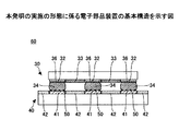
まず、図2を参照して、本発明の実施の形態に係る電子部品装置の基本構造を説明し、次に、図3乃至図5を参照して、該構造の具体的構造を説明する。
図2に示すように、本発明の実施の形態に係る電子部品装置60にあっては、支持基板(パッケージ基板)30が、外部接続部たる半田バンプ34を介して回路配線基板(マザーボード)40に電気的に接続されている。
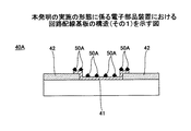
次に、上述の基本構造を備えた電子部品装置における回路配線基板40の具体的構造(第1の例乃至第3の例)について、図3乃至図5を参照して説明する。なお、図3乃至図5において、図2に示した箇所と同じ箇所には同じ符号を付して、その詳細な説明を省略する。
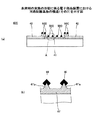
次に、上述の第1乃至第3の例に係る配線回路基板40A乃至40Cを備えた電子部品装置の製造方法について説明する。
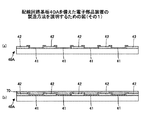
図8乃至図11を参照して、配線回路基板40Aを備えた電子部品装置の製造方法について説明する。
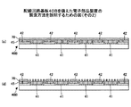
図12乃至図16を参照して、配線回路基板40Bを備えた電子部品装置の製造方法について説明する。なお、図12乃至図16において、図8乃至図11を参照して説明した箇所と同じ箇所については、同じ符号を付してその説明を省略する。
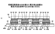
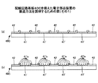
図17乃至図19を参照して、配線回路基板40Cを備えた電子部品装置の製造方法について説明する。なお、図17乃至図19において、図8乃至図16を参照して説明した箇所と同じ箇所については、同じ符号を付してその説明を省略する。
(付記1)
銅(Cu)を含む電極を主面に備えた回路配線基板と、
錫(Sn)を含み、前記電極に接続される外部接続部を主面に備えた電子部品と、を有し、
前記電極と前記外部接続部との界面の一部に、錫(Sn)と親和性を有する金属部が形成されていることを特徴とする電子部品装置。
(付記2)
付記1記載の電子部品装置であって、
前記金属部は、前記回路配線基板の前記電極上に島状に形成されていることを特徴とする電子部品装置。
(付記3)
付記1又は2いずれか一項記載の電子部品装置であって、
前記金属部は、コバルト(Co)、鉄(Fe)、ニッケル(Ni)、又はマンガン(Mn)を含むことを特徴とする電子部品装置。
(付記4)
付記1乃至3いずれか一項記載の電子部品装置であって、
前記金属部の全面積の、前記電極の上面の面積に対する割合は、約30乃至70%であることを特徴とする電子部品装置。
(付記5)
銅(Cu)を含む電極が主面に設けられ、
錫(Sn)を含む電子部品の外部接続部が前記電極に接続されて前記電子部品が実装される回路配線基板であって、
前記電極上に、前記錫(Sn)と親和性を有する金属部が形成されていることを特徴とする回路配線基板。
(付記6)
電子部品装置の製造方法であって、
回路配線基板の主面に設けられた銅(Cu)を含む電極上に、錫(Sn)と親和性を有する金属部を形成する工程と、
加熱しながら、前記錫(Sn)を含む電子部品の主面に設けられた外部接続部を、前記電極に接続し、前記金属部を介在させて前記外部接続部と前記電極とを接合する工程と、を含むことを特徴とする電子部品装置の製造方法。
(付記7)
付記6記載の電子部品装置の製造方法であって、
前記金属部は、無電解めっき法により、前記回路配線基板の前記電極上に島状に形成されることを特徴とする電子部品装置の製造方法。
(付記8)
付記6記載の電子部品装置の製造方法であって、
前記金属部を形成する工程の前に、前記電極上に凸部を形成する工程を更に有し、
前記金属部を形成する工程において、前記金属部は前記凸部上に電解めっき法又は無電解めっき法により形成されることを特徴とする電子部品装置の製造方法。
(付記9)
付記8記載の電子部品装置の製造方法であって、
前記凸部は、機械研磨法又はエッチング法によって、前記電極上に形成されることを特徴する電子部品装置の製造方法。
34 半田バンプ
40 回路配線基板
41、41’ 電極
41’a 凸部
45 シード層
50、50A、50B、50C 金属部
60 電子部品装置
Claims (7)
- 銅(Cu)を含む電極を主面に備えた回路配線基板と、
錫(Sn)を含み、前記電極に接続される外部接続部を主面に備えた電子部品と、を有し、
前記電極と前記外部接続部との界面の一部に、前記電極と前記外部接続部との反応成長を抑制する、錫との親和性を有する金属部が形成されていることを特徴とする電子部品装置。 - 請求項1記載の電子部品装置であって、
前記金属部は、前記回路配線基板の前記電極上に島状に形成されていることを特徴とする電子部品装置。 - 請求項1又は2いずれか一項記載の電子部品装置であって、
前記金属部は、コバルト(Co)、鉄(Fe)、ニッケル(Ni)、又はマンガン(Mn)を含むことを特徴とする電子部品装置。 - 請求項1乃至3のいずれか一項記載の電子部品装置であって、
前記金属部は、前記電極上に形成される凸部の上に形成されることを特徴とする電子部品装置。 - 請求項1乃至4のいずれか一項記載の電子部品装置であって、
前記金属部の全面積の、前記電極の上面の面積に対する割合は、30乃至70%であることを特徴とする電子部品装置。 - 電子部品装置の製造方法であって、
回路配線基板の主面に設けられた銅(Cu)を含む電極上の一部に、金属部を形成する工程と、
加熱しながら、錫(Sn)を含む電子部品の主面に設けられた外部接続部を、前記電極に接続し、前記金属部を介在させて前記外部接続部と前記電極とを接合する工程と、を含み、前記金属部は、前記電極と前記外部接続部との反応成長を抑制する、錫との親和性を有する金属部である、ことを特徴とする電子部品装置の製造方法。 - 請求項6記載の電子部品装置の製造方法であって、
前記金属部を形成する工程の前に、前記電極上に凸部を形成する工程を更に有し、
前記金属部を形成する工程において、前記金属部は前記凸部上に電解めっき法又は無電解めっき法により形成されることを特徴とする電子部品装置の製造方法。
Priority Applications (1)
| Application Number | Priority Date | Filing Date | Title |
|---|---|---|---|
| JP2008099753A JP5083000B2 (ja) | 2008-04-07 | 2008-04-07 | 電子部品装置及び電子部品装置の製造方法 |
Applications Claiming Priority (1)
| Application Number | Priority Date | Filing Date | Title |
|---|---|---|---|
| JP2008099753A JP5083000B2 (ja) | 2008-04-07 | 2008-04-07 | 電子部品装置及び電子部品装置の製造方法 |
Publications (2)
| Publication Number | Publication Date |
|---|---|
| JP2009253054A JP2009253054A (ja) | 2009-10-29 |
| JP5083000B2 true JP5083000B2 (ja) | 2012-11-28 |
Family
ID=41313466
Family Applications (1)
| Application Number | Title | Priority Date | Filing Date |
|---|---|---|---|
| JP2008099753A Expired - Fee Related JP5083000B2 (ja) | 2008-04-07 | 2008-04-07 | 電子部品装置及び電子部品装置の製造方法 |
Country Status (1)
| Country | Link |
|---|---|
| JP (1) | JP5083000B2 (ja) |
Families Citing this family (2)
| Publication number | Priority date | Publication date | Assignee | Title |
|---|---|---|---|---|
| JP2011198796A (ja) * | 2010-03-17 | 2011-10-06 | Fujitsu Ltd | 半導体装置及びその製造方法 |
| CN115036227B (zh) * | 2022-07-08 | 2025-11-04 | 甬矽半导体(宁波)有限公司 | 凸块封装结构和凸块封装结构的制备方法 |
Family Cites Families (4)
| Publication number | Priority date | Publication date | Assignee | Title |
|---|---|---|---|---|
| JPH10270498A (ja) * | 1997-03-27 | 1998-10-09 | Toshiba Corp | 電子装置の製造方法 |
| JPWO2005087980A1 (ja) * | 2004-03-15 | 2007-08-09 | 株式会社ルネサステクノロジ | 半導体装置、半導体装置の製造方法および配線基板の製造方法 |
| JP4734134B2 (ja) * | 2006-02-08 | 2011-07-27 | 富士通株式会社 | 半田付け用フラックス及び半田付け用フラックスを用いた実装構造を有する半導体装置 |
| JP4887879B2 (ja) * | 2006-04-10 | 2012-02-29 | 日本電気株式会社 | 電子部品の実装構造およびその製造方法 |
-
2008
- 2008-04-07 JP JP2008099753A patent/JP5083000B2/ja not_active Expired - Fee Related
Also Published As
| Publication number | Publication date |
|---|---|
| JP2009253054A (ja) | 2009-10-29 |
Similar Documents
| Publication | Publication Date | Title |
|---|---|---|
| TWI451822B (zh) | 電路板、半導體裝置及製造半導體裝置的方法 | |
| TWI233684B (en) | Electronic device | |
| JP4051893B2 (ja) | 電子機器 | |
| JP4428448B2 (ja) | 鉛フリーはんだ合金 | |
| JP4731495B2 (ja) | 半導体装置 | |
| US9412715B2 (en) | Semiconductor device, electronic device, and semiconductor device manufacturing method | |
| KR100958857B1 (ko) | 반도체 장치 및 그 제조 방법 | |
| KR100790978B1 (ko) | 저온에서의 접합 방법, 및 이를 이용한 반도체 패키지 실장 방법 | |
| CN103299406A (zh) | 用于改善耐脆性断裂的焊接方法及相关器件 | |
| US6015082A (en) | Method for joining metals by soldering | |
| TWI242866B (en) | Process of forming lead-free bumps on electronic component | |
| JP4831502B2 (ja) | 耐落下衝撃特性に優れた接続端子用ボールおよび接続端子ならびに電子部品 | |
| JP4401411B2 (ja) | 半導体チップを備えた実装体およびその製造方法 | |
| JP4022139B2 (ja) | 電子装置及び電子装置の実装方法及び電子装置の製造方法 | |
| JP6729331B2 (ja) | 電子装置及び電子装置の製造方法 | |
| US6193139B1 (en) | Method for joining metals by soldering | |
| JP5083000B2 (ja) | 電子部品装置及び電子部品装置の製造方法 | |
| JP5630060B2 (ja) | はんだ接合方法、半導体装置及びその製造方法 | |
| JP5476926B2 (ja) | 半導体装置の製造方法 | |
| JP2007013099A (ja) | 無鉛半田ボールを有する半導体パッケージ及びその製造方法 | |
| JP2007251053A (ja) | 半導体装置の実装構造及びその実装構造の製造方法 | |
| JP6154110B2 (ja) | 実装基板 | |
| WO2007001598A2 (en) | Lead-free semiconductor package | |
| TWI223883B (en) | Under bump metallurgy structure | |
| KR101009192B1 (ko) | 반도체 장치의 범프 구조물 및 그 제조방법 |
Legal Events
| Date | Code | Title | Description |
|---|---|---|---|
| A621 | Written request for application examination |
Free format text: JAPANESE INTERMEDIATE CODE: A621 Effective date: 20110118 |
|
| A977 | Report on retrieval |
Free format text: JAPANESE INTERMEDIATE CODE: A971007 Effective date: 20120201 |
|
| A131 | Notification of reasons for refusal |
Free format text: JAPANESE INTERMEDIATE CODE: A131 Effective date: 20120214 |
|
| A521 | Request for written amendment filed |
Free format text: JAPANESE INTERMEDIATE CODE: A523 Effective date: 20120411 |
|
| A131 | Notification of reasons for refusal |
Free format text: JAPANESE INTERMEDIATE CODE: A131 Effective date: 20120515 |
|
| A521 | Request for written amendment filed |
Free format text: JAPANESE INTERMEDIATE CODE: A523 Effective date: 20120629 |
|
| TRDD | Decision of grant or rejection written | ||
| A01 | Written decision to grant a patent or to grant a registration (utility model) |
Free format text: JAPANESE INTERMEDIATE CODE: A01 Effective date: 20120807 |
|
| A01 | Written decision to grant a patent or to grant a registration (utility model) |
Free format text: JAPANESE INTERMEDIATE CODE: A01 |
|
| A61 | First payment of annual fees (during grant procedure) |
Free format text: JAPANESE INTERMEDIATE CODE: A61 Effective date: 20120820 |
|
| R150 | Certificate of patent or registration of utility model |
Free format text: JAPANESE INTERMEDIATE CODE: R150 |
|
| FPAY | Renewal fee payment (event date is renewal date of database) |
Free format text: PAYMENT UNTIL: 20150914 Year of fee payment: 3 |
|
| LAPS | Cancellation because of no payment of annual fees |