JP5052037B2 - オフセット集積回路パッケージオンパッケージ積層システム - Google Patents
オフセット集積回路パッケージオンパッケージ積層システム Download PDFInfo
- Publication number
- JP5052037B2 JP5052037B2 JP2006136761A JP2006136761A JP5052037B2 JP 5052037 B2 JP5052037 B2 JP 5052037B2 JP 2006136761 A JP2006136761 A JP 2006136761A JP 2006136761 A JP2006136761 A JP 2006136761A JP 5052037 B2 JP5052037 B2 JP 5052037B2
- Authority
- JP
- Japan
- Prior art keywords
- package
- base substrate
- integrated circuit
- mold cap
- offset
- Prior art date
- Legal status (The legal status is an assumption and is not a legal conclusion. Google has not performed a legal analysis and makes no representation as to the accuracy of the status listed.)
- Active
Links
Images


Classifications
-
- H—ELECTRICITY
- H05—ELECTRIC TECHNIQUES NOT OTHERWISE PROVIDED FOR
- H05K—PRINTED CIRCUITS; CASINGS OR CONSTRUCTIONAL DETAILS OF ELECTRIC APPARATUS; MANUFACTURE OF ASSEMBLAGES OF ELECTRICAL COMPONENTS
- H05K1/00—Printed circuits
- H05K1/02—Details
- H05K1/14—Structural association of two or more printed circuits
- H05K1/141—One or more single auxiliary printed circuits mounted on a main printed circuit, e.g. modules, adapters
-
- H—ELECTRICITY
- H01—ELECTRIC ELEMENTS
- H01L—SEMICONDUCTOR DEVICES NOT COVERED BY CLASS H10
- H01L23/00—Details of semiconductor or other solid state devices
- H01L23/28—Encapsulations, e.g. encapsulating layers, coatings, e.g. for protection
-
- H—ELECTRICITY
- H01—ELECTRIC ELEMENTS
- H01L—SEMICONDUCTOR DEVICES NOT COVERED BY CLASS H10
- H01L23/00—Details of semiconductor or other solid state devices
- H01L23/12—Mountings, e.g. non-detachable insulating substrates
-
- H—ELECTRICITY
- H01—ELECTRIC ELEMENTS
- H01L—SEMICONDUCTOR DEVICES NOT COVERED BY CLASS H10
- H01L23/00—Details of semiconductor or other solid state devices
- H01L23/28—Encapsulations, e.g. encapsulating layers, coatings, e.g. for protection
- H01L23/31—Encapsulations, e.g. encapsulating layers, coatings, e.g. for protection characterised by the arrangement or shape
- H01L23/3107—Encapsulations, e.g. encapsulating layers, coatings, e.g. for protection characterised by the arrangement or shape the device being completely enclosed
- H01L23/3121—Encapsulations, e.g. encapsulating layers, coatings, e.g. for protection characterised by the arrangement or shape the device being completely enclosed a substrate forming part of the encapsulation
- H01L23/3128—Encapsulations, e.g. encapsulating layers, coatings, e.g. for protection characterised by the arrangement or shape the device being completely enclosed a substrate forming part of the encapsulation the substrate having spherical bumps for external connection
-
- H—ELECTRICITY
- H01—ELECTRIC ELEMENTS
- H01L—SEMICONDUCTOR DEVICES NOT COVERED BY CLASS H10
- H01L25/00—Assemblies consisting of a plurality of individual semiconductor or other solid state devices ; Multistep manufacturing processes thereof
- H01L25/03—Assemblies consisting of a plurality of individual semiconductor or other solid state devices ; Multistep manufacturing processes thereof all the devices being of a type provided for in the same subgroup of groups H01L27/00 - H01L33/00, or in a single subclass of H10K, H10N, e.g. assemblies of rectifier diodes
- H01L25/10—Assemblies consisting of a plurality of individual semiconductor or other solid state devices ; Multistep manufacturing processes thereof all the devices being of a type provided for in the same subgroup of groups H01L27/00 - H01L33/00, or in a single subclass of H10K, H10N, e.g. assemblies of rectifier diodes the devices having separate containers
- H01L25/105—Assemblies consisting of a plurality of individual semiconductor or other solid state devices ; Multistep manufacturing processes thereof all the devices being of a type provided for in the same subgroup of groups H01L27/00 - H01L33/00, or in a single subclass of H10K, H10N, e.g. assemblies of rectifier diodes the devices having separate containers the devices being of a type provided for in group H01L27/00
-
- H—ELECTRICITY
- H01—ELECTRIC ELEMENTS
- H01L—SEMICONDUCTOR DEVICES NOT COVERED BY CLASS H10
- H01L25/00—Assemblies consisting of a plurality of individual semiconductor or other solid state devices ; Multistep manufacturing processes thereof
- H01L25/50—Multistep manufacturing processes of assemblies consisting of devices, each device being of a type provided for in group H01L27/00 or H01L29/00
-
- H—ELECTRICITY
- H01—ELECTRIC ELEMENTS
- H01L—SEMICONDUCTOR DEVICES NOT COVERED BY CLASS H10
- H01L2224/00—Indexing scheme for arrangements for connecting or disconnecting semiconductor or solid-state bodies and methods related thereto as covered by H01L24/00
- H01L2224/01—Means for bonding being attached to, or being formed on, the surface to be connected, e.g. chip-to-package, die-attach, "first-level" interconnects; Manufacturing methods related thereto
- H01L2224/26—Layer connectors, e.g. plate connectors, solder or adhesive layers; Manufacturing methods related thereto
- H01L2224/31—Structure, shape, material or disposition of the layer connectors after the connecting process
- H01L2224/32—Structure, shape, material or disposition of the layer connectors after the connecting process of an individual layer connector
- H01L2224/321—Disposition
- H01L2224/32135—Disposition the layer connector connecting between different semiconductor or solid-state bodies, i.e. chip-to-chip
- H01L2224/32145—Disposition the layer connector connecting between different semiconductor or solid-state bodies, i.e. chip-to-chip the bodies being stacked
-
- H—ELECTRICITY
- H01—ELECTRIC ELEMENTS
- H01L—SEMICONDUCTOR DEVICES NOT COVERED BY CLASS H10
- H01L2224/00—Indexing scheme for arrangements for connecting or disconnecting semiconductor or solid-state bodies and methods related thereto as covered by H01L24/00
- H01L2224/01—Means for bonding being attached to, or being formed on, the surface to be connected, e.g. chip-to-package, die-attach, "first-level" interconnects; Manufacturing methods related thereto
- H01L2224/26—Layer connectors, e.g. plate connectors, solder or adhesive layers; Manufacturing methods related thereto
- H01L2224/31—Structure, shape, material or disposition of the layer connectors after the connecting process
- H01L2224/32—Structure, shape, material or disposition of the layer connectors after the connecting process of an individual layer connector
- H01L2224/321—Disposition
- H01L2224/32151—Disposition the layer connector connecting between a semiconductor or solid-state body and an item not being a semiconductor or solid-state body, e.g. chip-to-substrate, chip-to-passive
- H01L2224/32221—Disposition the layer connector connecting between a semiconductor or solid-state body and an item not being a semiconductor or solid-state body, e.g. chip-to-substrate, chip-to-passive the body and the item being stacked
- H01L2224/32225—Disposition the layer connector connecting between a semiconductor or solid-state body and an item not being a semiconductor or solid-state body, e.g. chip-to-substrate, chip-to-passive the body and the item being stacked the item being non-metallic, e.g. insulating substrate with or without metallisation
-
- H—ELECTRICITY
- H01—ELECTRIC ELEMENTS
- H01L—SEMICONDUCTOR DEVICES NOT COVERED BY CLASS H10
- H01L2224/00—Indexing scheme for arrangements for connecting or disconnecting semiconductor or solid-state bodies and methods related thereto as covered by H01L24/00
- H01L2224/01—Means for bonding being attached to, or being formed on, the surface to be connected, e.g. chip-to-package, die-attach, "first-level" interconnects; Manufacturing methods related thereto
- H01L2224/42—Wire connectors; Manufacturing methods related thereto
- H01L2224/44—Structure, shape, material or disposition of the wire connectors prior to the connecting process
- H01L2224/45—Structure, shape, material or disposition of the wire connectors prior to the connecting process of an individual wire connector
- H01L2224/45001—Core members of the connector
- H01L2224/45099—Material
- H01L2224/451—Material with a principal constituent of the material being a metal or a metalloid, e.g. boron (B), silicon (Si), germanium (Ge), arsenic (As), antimony (Sb), tellurium (Te) and polonium (Po), and alloys thereof
- H01L2224/45117—Material with a principal constituent of the material being a metal or a metalloid, e.g. boron (B), silicon (Si), germanium (Ge), arsenic (As), antimony (Sb), tellurium (Te) and polonium (Po), and alloys thereof the principal constituent melting at a temperature of greater than or equal to 400°C and less than 950°C
- H01L2224/45124—Aluminium (Al) as principal constituent
-
- H—ELECTRICITY
- H01—ELECTRIC ELEMENTS
- H01L—SEMICONDUCTOR DEVICES NOT COVERED BY CLASS H10
- H01L2224/00—Indexing scheme for arrangements for connecting or disconnecting semiconductor or solid-state bodies and methods related thereto as covered by H01L24/00
- H01L2224/01—Means for bonding being attached to, or being formed on, the surface to be connected, e.g. chip-to-package, die-attach, "first-level" interconnects; Manufacturing methods related thereto
- H01L2224/42—Wire connectors; Manufacturing methods related thereto
- H01L2224/44—Structure, shape, material or disposition of the wire connectors prior to the connecting process
- H01L2224/45—Structure, shape, material or disposition of the wire connectors prior to the connecting process of an individual wire connector
- H01L2224/45001—Core members of the connector
- H01L2224/45099—Material
- H01L2224/451—Material with a principal constituent of the material being a metal or a metalloid, e.g. boron (B), silicon (Si), germanium (Ge), arsenic (As), antimony (Sb), tellurium (Te) and polonium (Po), and alloys thereof
- H01L2224/45138—Material with a principal constituent of the material being a metal or a metalloid, e.g. boron (B), silicon (Si), germanium (Ge), arsenic (As), antimony (Sb), tellurium (Te) and polonium (Po), and alloys thereof the principal constituent melting at a temperature of greater than or equal to 950°C and less than 1550°C
- H01L2224/45144—Gold (Au) as principal constituent
-
- H—ELECTRICITY
- H01—ELECTRIC ELEMENTS
- H01L—SEMICONDUCTOR DEVICES NOT COVERED BY CLASS H10
- H01L2224/00—Indexing scheme for arrangements for connecting or disconnecting semiconductor or solid-state bodies and methods related thereto as covered by H01L24/00
- H01L2224/01—Means for bonding being attached to, or being formed on, the surface to be connected, e.g. chip-to-package, die-attach, "first-level" interconnects; Manufacturing methods related thereto
- H01L2224/42—Wire connectors; Manufacturing methods related thereto
- H01L2224/47—Structure, shape, material or disposition of the wire connectors after the connecting process
- H01L2224/48—Structure, shape, material or disposition of the wire connectors after the connecting process of an individual wire connector
- H01L2224/4805—Shape
- H01L2224/4809—Loop shape
- H01L2224/48091—Arched
-
- H—ELECTRICITY
- H01—ELECTRIC ELEMENTS
- H01L—SEMICONDUCTOR DEVICES NOT COVERED BY CLASS H10
- H01L2224/00—Indexing scheme for arrangements for connecting or disconnecting semiconductor or solid-state bodies and methods related thereto as covered by H01L24/00
- H01L2224/01—Means for bonding being attached to, or being formed on, the surface to be connected, e.g. chip-to-package, die-attach, "first-level" interconnects; Manufacturing methods related thereto
- H01L2224/42—Wire connectors; Manufacturing methods related thereto
- H01L2224/47—Structure, shape, material or disposition of the wire connectors after the connecting process
- H01L2224/48—Structure, shape, material or disposition of the wire connectors after the connecting process of an individual wire connector
- H01L2224/481—Disposition
- H01L2224/48135—Connecting between different semiconductor or solid-state bodies, i.e. chip-to-chip
- H01L2224/48145—Connecting between different semiconductor or solid-state bodies, i.e. chip-to-chip the bodies being stacked
-
- H—ELECTRICITY
- H01—ELECTRIC ELEMENTS
- H01L—SEMICONDUCTOR DEVICES NOT COVERED BY CLASS H10
- H01L2224/00—Indexing scheme for arrangements for connecting or disconnecting semiconductor or solid-state bodies and methods related thereto as covered by H01L24/00
- H01L2224/01—Means for bonding being attached to, or being formed on, the surface to be connected, e.g. chip-to-package, die-attach, "first-level" interconnects; Manufacturing methods related thereto
- H01L2224/42—Wire connectors; Manufacturing methods related thereto
- H01L2224/47—Structure, shape, material or disposition of the wire connectors after the connecting process
- H01L2224/48—Structure, shape, material or disposition of the wire connectors after the connecting process of an individual wire connector
- H01L2224/481—Disposition
- H01L2224/48151—Connecting between a semiconductor or solid-state body and an item not being a semiconductor or solid-state body, e.g. chip-to-substrate, chip-to-passive
- H01L2224/48221—Connecting between a semiconductor or solid-state body and an item not being a semiconductor or solid-state body, e.g. chip-to-substrate, chip-to-passive the body and the item being stacked
- H01L2224/48225—Connecting between a semiconductor or solid-state body and an item not being a semiconductor or solid-state body, e.g. chip-to-substrate, chip-to-passive the body and the item being stacked the item being non-metallic, e.g. insulating substrate with or without metallisation
- H01L2224/48227—Connecting between a semiconductor or solid-state body and an item not being a semiconductor or solid-state body, e.g. chip-to-substrate, chip-to-passive the body and the item being stacked the item being non-metallic, e.g. insulating substrate with or without metallisation connecting the wire to a bond pad of the item
-
- H—ELECTRICITY
- H01—ELECTRIC ELEMENTS
- H01L—SEMICONDUCTOR DEVICES NOT COVERED BY CLASS H10
- H01L2224/00—Indexing scheme for arrangements for connecting or disconnecting semiconductor or solid-state bodies and methods related thereto as covered by H01L24/00
- H01L2224/01—Means for bonding being attached to, or being formed on, the surface to be connected, e.g. chip-to-package, die-attach, "first-level" interconnects; Manufacturing methods related thereto
- H01L2224/42—Wire connectors; Manufacturing methods related thereto
- H01L2224/47—Structure, shape, material or disposition of the wire connectors after the connecting process
- H01L2224/49—Structure, shape, material or disposition of the wire connectors after the connecting process of a plurality of wire connectors
- H01L2224/491—Disposition
- H01L2224/4912—Layout
- H01L2224/49171—Fan-out arrangements
-
- H—ELECTRICITY
- H01—ELECTRIC ELEMENTS
- H01L—SEMICONDUCTOR DEVICES NOT COVERED BY CLASS H10
- H01L2224/00—Indexing scheme for arrangements for connecting or disconnecting semiconductor or solid-state bodies and methods related thereto as covered by H01L24/00
- H01L2224/73—Means for bonding being of different types provided for in two or more of groups H01L2224/10, H01L2224/18, H01L2224/26, H01L2224/34, H01L2224/42, H01L2224/50, H01L2224/63, H01L2224/71
- H01L2224/732—Location after the connecting process
- H01L2224/73251—Location after the connecting process on different surfaces
- H01L2224/73265—Layer and wire connectors
-
- H—ELECTRICITY
- H01—ELECTRIC ELEMENTS
- H01L—SEMICONDUCTOR DEVICES NOT COVERED BY CLASS H10
- H01L2224/00—Indexing scheme for arrangements for connecting or disconnecting semiconductor or solid-state bodies and methods related thereto as covered by H01L24/00
- H01L2224/93—Batch processes
- H01L2224/95—Batch processes at chip-level, i.e. with connecting carried out on a plurality of singulated devices, i.e. on diced chips
- H01L2224/97—Batch processes at chip-level, i.e. with connecting carried out on a plurality of singulated devices, i.e. on diced chips the devices being connected to a common substrate, e.g. interposer, said common substrate being separable into individual assemblies after connecting
-
- H—ELECTRICITY
- H01—ELECTRIC ELEMENTS
- H01L—SEMICONDUCTOR DEVICES NOT COVERED BY CLASS H10
- H01L2225/00—Details relating to assemblies covered by the group H01L25/00 but not provided for in its subgroups
- H01L2225/03—All the devices being of a type provided for in the same subgroup of groups H01L27/00 - H01L33/648 and H10K99/00
- H01L2225/04—All the devices being of a type provided for in the same subgroup of groups H01L27/00 - H01L33/648 and H10K99/00 the devices not having separate containers
- H01L2225/065—All the devices being of a type provided for in the same subgroup of groups H01L27/00 - H01L33/648 and H10K99/00 the devices not having separate containers the devices being of a type provided for in group H01L27/00
- H01L2225/06503—Stacked arrangements of devices
- H01L2225/06555—Geometry of the stack, e.g. form of the devices, geometry to facilitate stacking
- H01L2225/06568—Geometry of the stack, e.g. form of the devices, geometry to facilitate stacking the devices decreasing in size, e.g. pyramidical stack
-
- H—ELECTRICITY
- H01—ELECTRIC ELEMENTS
- H01L—SEMICONDUCTOR DEVICES NOT COVERED BY CLASS H10
- H01L2225/00—Details relating to assemblies covered by the group H01L25/00 but not provided for in its subgroups
- H01L2225/03—All the devices being of a type provided for in the same subgroup of groups H01L27/00 - H01L33/648 and H10K99/00
- H01L2225/10—All the devices being of a type provided for in the same subgroup of groups H01L27/00 - H01L33/648 and H10K99/00 the devices having separate containers
- H01L2225/1005—All the devices being of a type provided for in the same subgroup of groups H01L27/00 - H01L33/648 and H10K99/00 the devices having separate containers the devices being of a type provided for in group H01L27/00
- H01L2225/1011—All the devices being of a type provided for in the same subgroup of groups H01L27/00 - H01L33/648 and H10K99/00 the devices having separate containers the devices being of a type provided for in group H01L27/00 the containers being in a stacked arrangement
- H01L2225/1017—All the devices being of a type provided for in the same subgroup of groups H01L27/00 - H01L33/648 and H10K99/00 the devices having separate containers the devices being of a type provided for in group H01L27/00 the containers being in a stacked arrangement the lowermost container comprising a device support
- H01L2225/1023—All the devices being of a type provided for in the same subgroup of groups H01L27/00 - H01L33/648 and H10K99/00 the devices having separate containers the devices being of a type provided for in group H01L27/00 the containers being in a stacked arrangement the lowermost container comprising a device support the support being an insulating substrate
-
- H—ELECTRICITY
- H01—ELECTRIC ELEMENTS
- H01L—SEMICONDUCTOR DEVICES NOT COVERED BY CLASS H10
- H01L2225/00—Details relating to assemblies covered by the group H01L25/00 but not provided for in its subgroups
- H01L2225/03—All the devices being of a type provided for in the same subgroup of groups H01L27/00 - H01L33/648 and H10K99/00
- H01L2225/10—All the devices being of a type provided for in the same subgroup of groups H01L27/00 - H01L33/648 and H10K99/00 the devices having separate containers
- H01L2225/1005—All the devices being of a type provided for in the same subgroup of groups H01L27/00 - H01L33/648 and H10K99/00 the devices having separate containers the devices being of a type provided for in group H01L27/00
- H01L2225/1011—All the devices being of a type provided for in the same subgroup of groups H01L27/00 - H01L33/648 and H10K99/00 the devices having separate containers the devices being of a type provided for in group H01L27/00 the containers being in a stacked arrangement
- H01L2225/1047—Details of electrical connections between containers
- H01L2225/1058—Bump or bump-like electrical connections, e.g. balls, pillars, posts
-
- H—ELECTRICITY
- H01—ELECTRIC ELEMENTS
- H01L—SEMICONDUCTOR DEVICES NOT COVERED BY CLASS H10
- H01L2225/00—Details relating to assemblies covered by the group H01L25/00 but not provided for in its subgroups
- H01L2225/03—All the devices being of a type provided for in the same subgroup of groups H01L27/00 - H01L33/648 and H10K99/00
- H01L2225/10—All the devices being of a type provided for in the same subgroup of groups H01L27/00 - H01L33/648 and H10K99/00 the devices having separate containers
- H01L2225/1005—All the devices being of a type provided for in the same subgroup of groups H01L27/00 - H01L33/648 and H10K99/00 the devices having separate containers the devices being of a type provided for in group H01L27/00
- H01L2225/1011—All the devices being of a type provided for in the same subgroup of groups H01L27/00 - H01L33/648 and H10K99/00 the devices having separate containers the devices being of a type provided for in group H01L27/00 the containers being in a stacked arrangement
- H01L2225/1076—Shape of the containers
- H01L2225/1088—Arrangements to limit the height of the assembly
-
- H—ELECTRICITY
- H01—ELECTRIC ELEMENTS
- H01L—SEMICONDUCTOR DEVICES NOT COVERED BY CLASS H10
- H01L24/00—Arrangements for connecting or disconnecting semiconductor or solid-state bodies; Methods or apparatus related thereto
- H01L24/01—Means for bonding being attached to, or being formed on, the surface to be connected, e.g. chip-to-package, die-attach, "first-level" interconnects; Manufacturing methods related thereto
- H01L24/42—Wire connectors; Manufacturing methods related thereto
- H01L24/44—Structure, shape, material or disposition of the wire connectors prior to the connecting process
- H01L24/45—Structure, shape, material or disposition of the wire connectors prior to the connecting process of an individual wire connector
-
- H—ELECTRICITY
- H01—ELECTRIC ELEMENTS
- H01L—SEMICONDUCTOR DEVICES NOT COVERED BY CLASS H10
- H01L24/00—Arrangements for connecting or disconnecting semiconductor or solid-state bodies; Methods or apparatus related thereto
- H01L24/01—Means for bonding being attached to, or being formed on, the surface to be connected, e.g. chip-to-package, die-attach, "first-level" interconnects; Manufacturing methods related thereto
- H01L24/42—Wire connectors; Manufacturing methods related thereto
- H01L24/47—Structure, shape, material or disposition of the wire connectors after the connecting process
- H01L24/48—Structure, shape, material or disposition of the wire connectors after the connecting process of an individual wire connector
-
- H—ELECTRICITY
- H01—ELECTRIC ELEMENTS
- H01L—SEMICONDUCTOR DEVICES NOT COVERED BY CLASS H10
- H01L24/00—Arrangements for connecting or disconnecting semiconductor or solid-state bodies; Methods or apparatus related thereto
- H01L24/01—Means for bonding being attached to, or being formed on, the surface to be connected, e.g. chip-to-package, die-attach, "first-level" interconnects; Manufacturing methods related thereto
- H01L24/42—Wire connectors; Manufacturing methods related thereto
- H01L24/47—Structure, shape, material or disposition of the wire connectors after the connecting process
- H01L24/49—Structure, shape, material or disposition of the wire connectors after the connecting process of a plurality of wire connectors
-
- H—ELECTRICITY
- H01—ELECTRIC ELEMENTS
- H01L—SEMICONDUCTOR DEVICES NOT COVERED BY CLASS H10
- H01L24/00—Arrangements for connecting or disconnecting semiconductor or solid-state bodies; Methods or apparatus related thereto
- H01L24/73—Means for bonding being of different types provided for in two or more of groups H01L24/10, H01L24/18, H01L24/26, H01L24/34, H01L24/42, H01L24/50, H01L24/63, H01L24/71
-
- H—ELECTRICITY
- H01—ELECTRIC ELEMENTS
- H01L—SEMICONDUCTOR DEVICES NOT COVERED BY CLASS H10
- H01L24/00—Arrangements for connecting or disconnecting semiconductor or solid-state bodies; Methods or apparatus related thereto
- H01L24/93—Batch processes
- H01L24/95—Batch processes at chip-level, i.e. with connecting carried out on a plurality of singulated devices, i.e. on diced chips
- H01L24/97—Batch processes at chip-level, i.e. with connecting carried out on a plurality of singulated devices, i.e. on diced chips the devices being connected to a common substrate, e.g. interposer, said common substrate being separable into individual assemblies after connecting
-
- H—ELECTRICITY
- H01—ELECTRIC ELEMENTS
- H01L—SEMICONDUCTOR DEVICES NOT COVERED BY CLASS H10
- H01L2924/00—Indexing scheme for arrangements or methods for connecting or disconnecting semiconductor or solid-state bodies as covered by H01L24/00
- H01L2924/0001—Technical content checked by a classifier
- H01L2924/00014—Technical content checked by a classifier the subject-matter covered by the group, the symbol of which is combined with the symbol of this group, being disclosed without further technical details
-
- H—ELECTRICITY
- H01—ELECTRIC ELEMENTS
- H01L—SEMICONDUCTOR DEVICES NOT COVERED BY CLASS H10
- H01L2924/00—Indexing scheme for arrangements or methods for connecting or disconnecting semiconductor or solid-state bodies as covered by H01L24/00
- H01L2924/01—Chemical elements
- H01L2924/01079—Gold [Au]
-
- H—ELECTRICITY
- H01—ELECTRIC ELEMENTS
- H01L—SEMICONDUCTOR DEVICES NOT COVERED BY CLASS H10
- H01L2924/00—Indexing scheme for arrangements or methods for connecting or disconnecting semiconductor or solid-state bodies as covered by H01L24/00
- H01L2924/10—Details of semiconductor or other solid state devices to be connected
- H01L2924/11—Device type
- H01L2924/12—Passive devices, e.g. 2 terminal devices
- H01L2924/1204—Optical Diode
- H01L2924/12041—LED
-
- H—ELECTRICITY
- H01—ELECTRIC ELEMENTS
- H01L—SEMICONDUCTOR DEVICES NOT COVERED BY CLASS H10
- H01L2924/00—Indexing scheme for arrangements or methods for connecting or disconnecting semiconductor or solid-state bodies as covered by H01L24/00
- H01L2924/10—Details of semiconductor or other solid state devices to be connected
- H01L2924/11—Device type
- H01L2924/14—Integrated circuits
-
- H—ELECTRICITY
- H01—ELECTRIC ELEMENTS
- H01L—SEMICONDUCTOR DEVICES NOT COVERED BY CLASS H10
- H01L2924/00—Indexing scheme for arrangements or methods for connecting or disconnecting semiconductor or solid-state bodies as covered by H01L24/00
- H01L2924/15—Details of package parts other than the semiconductor or other solid state devices to be connected
- H01L2924/151—Die mounting substrate
- H01L2924/153—Connection portion
- H01L2924/1531—Connection portion the connection portion being formed only on the surface of the substrate opposite to the die mounting surface
- H01L2924/15311—Connection portion the connection portion being formed only on the surface of the substrate opposite to the die mounting surface being a ball array, e.g. BGA
-
- H—ELECTRICITY
- H01—ELECTRIC ELEMENTS
- H01L—SEMICONDUCTOR DEVICES NOT COVERED BY CLASS H10
- H01L2924/00—Indexing scheme for arrangements or methods for connecting or disconnecting semiconductor or solid-state bodies as covered by H01L24/00
- H01L2924/15—Details of package parts other than the semiconductor or other solid state devices to be connected
- H01L2924/151—Die mounting substrate
- H01L2924/153—Connection portion
- H01L2924/1532—Connection portion the connection portion being formed on the die mounting surface of the substrate
- H01L2924/1533—Connection portion the connection portion being formed on the die mounting surface of the substrate the connection portion being formed both on the die mounting surface of the substrate and outside the die mounting surface of the substrate
- H01L2924/15331—Connection portion the connection portion being formed on the die mounting surface of the substrate the connection portion being formed both on the die mounting surface of the substrate and outside the die mounting surface of the substrate being a ball array, e.g. BGA
-
- H—ELECTRICITY
- H01—ELECTRIC ELEMENTS
- H01L—SEMICONDUCTOR DEVICES NOT COVERED BY CLASS H10
- H01L2924/00—Indexing scheme for arrangements or methods for connecting or disconnecting semiconductor or solid-state bodies as covered by H01L24/00
- H01L2924/15—Details of package parts other than the semiconductor or other solid state devices to be connected
- H01L2924/181—Encapsulation
- H01L2924/1815—Shape
-
- H—ELECTRICITY
- H01—ELECTRIC ELEMENTS
- H01L—SEMICONDUCTOR DEVICES NOT COVERED BY CLASS H10
- H01L2924/00—Indexing scheme for arrangements or methods for connecting or disconnecting semiconductor or solid-state bodies as covered by H01L24/00
- H01L2924/19—Details of hybrid assemblies other than the semiconductor or other solid state devices to be connected
- H01L2924/191—Disposition
- H01L2924/19101—Disposition of discrete passive components
- H01L2924/19105—Disposition of discrete passive components in a side-by-side arrangement on a common die mounting substrate
-
- H—ELECTRICITY
- H05—ELECTRIC TECHNIQUES NOT OTHERWISE PROVIDED FOR
- H05K—PRINTED CIRCUITS; CASINGS OR CONSTRUCTIONAL DETAILS OF ELECTRIC APPARATUS; MANUFACTURE OF ASSEMBLAGES OF ELECTRICAL COMPONENTS
- H05K2201/00—Indexing scheme relating to printed circuits covered by H05K1/00
- H05K2201/10—Details of components or other objects attached to or integrated in a printed circuit board
- H05K2201/10431—Details of mounted components
- H05K2201/10507—Involving several components
- H05K2201/10515—Stacked components
-
- H—ELECTRICITY
- H05—ELECTRIC TECHNIQUES NOT OTHERWISE PROVIDED FOR
- H05K—PRINTED CIRCUITS; CASINGS OR CONSTRUCTIONAL DETAILS OF ELECTRIC APPARATUS; MANUFACTURE OF ASSEMBLAGES OF ELECTRICAL COMPONENTS
- H05K2201/00—Indexing scheme relating to printed circuits covered by H05K1/00
- H05K2201/10—Details of components or other objects attached to or integrated in a printed circuit board
- H05K2201/10613—Details of electrical connections of non-printed components, e.g. special leads
- H05K2201/10621—Components characterised by their electrical contacts
- H05K2201/10734—Ball grid array [BGA]; Bump grid array
-
- H—ELECTRICITY
- H05—ELECTRIC TECHNIQUES NOT OTHERWISE PROVIDED FOR
- H05K—PRINTED CIRCUITS; CASINGS OR CONSTRUCTIONAL DETAILS OF ELECTRIC APPARATUS; MANUFACTURE OF ASSEMBLAGES OF ELECTRICAL COMPONENTS
- H05K3/00—Apparatus or processes for manufacturing printed circuits
- H05K3/22—Secondary treatment of printed circuits
- H05K3/28—Applying non-metallic protective coatings
- H05K3/284—Applying non-metallic protective coatings for encapsulating mounted components
-
- H—ELECTRICITY
- H05—ELECTRIC TECHNIQUES NOT OTHERWISE PROVIDED FOR
- H05K—PRINTED CIRCUITS; CASINGS OR CONSTRUCTIONAL DETAILS OF ELECTRIC APPARATUS; MANUFACTURE OF ASSEMBLAGES OF ELECTRICAL COMPONENTS
- H05K3/00—Apparatus or processes for manufacturing printed circuits
- H05K3/30—Assembling printed circuits with electric components, e.g. with resistor
- H05K3/32—Assembling printed circuits with electric components, e.g. with resistor electrically connecting electric components or wires to printed circuits
- H05K3/34—Assembling printed circuits with electric components, e.g. with resistor electrically connecting electric components or wires to printed circuits by soldering
- H05K3/341—Surface mounted components
- H05K3/3431—Leadless components
- H05K3/3436—Leadless components having an array of bottom contacts, e.g. pad grid array or ball grid array components
Landscapes
- Engineering & Computer Science (AREA)
- Microelectronics & Electronic Packaging (AREA)
- Power Engineering (AREA)
- Physics & Mathematics (AREA)
- Condensed Matter Physics & Semiconductors (AREA)
- General Physics & Mathematics (AREA)
- Computer Hardware Design (AREA)
- Manufacturing & Machinery (AREA)
- Encapsulation Of And Coatings For Semiconductor Or Solid State Devices (AREA)
- Structures Or Materials For Encapsulating Or Coating Semiconductor Devices Or Solid State Devices (AREA)
Description
この出願は、2005年5月16日に出願された米国仮特許出願連続番号第60/594,887号の利益を主張する。
この発明は概して集積回路パッケージシステムに関し、より特定的には、積み重ねられたパッケージを有する集積回路パッケージシステムのためのシステムのためのシステムに関する。
集積回路を他の回路と接続するために、集積回路をリードフレームまたは基板に取付けることが一般的である。各々の集積回路は、極めて高純度の金またはアルミニウムのワイヤを使用してリードフレームのリードフィンガーパッドに個々に接続されるボンディングパッドを有する。このアセンブリは、次いで、成形されたプラスチックまたはセラミックの本体にアセンブリを個々に封入することによってパッケージ化されて、集積回路パッケージを作る。
この発明は、ベース基板を設けることと、コンタクトパッドのアレイをベース基板上に設けることと、能動構成要素および任意の受動構成要素をベース基板に取付けることと、モールドキャップをベース基板に射出することと、オフセットパッケージをベース基板およびモールドキャップに取付けることと、パッケージオンパッケージをベース基板から切離すこととを含むオフセット集積回路パッケージオンパッケージ積層システムを提供する。
以下の実施例は、当業者がこの発明をなし、使用することができるように十分詳細に記載される。この開示に基づいて他の実施例が明らかであろうということが理解されるべきであり、この発明の範囲から逸脱することなくプロセスまたは機械的な変更がなされ得ることが理解されるべきである。
原理的な利点は、この発明が印刷回路基板上でさらなる空間を消費することなく集積回路の密度の増加をもたらすことである。
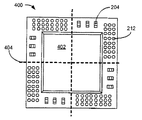
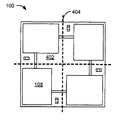
104 ディスクリート構成要素
106 モールドキャップ
108 オフセットパッケージ
110 切離し線
112 セクション
Claims (11)
- 集積回路パッケージオンパッケージ積層システムを製造する方法であって、
ベース基板を設けることと、
コンタクトパッドのアレイを前記ベース基板上に設けることと、
能動構成要素を前記ベース基板に取付けることと、
モールドキャップを前記ベース基板の中央部上に形成することと、
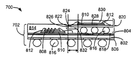
複数の上部パッケージを前記ベース基板の周縁部に沿うように前記ベース基板と前記モールドキャップに取付けることとを含み、前記モールドキャップの上部面の一部であって、前記ベース基板の周縁部側に位置する部分を露出したままにすることを含み、前記方法はさらに、
上部パッケージ間の前記モールドキャップと前記ベース基板とを切断することでパッケージオンパッケージを切離すことを含む、方法。 - 厚みの異なる部分を有するモールドキャップを前記ベース基板上に設けることをさらに含む、請求項1に記載の方法。
- 前記上部パッケージと前記モールドキャップの薄肉部との間に隙間充填剤を与えることをさらに含む、請求項1に記載の方法。
- 前記上部パッケージと前記ベース基板上のコンタクトパッドの前記アレイとの間にシステム相互接続部を設けることをさらに含む、請求項1に記載の方法。
- 前記モールドキャップと前記上部パッケージとの間にオーバーラップ領域を設けることをさらに含む、請求項1に記載の方法。
- 前記ベース基板上に厚みの異なる部分を有するモールドキャップを設けることをさらに含み、前記モールドキャップは、外周に薄肉部を含む、請求項1に記載の方法。
- 集積回路パッケージオンパッケージ積層システムであって、
ベース基板と、
前記ベース基板上のコンタクトパッドのアレイと、
前記ベース基板上の能動構成要素と、
前記ベース基板の一方端上のモールドキャップと、
前記ベース基板の一方端側に位置する前記モールドキャップの上部面を露出させ、前記ベース基板の他方端上および前記モールドキャップ上の上部パッケージとを含み、
前記モールドキャップは、厚みの異なる部分を含む、システム。 - 前記上部パッケージと前記モールドキャップの薄肉部との間に隙間充填剤をさらに含む、請求項7に記載のシステム。
- 前記上部パッケージと前記ベース基板上のコンタクトパッドの前記アレイとの間にシステム相互接続部をさらに含む、請求項7に記載のシステム。
- 前記モールドキャップと前記上部パッケージとの間にオーバーラップ領域をさらに含む、請求項7に記載のシステム。
- 前記モールドキャップは、厚みの異なる部分を含み、外周に薄肉部を含む、請求項7に記載のシステム。
Applications Claiming Priority (4)
| Application Number | Priority Date | Filing Date | Title |
|---|---|---|---|
| US59488705P | 2005-05-16 | 2005-05-16 | |
| US60/594,887 | 2005-05-16 | ||
| US11/383,407 US7746656B2 (en) | 2005-05-16 | 2006-05-15 | Offset integrated circuit package-on-package stacking system |
| US11/383,407 | 2006-05-15 |
Publications (3)
| Publication Number | Publication Date |
|---|---|
| JP2006324666A JP2006324666A (ja) | 2006-11-30 |
| JP2006324666A5 JP2006324666A5 (ja) | 2011-07-14 |
| JP5052037B2 true JP5052037B2 (ja) | 2012-10-17 |
Family
ID=37418900
Family Applications (1)
| Application Number | Title | Priority Date | Filing Date |
|---|---|---|---|
| JP2006136761A Active JP5052037B2 (ja) | 2005-05-16 | 2006-05-16 | オフセット集積回路パッケージオンパッケージ積層システム |
Country Status (4)
| Country | Link |
|---|---|
| US (1) | US7746656B2 (ja) |
| JP (1) | JP5052037B2 (ja) |
| KR (1) | KR101130330B1 (ja) |
| TW (1) | TWI381515B (ja) |
Families Citing this family (25)
| Publication number | Priority date | Publication date | Assignee | Title |
|---|---|---|---|---|
| JP4828202B2 (ja) * | 2005-10-20 | 2011-11-30 | ルネサスエレクトロニクス株式会社 | モジュール半導体装置 |
| JP2007116027A (ja) * | 2005-10-24 | 2007-05-10 | Elpida Memory Inc | 半導体装置の製造方法および半導体装置 |
| US8110899B2 (en) * | 2006-12-20 | 2012-02-07 | Intel Corporation | Method for incorporating existing silicon die into 3D integrated stack |
| US8043343B2 (en) * | 2007-06-28 | 2011-10-25 | Zimmer Spine, Inc. | Stabilization system and method |
| US7812435B2 (en) * | 2007-08-31 | 2010-10-12 | Stats Chippac Ltd. | Integrated circuit package-in-package system with side-by-side and offset stacking |
| US7872340B2 (en) * | 2007-08-31 | 2011-01-18 | Stats Chippac Ltd. | Integrated circuit package system employing an offset stacked configuration |
| US7985628B2 (en) * | 2007-12-12 | 2011-07-26 | Stats Chippac Ltd. | Integrated circuit package system with interconnect lock |
| US7781261B2 (en) * | 2007-12-12 | 2010-08-24 | Stats Chippac Ltd. | Integrated circuit package system with offset stacking and anti-flash structure |
| US8536692B2 (en) * | 2007-12-12 | 2013-09-17 | Stats Chippac Ltd. | Mountable integrated circuit package system with mountable integrated circuit die |
| US8084849B2 (en) * | 2007-12-12 | 2011-12-27 | Stats Chippac Ltd. | Integrated circuit package system with offset stacking |
| US8067828B2 (en) * | 2008-03-11 | 2011-11-29 | Stats Chippac Ltd. | System for solder ball inner stacking module connection |
| US20090243069A1 (en) * | 2008-03-26 | 2009-10-01 | Zigmund Ramirez Camacho | Integrated circuit package system with redistribution |
| CN101562952B (zh) * | 2008-04-18 | 2012-04-11 | 富葵精密组件(深圳)有限公司 | 线路基板、线路基板的制作方法及电路板的制作方法 |
| KR20100009055A (ko) * | 2008-07-17 | 2010-01-27 | 삼성전자주식회사 | 좁은 폭의 쏘우라인을 위한 인쇄회로기판 및 이를 포함하는반도체 패키지 |
| US9293385B2 (en) * | 2008-07-30 | 2016-03-22 | Stats Chippac Ltd. | RDL patterning with package on package system |
| US8406004B2 (en) * | 2008-12-09 | 2013-03-26 | Stats Chippac Ltd. | Integrated circuit packaging system and method of manufacture thereof |
| US7785925B2 (en) * | 2008-12-19 | 2010-08-31 | Stats Chippac Ltd. | Integrated circuit packaging system with package stacking and method of manufacture thereof |
| US7968995B2 (en) * | 2009-06-11 | 2011-06-28 | Stats Chippac Ltd. | Integrated circuit packaging system with package-on-package and method of manufacture thereof |
| US8518749B2 (en) | 2009-06-22 | 2013-08-27 | Stats Chippac, Ltd. | Semiconductor device and method of forming prefabricated heat spreader frame with embedded semiconductor die |
| US10163877B2 (en) * | 2011-11-07 | 2018-12-25 | Taiwan Semiconductor Manufacturing Co., Ltd. | System in package process flow |
| JP5979565B2 (ja) * | 2012-04-11 | 2016-08-24 | パナソニックIpマネジメント株式会社 | 半導体装置 |
| US9029234B2 (en) | 2012-05-15 | 2015-05-12 | International Business Machines Corporation | Physical design symmetry and integrated circuits enabling three dimentional (3D) yield optimization for wafer to wafer stacking |
| US9041176B2 (en) | 2012-10-08 | 2015-05-26 | Qualcomm Incorporated | Hybrid semiconductor module structure |
| KR20160123890A (ko) | 2015-04-17 | 2016-10-26 | 에스케이하이닉스 주식회사 | 검증용 인터포저 |
| JP2017022352A (ja) * | 2015-07-15 | 2017-01-26 | 富士通株式会社 | 半導体装置 |
Family Cites Families (40)
| Publication number | Priority date | Publication date | Assignee | Title |
|---|---|---|---|---|
| US5579207A (en) | 1994-10-20 | 1996-11-26 | Hughes Electronics | Three-dimensional integrated circuit stacking |
| JPH08222692A (ja) | 1995-02-09 | 1996-08-30 | Hitachi Ltd | 複合形半導体装置およびその実装構造体並びにその実装方法 |
| US5907903A (en) * | 1996-05-24 | 1999-06-01 | International Business Machines Corporation | Multi-layer-multi-chip pyramid and circuit board structure and method of forming same |
| US5748452A (en) | 1996-07-23 | 1998-05-05 | International Business Machines Corporation | Multi-electronic device package |
| US5986209A (en) | 1997-07-09 | 1999-11-16 | Micron Technology, Inc. | Package stack via bottom leaded plastic (BLP) packaging |
| JP3644662B2 (ja) | 1997-10-29 | 2005-05-11 | 株式会社ルネサステクノロジ | 半導体モジュール |
| JP2000208698A (ja) | 1999-01-18 | 2000-07-28 | Toshiba Corp | 半導体装置 |
| US6207474B1 (en) | 1998-03-09 | 2001-03-27 | Micron Technology, Inc. | Method of forming a stack of packaged memory die and resulting apparatus |
| US5854507A (en) | 1998-07-21 | 1998-12-29 | Hewlett-Packard Company | Multiple chip assembly |
| JP3767246B2 (ja) | 1999-05-26 | 2006-04-19 | 富士通株式会社 | 複合モジュール及びプリント回路基板ユニット |
| JP2001044362A (ja) | 1999-07-27 | 2001-02-16 | Mitsubishi Electric Corp | 半導体装置の実装構造および実装方法 |
| JP3798597B2 (ja) * | 1999-11-30 | 2006-07-19 | 富士通株式会社 | 半導体装置 |
| US6605875B2 (en) | 1999-12-30 | 2003-08-12 | Intel Corporation | Integrated circuit die having bond pads near adjacent sides to allow stacking of dice without regard to dice size |
| JP2001267473A (ja) * | 2000-03-17 | 2001-09-28 | Hitachi Ltd | 半導体装置およびその製造方法 |
| US6731009B1 (en) | 2000-03-20 | 2004-05-04 | Cypress Semiconductor Corporation | Multi-die assembly |
| US6518659B1 (en) | 2000-05-08 | 2003-02-11 | Amkor Technology, Inc. | Stackable package having a cavity and a lid for an electronic device |
| US6667544B1 (en) | 2000-06-30 | 2003-12-23 | Amkor Technology, Inc. | Stackable package having clips for fastening package and tool for opening clips |
| US7423336B2 (en) | 2002-04-08 | 2008-09-09 | Micron Technology, Inc. | Bond pad rerouting element, rerouted semiconductor devices including the rerouting element, and assemblies including the rerouted semiconductor devices |
| JP4601892B2 (ja) | 2002-07-04 | 2010-12-22 | ラムバス・インコーポレーテッド | 半導体装置および半導体チップのバンプ製造方法 |
| US20040021230A1 (en) | 2002-08-05 | 2004-02-05 | Macronix International Co., Ltd. | Ultra thin stacking packaging device |
| JP2004071947A (ja) | 2002-08-08 | 2004-03-04 | Renesas Technology Corp | 半導体装置 |
| KR100480437B1 (ko) * | 2002-10-24 | 2005-04-07 | 삼성전자주식회사 | 반도체 칩 패키지 적층 모듈 |
| US6798057B2 (en) | 2002-11-05 | 2004-09-28 | Micron Technology, Inc. | Thin stacked ball-grid array package |
| JP4110992B2 (ja) | 2003-02-07 | 2008-07-02 | セイコーエプソン株式会社 | 半導体装置、電子デバイス、電子機器、半導体装置の製造方法および電子デバイスの製造方法 |
| JP4408636B2 (ja) | 2003-02-28 | 2010-02-03 | 三洋電機株式会社 | 回路装置およびその製造方法 |
| JP4069771B2 (ja) * | 2003-03-17 | 2008-04-02 | セイコーエプソン株式会社 | 半導体装置、電子機器および半導体装置の製造方法 |
| TW576549U (en) | 2003-04-04 | 2004-02-11 | Advanced Semiconductor Eng | Multi-chip package combining wire-bonding and flip-chip configuration |
| US6853064B2 (en) * | 2003-05-12 | 2005-02-08 | Micron Technology, Inc. | Semiconductor component having stacked, encapsulated dice |
| JP3951966B2 (ja) | 2003-05-30 | 2007-08-01 | セイコーエプソン株式会社 | 半導体装置 |
| JP4324773B2 (ja) | 2003-09-24 | 2009-09-02 | セイコーエプソン株式会社 | 半導体装置の製造方法 |
| US7030469B2 (en) * | 2003-09-25 | 2006-04-18 | Freescale Semiconductor, Inc. | Method of forming a semiconductor package and structure thereof |
| JP2005123463A (ja) * | 2003-10-17 | 2005-05-12 | Seiko Epson Corp | 半導体装置及びその製造方法、半導体装置モジュール、回路基板並びに電子機器 |
| US7095104B2 (en) | 2003-11-21 | 2006-08-22 | International Business Machines Corporation | Overlap stacking of center bus bonded memory chips for double density and method of manufacturing the same |
| US7091581B1 (en) * | 2004-06-14 | 2006-08-15 | Asat Limited | Integrated circuit package and process for fabricating the same |
| JP2006186136A (ja) * | 2004-12-28 | 2006-07-13 | Toshiba Corp | 両面部品実装回路基板及びその製造方法 |
| US7312519B2 (en) | 2006-01-12 | 2007-12-25 | Stats Chippac Ltd. | Stacked integrated circuit package-in-package system |
| US7420269B2 (en) | 2006-04-18 | 2008-09-02 | Stats Chippac Ltd. | Stacked integrated circuit package-in-package system |
| US7535086B2 (en) * | 2006-08-03 | 2009-05-19 | Stats Chippac Ltd. | Integrated circuit package-on-package stacking system |
| US7772683B2 (en) | 2006-12-09 | 2010-08-10 | Stats Chippac Ltd. | Stacked integrated circuit package-in-package system |
| US7635913B2 (en) | 2006-12-09 | 2009-12-22 | Stats Chippac Ltd. | Stacked integrated circuit package-in-package system |
-
2006
- 2006-05-15 US US11/383,407 patent/US7746656B2/en active Active
- 2006-05-16 KR KR1020060043995A patent/KR101130330B1/ko active IP Right Grant
- 2006-05-16 JP JP2006136761A patent/JP5052037B2/ja active Active
- 2006-05-16 TW TW095117222A patent/TWI381515B/zh active
Also Published As
| Publication number | Publication date |
|---|---|
| TW200707700A (en) | 2007-02-16 |
| KR101130330B1 (ko) | 2012-03-26 |
| US7746656B2 (en) | 2010-06-29 |
| TWI381515B (zh) | 2013-01-01 |
| KR20060118364A (ko) | 2006-11-23 |
| US20060256525A1 (en) | 2006-11-16 |
| JP2006324666A (ja) | 2006-11-30 |
Similar Documents
| Publication | Publication Date | Title |
|---|---|---|
| JP5052037B2 (ja) | オフセット集積回路パッケージオンパッケージ積層システム | |
| JP2006324666A5 (ja) | ||
| JP4402074B2 (ja) | オフセット集積回路パッケージオンパッケージ積層システムおよびその製造方法 | |
| US7388280B2 (en) | Package stacking lead frame system | |
| US8232658B2 (en) | Stackable integrated circuit package system with multiple interconnect interface | |
| US6861288B2 (en) | Stacked semiconductor packages and method for the fabrication thereof | |
| US8541872B2 (en) | Integrated circuit package system with package stacking and method of manufacture thereof | |
| TWI499032B (zh) | 積體電路層疊封裝件堆疊系統 | |
| US8729687B2 (en) | Stackable integrated circuit package system | |
| US8633100B2 (en) | Method of manufacturing integrated circuit packaging system with support structure | |
| US7915724B2 (en) | Integrated circuit packaging system with base structure device | |
| US8247894B2 (en) | Integrated circuit package system with step mold recess | |
| US20070001296A1 (en) | Bump for overhang device | |
| US8124451B2 (en) | Integrated circuit packaging system with interposer | |
| US20110089552A1 (en) | Integrated circuit packaging system with package-on-package stacking and method of manufacture thereof | |
| TWI430425B (zh) | 採用凸塊技術之積體電路封裝件系統 | |
| US20080029867A1 (en) | Stackable multi-chip package system | |
| US7656017B2 (en) | Integrated circuit package system with thermo-mechanical interlocking substrates | |
| US20090236704A1 (en) | Integrated circuit package system with isolated leads | |
| US8847413B2 (en) | Integrated circuit package system with leads having multiple sides exposed | |
| US7759783B2 (en) | Integrated circuit package system employing thin profile techniques | |
| US20080315406A1 (en) | Integrated circuit package system with cavity substrate | |
| US8062934B2 (en) | Integrated circuit package system with ground bonds | |
| US8269324B2 (en) | Integrated circuit package system with chip on lead |
Legal Events
| Date | Code | Title | Description |
|---|---|---|---|
| A521 | Request for written amendment filed |
Free format text: JAPANESE INTERMEDIATE CODE: A523 Effective date: 20090428 |
|
| A621 | Written request for application examination |
Free format text: JAPANESE INTERMEDIATE CODE: A621 Effective date: 20090428 |
|
| A521 | Request for written amendment filed |
Free format text: JAPANESE INTERMEDIATE CODE: A523 Effective date: 20110525 |
|
| A871 | Explanation of circumstances concerning accelerated examination |
Free format text: JAPANESE INTERMEDIATE CODE: A871 Effective date: 20110525 |
|
| A977 | Report on retrieval |
Free format text: JAPANESE INTERMEDIATE CODE: A971007 Effective date: 20110726 |
|
| A975 | Report on accelerated examination |
Free format text: JAPANESE INTERMEDIATE CODE: A971005 Effective date: 20110726 |
|
| A131 | Notification of reasons for refusal |
Free format text: JAPANESE INTERMEDIATE CODE: A131 Effective date: 20110809 |
|
| A521 | Request for written amendment filed |
Free format text: JAPANESE INTERMEDIATE CODE: A523 Effective date: 20111108 |
|
| A02 | Decision of refusal |
Free format text: JAPANESE INTERMEDIATE CODE: A02 Effective date: 20111206 |
|
| A521 | Request for written amendment filed |
Free format text: JAPANESE INTERMEDIATE CODE: A523 Effective date: 20120405 |
|
| A911 | Transfer to examiner for re-examination before appeal (zenchi) |
Free format text: JAPANESE INTERMEDIATE CODE: A911 Effective date: 20120521 |
|
| TRDD | Decision of grant or rejection written | ||
| A01 | Written decision to grant a patent or to grant a registration (utility model) |
Free format text: JAPANESE INTERMEDIATE CODE: A01 Effective date: 20120703 |
|
| A01 | Written decision to grant a patent or to grant a registration (utility model) |
Free format text: JAPANESE INTERMEDIATE CODE: A01 |
|
| A61 | First payment of annual fees (during grant procedure) |
Free format text: JAPANESE INTERMEDIATE CODE: A61 Effective date: 20120724 |
|
| R150 | Certificate of patent or registration of utility model |
Free format text: JAPANESE INTERMEDIATE CODE: R150 Ref document number: 5052037 Country of ref document: JP Free format text: JAPANESE INTERMEDIATE CODE: R150 |
|
| FPAY | Renewal fee payment (event date is renewal date of database) |
Free format text: PAYMENT UNTIL: 20150803 Year of fee payment: 3 |
|
| R250 | Receipt of annual fees |
Free format text: JAPANESE INTERMEDIATE CODE: R250 |
|
| R250 | Receipt of annual fees |
Free format text: JAPANESE INTERMEDIATE CODE: R250 |
|
| R250 | Receipt of annual fees |
Free format text: JAPANESE INTERMEDIATE CODE: R250 |
|
| R250 | Receipt of annual fees |
Free format text: JAPANESE INTERMEDIATE CODE: R250 |
|
| R250 | Receipt of annual fees |
Free format text: JAPANESE INTERMEDIATE CODE: R250 |
|
| R250 | Receipt of annual fees |
Free format text: JAPANESE INTERMEDIATE CODE: R250 |
|
| R250 | Receipt of annual fees |
Free format text: JAPANESE INTERMEDIATE CODE: R250 |
|
| R250 | Receipt of annual fees |
Free format text: JAPANESE INTERMEDIATE CODE: R250 |
|
| R250 | Receipt of annual fees |
Free format text: JAPANESE INTERMEDIATE CODE: R250 |