US7812435B2 - Integrated circuit package-in-package system with side-by-side and offset stacking - Google Patents
Integrated circuit package-in-package system with side-by-side and offset stacking Download PDFInfo
- Publication number
- US7812435B2 US7812435B2 US11/849,087 US84908707A US7812435B2 US 7812435 B2 US7812435 B2 US 7812435B2 US 84908707 A US84908707 A US 84908707A US 7812435 B2 US7812435 B2 US 7812435B2
- Authority
- US
- United States
- Prior art keywords
- integrated circuit
- circuit device
- substrate
- package system
- over
- Prior art date
- Legal status (The legal status is an assumption and is not a legal conclusion. Google has not performed a legal analysis and makes no representation as to the accuracy of the status listed.)
- Active, expires
Links
Images


Classifications
-
- H—ELECTRICITY
- H10—SEMICONDUCTOR DEVICES; ELECTRIC SOLID-STATE DEVICES NOT OTHERWISE PROVIDED FOR
- H10W—GENERIC PACKAGES, INTERCONNECTIONS, CONNECTORS OR OTHER CONSTRUCTIONAL DETAILS OF DEVICES COVERED BY CLASS H10
- H10W74/00—Encapsulations, e.g. protective coatings
- H10W74/10—Encapsulations, e.g. protective coatings characterised by their shape or disposition
- H10W74/111—Encapsulations, e.g. protective coatings characterised by their shape or disposition the semiconductor body being completely enclosed
- H10W74/114—Encapsulations, e.g. protective coatings characterised by their shape or disposition the semiconductor body being completely enclosed by a substrate and the encapsulations
- H10W74/117—Encapsulations, e.g. protective coatings characterised by their shape or disposition the semiconductor body being completely enclosed by a substrate and the encapsulations the substrate having spherical bumps for external connection
-
- H—ELECTRICITY
- H10—SEMICONDUCTOR DEVICES; ELECTRIC SOLID-STATE DEVICES NOT OTHERWISE PROVIDED FOR
- H10W—GENERIC PACKAGES, INTERCONNECTIONS, CONNECTORS OR OTHER CONSTRUCTIONAL DETAILS OF DEVICES COVERED BY CLASS H10
- H10W90/00—Package configurations
-
- H—ELECTRICITY
- H10—SEMICONDUCTOR DEVICES; ELECTRIC SOLID-STATE DEVICES NOT OTHERWISE PROVIDED FOR
- H10W—GENERIC PACKAGES, INTERCONNECTIONS, CONNECTORS OR OTHER CONSTRUCTIONAL DETAILS OF DEVICES COVERED BY CLASS H10
- H10W72/00—Interconnections or connectors in packages
- H10W72/50—Bond wires
- H10W72/531—Shapes of wire connectors
- H10W72/533—Cross-sectional shape
- H10W72/534—Cross-sectional shape being rectangular
-
- H—ELECTRICITY
- H10—SEMICONDUCTOR DEVICES; ELECTRIC SOLID-STATE DEVICES NOT OTHERWISE PROVIDED FOR
- H10W—GENERIC PACKAGES, INTERCONNECTIONS, CONNECTORS OR OTHER CONSTRUCTIONAL DETAILS OF DEVICES COVERED BY CLASS H10
- H10W72/00—Interconnections or connectors in packages
- H10W72/851—Dispositions of multiple connectors or interconnections
- H10W72/874—On different surfaces
- H10W72/877—Bump connectors and die-attach connectors
-
- H—ELECTRICITY
- H10—SEMICONDUCTOR DEVICES; ELECTRIC SOLID-STATE DEVICES NOT OTHERWISE PROVIDED FOR
- H10W—GENERIC PACKAGES, INTERCONNECTIONS, CONNECTORS OR OTHER CONSTRUCTIONAL DETAILS OF DEVICES COVERED BY CLASS H10
- H10W72/00—Interconnections or connectors in packages
- H10W72/851—Dispositions of multiple connectors or interconnections
- H10W72/874—On different surfaces
- H10W72/884—Die-attach connectors and bond wires
-
- H—ELECTRICITY
- H10—SEMICONDUCTOR DEVICES; ELECTRIC SOLID-STATE DEVICES NOT OTHERWISE PROVIDED FOR
- H10W—GENERIC PACKAGES, INTERCONNECTIONS, CONNECTORS OR OTHER CONSTRUCTIONAL DETAILS OF DEVICES COVERED BY CLASS H10
- H10W74/00—Encapsulations, e.g. protective coatings
-
- H—ELECTRICITY
- H10—SEMICONDUCTOR DEVICES; ELECTRIC SOLID-STATE DEVICES NOT OTHERWISE PROVIDED FOR
- H10W—GENERIC PACKAGES, INTERCONNECTIONS, CONNECTORS OR OTHER CONSTRUCTIONAL DETAILS OF DEVICES COVERED BY CLASS H10
- H10W90/00—Package configurations
- H10W90/20—Configurations of stacked chips
- H10W90/24—Configurations of stacked chips at least one of the stacked chips being laterally offset from a neighbouring stacked chip, e.g. chip stacks having a staircase shape
-
- H—ELECTRICITY
- H10—SEMICONDUCTOR DEVICES; ELECTRIC SOLID-STATE DEVICES NOT OTHERWISE PROVIDED FOR
- H10W—GENERIC PACKAGES, INTERCONNECTIONS, CONNECTORS OR OTHER CONSTRUCTIONAL DETAILS OF DEVICES COVERED BY CLASS H10
- H10W90/00—Package configurations
- H10W90/701—Package configurations characterised by the relative positions of pads or connectors relative to package parts
- H10W90/721—Package configurations characterised by the relative positions of pads or connectors relative to package parts of bump connectors
- H10W90/722—Package configurations characterised by the relative positions of pads or connectors relative to package parts of bump connectors between stacked chips
-
- H—ELECTRICITY
- H10—SEMICONDUCTOR DEVICES; ELECTRIC SOLID-STATE DEVICES NOT OTHERWISE PROVIDED FOR
- H10W—GENERIC PACKAGES, INTERCONNECTIONS, CONNECTORS OR OTHER CONSTRUCTIONAL DETAILS OF DEVICES COVERED BY CLASS H10
- H10W90/00—Package configurations
- H10W90/701—Package configurations characterised by the relative positions of pads or connectors relative to package parts
- H10W90/721—Package configurations characterised by the relative positions of pads or connectors relative to package parts of bump connectors
- H10W90/724—Package configurations characterised by the relative positions of pads or connectors relative to package parts of bump connectors between a chip and a stacked insulating package substrate, interposer or RDL
-
- H—ELECTRICITY
- H10—SEMICONDUCTOR DEVICES; ELECTRIC SOLID-STATE DEVICES NOT OTHERWISE PROVIDED FOR
- H10W—GENERIC PACKAGES, INTERCONNECTIONS, CONNECTORS OR OTHER CONSTRUCTIONAL DETAILS OF DEVICES COVERED BY CLASS H10
- H10W90/00—Package configurations
- H10W90/701—Package configurations characterised by the relative positions of pads or connectors relative to package parts
- H10W90/731—Package configurations characterised by the relative positions of pads or connectors relative to package parts of die-attach connectors
- H10W90/732—Package configurations characterised by the relative positions of pads or connectors relative to package parts of die-attach connectors between stacked chips
-
- H—ELECTRICITY
- H10—SEMICONDUCTOR DEVICES; ELECTRIC SOLID-STATE DEVICES NOT OTHERWISE PROVIDED FOR
- H10W—GENERIC PACKAGES, INTERCONNECTIONS, CONNECTORS OR OTHER CONSTRUCTIONAL DETAILS OF DEVICES COVERED BY CLASS H10
- H10W90/00—Package configurations
- H10W90/701—Package configurations characterised by the relative positions of pads or connectors relative to package parts
- H10W90/751—Package configurations characterised by the relative positions of pads or connectors relative to package parts of bond wires
- H10W90/754—Package configurations characterised by the relative positions of pads or connectors relative to package parts of bond wires between a chip and a stacked insulating package substrate, interposer or RDL
Definitions
- the present invention relates generally to an integrated circuit package system and more particularly to an integrated circuit package-in-package system.
- Modern electronics such as smart phones, personal digital assistants, location based services devices, servers, and storage arrays, are packing more integrated circuits into an ever-shrinking physical space with expectations for decreasing cost.
- Numerous technologies have been developed to meet these requirements. Some of the research and development strategies focus on new package technologies while others focus on improving the existing package technologies. Research and development in the existing package technologies may take a myriad of different directions.
- Multi-chip packages whether vertically or horizontally arranged, can also present problems because they usually must be assembled before the integrated circuit and integrated circuit connections can be tested.
- integrated circuits are mounted and connected in a multi-chip module, individual integrated circuits and connections cannot be tested individually, and it is not possible to identify known-good-die (“KGD”) before being assembled into larger circuits. Consequently, conventional multi-chip packages lead to assembly process yield problems. This fabrication process, which does not identify KGD, is therefore less reliable and more prone to assembly defects.
- multi-chip packages provide integration solutions for packing more integrated circuits and components into a single package.
- market driven requirements continue to drive conventional multi-chip packages to smaller and smaller form factors.
- the present invention provides an integrated circuit package-in-package system including: mounting a first integrated circuit device over a substrate; mounting an integrated circuit package system having an inner encapsulation over the first integrated circuit device with a first offset; mounting a second integrated circuit device over the first integrated circuit device and adjacent to the integrated circuit package system; connecting the integrated circuit package system and the substrate; and forming a package encapsulation as a cover for the first integrated circuit device, the integrated circuit package system, and the second integrated circuit device.
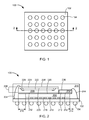
- FIG. 1 is a bottom view of an integrated circuit package-in-package system in a first embodiment of the present invention
- FIG. 2 is a cross-sectional view of the integrated circuit package-in-package system along line 2 - 2 of FIG. 1 ;
- FIG. 3 is a cross-sectional view of an integrated circuit package-in-package system exemplified by the top view of FIG. 1 in a second embodiment of the present invention
- FIG. 4 is a cross-sectional view of an integrated circuit package-in-package system exemplified by the top view of FIG. 1 in a third embodiment of the present invention
- FIG. 5 is a cross-sectional view of an integrated circuit package-in-package system exemplified by the top view of FIG. 1 in a fourth embodiment of the present invention.
- FIG. 6 is a flow chart of an integrated circuit package-in-package system for manufacturing of the integrated circuit package-in-package system in an embodiment of the present invention.
- the term “horizontal” as used herein is defined as a plane parallel to the plane or surface of the integrated circuit, regardless of its orientation.
- the term “vertical” refers to a direction perpendicular to the horizontal as just defined. Terms, such as “above”, “below”, “bottom”, “top”, “side” (as in “sidewall”), “higher”, “lower”, “upper”, “over”, and “under”, are defined with respect to the horizontal plane.
- the term “on” means there is direct contact among elements.
- processing as used herein includes deposition of material, patterning, exposure, development, etching, cleaning, molding, and/or removal of the material or as required in forming a described structure.
- system as used herein means and refers to the method and to the apparatus of the present invention in accordance with the context in which the term is used.
- FIG. 1 therein is shown a bottom view of an integrated circuit package-in-package system 100 in a first embodiment of the present invention.
- the bottom view depicts a substrate 102 , such as a laminated plastic or ceramic substrate, with external interconnects 104 , such as solder balls, preferably attached to the substrate 102 .
- the external interconnects 104 are shown in an array configuration, although it is understood that the external interconnects 104 may populate the substrate 102 in a different configuration. For example, the external interconnects 104 may not populate all the locations of the array configuration.
- FIG. 2 therein is shown a cross-sectional view of the integrated circuit package-in-package system 100 along line 2 - 2 of FIG. 1 .
- the external interconnects 104 are preferably attached below the substrate 102 .
- a first integrated circuit device 206 preferably mounts over the substrate 102 .
- An integrated circuit package system 208 preferably mounts over the first integrated circuit device 206 , wherein the integrated circuit package system 208 is shown, as an example, with a first offset 210 from the edge of the first integrated circuit device 206 .
- a second integrated circuit device 212 is preferably adjacent, such as side-by-side, to the integrated circuit package system 208 and over the first integrated circuit device 206 .
- the second integrated circuit device 212 is shown, as an example, with a second offset 214 from a different edge of the first integrated circuit device 206 .
- the first integrated circuit device 206 is shown as a flip chip having electrical connectors 216 , such as solder bumps, at a first active side 218 of the first integrated circuit device 206 , wherein the first active side 218 includes active circuitry (not shown) fabricated thereon.
- the first active side 218 faces the substrate 102 with the electrical connectors 216 connected between the first active side 218 and the substrate 102 .
- the first integrated circuit device 206 also includes a first non-active side 220 at an opposing side of the first active side 218 .
- the integrated circuit package system 208 includes an integrated circuit die 222 preferably mounted to a carrier 224 , such as a substrate or interposer.
- Inner interconnects 226 such as bond wires or ribbon bond wires, connect the integrated circuit die 222 and a first side 228 of the carrier 224 .
- An inner encapsulation 230 such as an epoxy molding compound, covers the integrated circuit die 222 , the inner interconnects 226 , and the first side 228 of the carrier 224 .
- the integrated circuit package system 208 preferably mounts over the first integrated circuit device 206 with a first adhesive 232 , such as a film adhesive, between the inner encapsulation 230 and the first non-active side 220 .
- the first adhesive 232 is also shown along the horizontal portion of the inner encapsulation 230 at the first offset 210 .
- First internal interconnects 234 such as bond wires or ribbon bond wires, preferably connect between a second side 236 of the carrier 224 and the substrate 102 , wherein the second side 236 is at an opposing side to the first side 228 .
- the second integrated circuit device 212 is shown as an integrated circuit die having a second active side 238 and a second non-active side 240 , wherein the second active side 238 includes active circuitry (not shown) fabricated thereon.
- the second integrated circuit device 212 preferably mounts over the first integrated circuit device 206 with a second adhesive 242 , such as a die-attach adhesive, between the second non-active side 240 and the first non-active side 220 .
- the second adhesive 242 is also shown along the second non-active side 240 at the second offset 214 .
- the first adhesive 232 and the second adhesive 242 may include substantially the same materials or may be different.
- Second internal interconnects 244 such as bond wires or ribbon bond wires, may connect between the second active side 238 and the substrate 102 .
- a package encapsulation 246 such as an epoxy molding compound, covers the first integrated circuit device 206 , the integrated circuit package system 208 , the second integrated circuit device 212 , the first internal interconnects 234 , and the second internal interconnects 244 over the substrate 102 .
- the package encapsulation 246 preferably fills the space underneath the first offset 210 and the second offset 214 .
- FIG. 3 therein is shown a cross-sectional view of an integrated circuit package-in-package system 300 exemplified by the top view of FIG. 1 in a second embodiment of the present invention.
- External interconnects 304 such as solder balls, are preferably attached below a substrate 302 , such as a plastic or ceramic substrate.
- a first integrated circuit device 306 preferably mounts over the substrate 302 .
- An integrated circuit package system 308 preferably mounts over the first integrated circuit device 306 , wherein the integrated circuit package system 308 is shown, as an example, with a first offset 310 from the edge of the first integrated circuit device 306 .
- a second integrated circuit device 312 is preferably adjacent, such as side-by-side, to the integrated circuit package system 308 and over the first integrated circuit device 306 .
- the second integrated circuit device 312 is shown, as an example, with a second offset 314 from a different edge of the first integrated circuit device 306 .
- the first integrated circuit device 306 is shown as a flip chip having electrical connectors 316 , such as solder bumps, at a first active side 318 of the first integrated circuit device 306 , wherein the first active side 318 includes active circuitry (not shown) fabricated thereon.
- the first active side 318 faces the substrate 302 with the electrical connectors 316 connected between the first active side 318 and the substrate 302 .
- the first integrated circuit device 306 also includes a first non-active side 320 at an opposing side of the first active side 318 .
- the integrated circuit package system 308 includes an integrated circuit die 322 preferably mounted to a carrier 324 , such as a substrate or interposer.
- Inner interconnects 326 such as bond wires or ribbon bond wires, connect the integrated circuit die 322 and a first side 328 of the carrier 324 .
- An inner encapsulation 330 such as an epoxy molding compound, covers the integrated circuit die 322 , the inner interconnects 326 , and the first side 328 of the carrier 324 .
- the integrated circuit package system 308 preferably mounts over the first integrated circuit device 306 with a first adhesive 332 , such as a film adhesive, between the inner encapsulation 330 and the first non-active side 320 .
- a support structure 350 such as an epoxy film or a passive component, preferably supports the integrated circuit package system 308 at the first offset 310 .
- the support structure 350 is adjacent to the first integrated circuit device 306 and has substantially the same or similar height to the first integrated circuit device 306 from the substrate 302 .
- the first adhesive 332 is sufficiently malleable to mitigate or accommodate minor height differences between the first integrated circuit device 306 and the support structure 350 .
- the first adhesive 332 is also shown along the horizontal portion of the inner encapsulation 330 at the first offset 310 and also between the inner encapsulation 330 and the support structure 350 .
- First internal interconnects 334 such as bond wires or ribbon bond wires, preferably connect between a second side 336 of the carrier 324 and the substrate 302 , wherein the second side 336 is at an opposing side to the first side 328 .
- the second integrated circuit device 312 is shown as an integrated circuit die having a second active side 338 and a second non-active side 340 , wherein the second active side 338 includes active circuitry (not shown) fabricated thereon.
- the second integrated circuit device 312 preferably mounts over the first integrated circuit device 306 with a second adhesive 342 , such as a die-attach adhesive, between the second non-active side 340 and the first non-active side 320 .
- the second adhesive 342 is also shown along the second non-active side 340 at the second offset 314 .
- the first adhesive 332 and the second adhesive 342 may include substantially the same materials or may be different.
- Second internal interconnects 344 such as bond wires or ribbon bond wires, may connect between the second active side 338 and the substrate 302 .
- a package encapsulation 346 such as an epoxy molding compound, covers the first integrated circuit device 306 , the integrated circuit package system 308 , the second integrated circuit device 312 , the first internal interconnects 334 , and the second internal interconnects 344 over the substrate 302 .
- the package encapsulation 346 preferably fills the space underneath the first offset 310 and the second offset 314 .
- FIG. 4 therein is shown a cross-sectional view of an integrated circuit package-in-package system 400 exemplified by the top view of FIG. 1 in a third embodiment of the present invention.
- External interconnects 404 such as solder balls, are preferably attached below a substrate 402 , such as a plastic or ceramic substrate.
- a first integrated circuit device 406 preferably mounts over the substrate 402 .
- An integrated circuit package system 408 preferably mounts over the first integrated circuit device 406 , wherein the integrated circuit package system 408 is shown, as an example, with a first offset 410 from the edge of the first integrated circuit device 406 .
- a second integrated circuit device 412 is preferably adjacent, such as side-by-side, to the integrated circuit package system 408 and over the first integrated circuit device 406 .
- the first integrated circuit device 406 is shown as a flip chip having electrical connectors 416 , such as solder bumps, at a first active side 418 of the first integrated circuit device 406 , wherein the first active side 418 includes active circuitry (not shown) fabricated thereon.
- the first active side 418 faces the substrate 402 with the electrical connectors 416 connected between the first active side 418 and the substrate 402 .
- the first integrated circuit device 406 also includes a first non-active side 420 at an opposing side of the first active side 418 .
- the integrated circuit package system 408 includes an integrated circuit die 422 preferably mounted to a carrier 424 , such as a substrate or interposer.
- Inner interconnects 426 such as bond wires or ribbon bond wires, connect the integrated circuit die 422 and a first side 428 of the carrier 424 .
- An inner encapsulation 430 such as an epoxy molding compound, covers the integrated circuit die 422 , the inner interconnects 426 , and the first side 428 of the carrier 424 .
- the integrated circuit package system 408 preferably mounts over the first integrated circuit device 406 with a first adhesive 432 , such as a film adhesive, between the inner encapsulation 430 and the first non-active side 420 .
- a support structure 450 such as an epoxy film or a passive component, preferably supports the integrated circuit package system 408 at the first offset 410 .
- the support structure 450 is adjacent to the first integrated circuit device 406 and has substantially the same or similar height to the first integrated circuit device 406 from the substrate 402 .
- the first adhesive 432 is sufficiently malleable to mitigate or accommodate minor height differences between the first integrated circuit device 406 and the support structure 450 .
- the first adhesive 432 is also shown along the horizontal portion of the inner encapsulation 430 at the first offset 410 and also between the inner encapsulation 430 and the support structure 450 .
- First internal interconnects 434 such as bond wires or ribbon bond wires, preferably connect between a second side 436 of the carrier 424 and the substrate 402 , wherein the second side 436 is at an opposing side to the first side 428 .
- the second integrated circuit device 412 is shown as an integrated circuit die having a second active side 438 and a second non-active side 440 , wherein the second active side 438 includes active circuitry (not shown) fabricated thereon.
- the second integrated circuit device 412 preferably mounts over the first integrated circuit device 406 with the second active side 438 facing the first non-active side 420 .
- Second internal interconnects 444 may connect between the second active side 438 and the first non-active side 420 , wherein the second internal interconnects 444 preferably attach to terminals (not shown) exposed at the first non-active side 420 .
- the terminals at the first non-active side 420 preferably connect to the first active side 418 with vias (not shown) through the first integrated circuit device 406 .
- a package encapsulation 446 such as an epoxy molding compound, covers the first integrated circuit device 406 , the integrated circuit package system 408 , the second integrated circuit device 412 , the first internal interconnects 434 , and the second internal interconnects 444 over the substrate 402 .
- the package encapsulation 446 preferably fills the space underneath the first offset 410 .
- FIG. 5 therein is shown a cross-sectional view of an integrated circuit package-in-package system 500 exemplified by the top view of FIG. 1 in a fourth embodiment of the present invention.
- External interconnects 504 such as solder balls, are preferably attached below a substrate 502 , such as a plastic or ceramic substrate.
- a first integrated circuit device 506 preferably mounts over the substrate 502 .
- An integrated circuit package system 508 preferably mounts over the first integrated circuit device 506 , wherein the integrated circuit package system 508 is shown, as an example, with a first offset 510 from the edge of the first integrated circuit device 506 .
- a second integrated circuit device 512 is preferably adjacent, such as side-by-side, to the integrated circuit package system 508 and over the first integrated circuit device 506 .
- the first integrated circuit device 506 is shown as a flip chip having electrical connectors 516 , such as solder bumps, at a first active side 518 of the first integrated circuit device 506 , wherein the first active side 518 includes active circuitry (not shown) fabricated thereon.
- the first active side 518 faces the substrate 502 with the electrical connectors 516 connected between the first active side 518 and the substrate 502 .
- the first integrated circuit device 506 also includes a first non-active side 520 at an opposing side of the first active side 518 .
- the integrated circuit package system 508 includes an integrated circuit die 522 preferably mounted to a carrier 524 , such as a substrate or interposer.
- Inner interconnects 526 such as bond wires or ribbon bond wires, connect the integrated circuit die 522 and a first side 528 of the carrier 524 .
- An inner encapsulation 530 such as an epoxy molding compound, covers the integrated circuit die 522 , the inner interconnects 526 , and the first side 528 of the carrier 524 .
- the integrated circuit package system 508 preferably mounts over the first integrated circuit device 506 with a second side 536 of the carrier 524 facing the first non-active side 520 , wherein the second side 536 is at an opposing side to the first side 528 .
- First internal interconnects 534 such as solder balls, preferably connects the second side 536 and the substrate 502 at the first offset 510 .
- the first internal interconnects 534 also supports the integrated circuit package system 508 at the first offset 510 .
- the first internal interconnects 534 is adjacent to the first integrated circuit device 506 and has substantially the same or similar height to the first integrated circuit device 506 from the substrate 502 .
- the second integrated circuit device 512 is shown as an integrated circuit die having a second active side 538 and a second non-active side 540 , wherein the second active side 538 includes active circuitry (not shown) fabricated thereon.
- the second integrated circuit device 512 preferably mounts over the first integrated circuit device 506 with the second active side 538 facing the first non-active side 520 .
- Second internal interconnects 544 may connect between the second active side 538 and the first non-active side 520 , wherein the second internal interconnects 544 preferably attach to terminals (not shown) exposed at the first non-active side 520 .
- the terminals at the first non-active side 520 preferably connect to the first active side 518 with vias (not shown) through the first integrated circuit device 506 .
- a package encapsulation 546 such as an epoxy molding compound, covers the first integrated circuit device 506 , the second integrated circuit device 512 , the first internal interconnects 534 , and the second internal interconnects 544 over the substrate 502 .
- the package encapsulation 546 partially covers the integrated circuit package system 508 exposing the inner encapsulation 530 minimizing the height of the integrated circuit package-in-package system 500 .
- the package encapsulation 546 preferably fills the space underneath the first offset 510 .
- FIG. 6 therein is shown a flow chart of an integrated circuit package-in-package system 600 for manufacturing the integrated circuit package-in-package system 100 in an embodiment of the present invention.
- the system 600 includes mounting a first integrated circuit device over a substrate in a block 602 ; mounting an integrated circuit package system having an inner encapsulation over the first integrated circuit device with a first offset in a block 604 ; mounting a second integrated circuit device over the first integrated circuit device and adjacent to the integrated circuit package system in a block 606 ; connecting the integrated circuit package system and the substrate in a block 608 ; and forming a package encapsulation as a cover for the first integrated circuit device, the integrated circuit package system, and the second integrated circuit device in a block 610 .
- Yet another important aspect of the present invention is that it valuably supports and services the historical trend of reducing costs, simplifying systems, and increasing performance.
- the integrated circuit package-in-package system of the present invention furnishes important and heretofore unknown and unavailable solutions, capabilities, and functional aspects for improving yield, increasing reliability, and reducing cost of circuit system.
- the resulting processes and configurations are straightforward, cost-effective, uncomplicated, highly versatile, accurate, sensitive, and effective, and can be implemented by adapting known components for ready, efficient, and economical manufacturing, application, and utilization.
Landscapes
- Structures Or Materials For Encapsulating Or Coating Semiconductor Devices Or Solid State Devices (AREA)
Abstract
Description
Claims (17)
Priority Applications (2)
| Application Number | Priority Date | Filing Date | Title |
|---|---|---|---|
| US11/849,087 US7812435B2 (en) | 2007-08-31 | 2007-08-31 | Integrated circuit package-in-package system with side-by-side and offset stacking |
| US12/871,031 US8093727B2 (en) | 2007-08-31 | 2010-08-30 | Integrated circuit package-in-package system with side-by-side and offset stacking and method for manufacturing thereof |
Applications Claiming Priority (1)
| Application Number | Priority Date | Filing Date | Title |
|---|---|---|---|
| US11/849,087 US7812435B2 (en) | 2007-08-31 | 2007-08-31 | Integrated circuit package-in-package system with side-by-side and offset stacking |
Related Child Applications (1)
| Application Number | Title | Priority Date | Filing Date |
|---|---|---|---|
| US12/871,031 Continuation US8093727B2 (en) | 2007-08-31 | 2010-08-30 | Integrated circuit package-in-package system with side-by-side and offset stacking and method for manufacturing thereof |
Publications (2)
| Publication Number | Publication Date |
|---|---|
| US20090057861A1 US20090057861A1 (en) | 2009-03-05 |
| US7812435B2 true US7812435B2 (en) | 2010-10-12 |
Family
ID=40406119
Family Applications (2)
| Application Number | Title | Priority Date | Filing Date |
|---|---|---|---|
| US11/849,087 Active 2029-01-18 US7812435B2 (en) | 2007-08-31 | 2007-08-31 | Integrated circuit package-in-package system with side-by-side and offset stacking |
| US12/871,031 Active US8093727B2 (en) | 2007-08-31 | 2010-08-30 | Integrated circuit package-in-package system with side-by-side and offset stacking and method for manufacturing thereof |
Family Applications After (1)
| Application Number | Title | Priority Date | Filing Date |
|---|---|---|---|
| US12/871,031 Active US8093727B2 (en) | 2007-08-31 | 2010-08-30 | Integrated circuit package-in-package system with side-by-side and offset stacking and method for manufacturing thereof |
Country Status (1)
| Country | Link |
|---|---|
| US (2) | US7812435B2 (en) |
Cited By (1)
| Publication number | Priority date | Publication date | Assignee | Title |
|---|---|---|---|---|
| US20100314736A1 (en) * | 2009-06-11 | 2010-12-16 | Chan Hoon Ko | Integrated circuit packaging system with package-on-package and method of manufacture thereof |
Families Citing this family (6)
| Publication number | Priority date | Publication date | Assignee | Title |
|---|---|---|---|---|
| US8026582B2 (en) * | 2008-02-04 | 2011-09-27 | Stats Chippac Ltd. | Integrated circuit package system with internal stacking module adhesive |
| US8067828B2 (en) * | 2008-03-11 | 2011-11-29 | Stats Chippac Ltd. | System for solder ball inner stacking module connection |
| US8035235B2 (en) | 2009-09-15 | 2011-10-11 | Stats Chippac Ltd. | Integrated circuit packaging system with package-on-package and method of manufacture thereof |
| US9385006B2 (en) * | 2012-06-21 | 2016-07-05 | STATS ChipPAC Pte. Ltd. | Semiconductor device and method of forming an embedded SOP fan-out package |
| US9871007B2 (en) * | 2015-09-25 | 2018-01-16 | Intel Corporation | Packaged integrated circuit device with cantilever structure |
| WO2018211376A1 (en) | 2017-05-18 | 2018-11-22 | 株式会社半導体エネルギー研究所 | Method of manufacturing display device, display device, display module, and electronic apparatus |
Citations (16)
| Publication number | Priority date | Publication date | Assignee | Title |
|---|---|---|---|---|
| US5784261A (en) * | 1995-02-03 | 1998-07-21 | Plessey Semiconductors Limited | Microchip module assemblies |
| US6201266B1 (en) | 1999-07-01 | 2001-03-13 | Oki Electric Industry Co., Ltd. | Semiconductor device and method for manufacturing the same |
| US6558978B1 (en) | 2000-01-21 | 2003-05-06 | Lsi Logic Corporation | Chip-over-chip integrated circuit package |
| US6762488B2 (en) | 2002-03-19 | 2004-07-13 | Nec Electronics Corporation | Light thin stacked package semiconductor device and process for fabrication thereof |
| US20050230801A1 (en) | 2004-03-30 | 2005-10-20 | Renesas Technology Corp. | Semiconductor device |
| US7008822B2 (en) * | 2003-05-12 | 2006-03-07 | Micron Technology, Inc. | Method for fabricating semiconductor component having stacked, encapsulated dice |
| US7053476B2 (en) | 2002-09-17 | 2006-05-30 | Chippac, Inc. | Semiconductor multi-package module having package stacked over die-down flip chip ball grid array package and having wire bond interconnect between stacked packages |
| US7061087B2 (en) | 2002-10-24 | 2006-06-13 | Samsung Electronics Co., Ltd. | Multi-package stack module |
| US7132753B1 (en) | 2003-11-10 | 2006-11-07 | Amkor Technology, Inc. | Stacked die assembly having semiconductor die overhanging support |
| US20060256525A1 (en) | 2005-05-16 | 2006-11-16 | Stats Chippac Ltd. | Offset integrated circuit package-on-package stacking system |
| US20070001296A1 (en) | 2005-05-31 | 2007-01-04 | Stats Chippac Ltd. | Bump for overhang device |
| US20070052082A1 (en) | 2005-09-02 | 2007-03-08 | Cheng-Yin Lee | Multi-chip package structure |
| US20070108581A1 (en) | 2005-05-16 | 2007-05-17 | Stats Chippac Ltd. | Offset integrated circuit package-on-package stacking system |
| US7253511B2 (en) | 2004-07-13 | 2007-08-07 | Chippac, Inc. | Semiconductor multipackage module including die and inverted land grid array package stacked over ball grid array package |
| US20080157318A1 (en) | 2006-12-28 | 2008-07-03 | Stats Chippac Ltd. | Bridge stack integrated circuit package-on-package system |
| US7420269B2 (en) * | 2006-04-18 | 2008-09-02 | Stats Chippac Ltd. | Stacked integrated circuit package-in-package system |
-
2007
- 2007-08-31 US US11/849,087 patent/US7812435B2/en active Active
-
2010
- 2010-08-30 US US12/871,031 patent/US8093727B2/en active Active
Patent Citations (18)
| Publication number | Priority date | Publication date | Assignee | Title |
|---|---|---|---|---|
| US5784261A (en) * | 1995-02-03 | 1998-07-21 | Plessey Semiconductors Limited | Microchip module assemblies |
| US6201266B1 (en) | 1999-07-01 | 2001-03-13 | Oki Electric Industry Co., Ltd. | Semiconductor device and method for manufacturing the same |
| US6558978B1 (en) | 2000-01-21 | 2003-05-06 | Lsi Logic Corporation | Chip-over-chip integrated circuit package |
| US6762488B2 (en) | 2002-03-19 | 2004-07-13 | Nec Electronics Corporation | Light thin stacked package semiconductor device and process for fabrication thereof |
| US7053476B2 (en) | 2002-09-17 | 2006-05-30 | Chippac, Inc. | Semiconductor multi-package module having package stacked over die-down flip chip ball grid array package and having wire bond interconnect between stacked packages |
| US7061087B2 (en) | 2002-10-24 | 2006-06-13 | Samsung Electronics Co., Ltd. | Multi-package stack module |
| US7227252B2 (en) * | 2003-05-12 | 2007-06-05 | Micron Technology, Inc. | Semiconductor component having stacked, encapsulated dice and method of fabrication |
| US7008822B2 (en) * | 2003-05-12 | 2006-03-07 | Micron Technology, Inc. | Method for fabricating semiconductor component having stacked, encapsulated dice |
| US7132753B1 (en) | 2003-11-10 | 2006-11-07 | Amkor Technology, Inc. | Stacked die assembly having semiconductor die overhanging support |
| US20050230801A1 (en) | 2004-03-30 | 2005-10-20 | Renesas Technology Corp. | Semiconductor device |
| US7253511B2 (en) | 2004-07-13 | 2007-08-07 | Chippac, Inc. | Semiconductor multipackage module including die and inverted land grid array package stacked over ball grid array package |
| US20070108581A1 (en) | 2005-05-16 | 2007-05-17 | Stats Chippac Ltd. | Offset integrated circuit package-on-package stacking system |
| US20060256525A1 (en) | 2005-05-16 | 2006-11-16 | Stats Chippac Ltd. | Offset integrated circuit package-on-package stacking system |
| US7518224B2 (en) * | 2005-05-16 | 2009-04-14 | Stats Chippac Ltd. | Offset integrated circuit package-on-package stacking system |
| US20070001296A1 (en) | 2005-05-31 | 2007-01-04 | Stats Chippac Ltd. | Bump for overhang device |
| US20070052082A1 (en) | 2005-09-02 | 2007-03-08 | Cheng-Yin Lee | Multi-chip package structure |
| US7420269B2 (en) * | 2006-04-18 | 2008-09-02 | Stats Chippac Ltd. | Stacked integrated circuit package-in-package system |
| US20080157318A1 (en) | 2006-12-28 | 2008-07-03 | Stats Chippac Ltd. | Bridge stack integrated circuit package-on-package system |
Cited By (2)
| Publication number | Priority date | Publication date | Assignee | Title |
|---|---|---|---|---|
| US20100314736A1 (en) * | 2009-06-11 | 2010-12-16 | Chan Hoon Ko | Integrated circuit packaging system with package-on-package and method of manufacture thereof |
| US7968995B2 (en) * | 2009-06-11 | 2011-06-28 | Stats Chippac Ltd. | Integrated circuit packaging system with package-on-package and method of manufacture thereof |
Also Published As
| Publication number | Publication date |
|---|---|
| US20090057861A1 (en) | 2009-03-05 |
| US20100320621A1 (en) | 2010-12-23 |
| US8093727B2 (en) | 2012-01-10 |
Similar Documents
| Publication | Publication Date | Title |
|---|---|---|
| US7871861B2 (en) | Stacked integrated circuit package system with intra-stack encapsulation | |
| US8084849B2 (en) | Integrated circuit package system with offset stacking | |
| US7368319B2 (en) | Stacked integrated circuit package-in-package system | |
| US7420269B2 (en) | Stacked integrated circuit package-in-package system | |
| US7781261B2 (en) | Integrated circuit package system with offset stacking and anti-flash structure | |
| US8106500B2 (en) | Stackable integrated circuit package system | |
| US8536692B2 (en) | Mountable integrated circuit package system with mountable integrated circuit die | |
| US7498667B2 (en) | Stacked integrated circuit package-in-package system | |
| US7772683B2 (en) | Stacked integrated circuit package-in-package system | |
| US8729687B2 (en) | Stackable integrated circuit package system | |
| US7566966B2 (en) | Integrated circuit package-on-package system with anti-mold flash feature | |
| US7985628B2 (en) | Integrated circuit package system with interconnect lock | |
| US20090140408A1 (en) | Integrated circuit package-on-package system with stacking via interconnect | |
| US8247894B2 (en) | Integrated circuit package system with step mold recess | |
| US7518224B2 (en) | Offset integrated circuit package-on-package stacking system | |
| US8093727B2 (en) | Integrated circuit package-in-package system with side-by-side and offset stacking and method for manufacturing thereof | |
| US20090321907A1 (en) | Stacked integrated circuit package system | |
| US8183675B2 (en) | Integrated circuit package-on-package system with anti-mold flash feature | |
| US8659175B2 (en) | Integrated circuit package system with offset stack | |
| US7667314B2 (en) | Integrated circuit package system with mold lock subassembly | |
| US8956914B2 (en) | Integrated circuit package system with overhang die | |
| US8304898B2 (en) | Integrated circuit package system with overhang film |
Legal Events
| Date | Code | Title | Description |
|---|---|---|---|
| AS | Assignment |
Owner name: STATS CHIPPAC LTD., SINGAPORE Free format text: ASSIGNMENT OF ASSIGNORS INTEREST;ASSIGNORS:PARK, SOO-SAN;HONG, BUMJOON;LEE, SANG-HO;AND OTHERS;REEL/FRAME:019775/0679 Effective date: 20070820 |
|
| STCF | Information on status: patent grant |
Free format text: PATENTED CASE |
|
| FPAY | Fee payment |
Year of fee payment: 4 |
|
| AS | Assignment |
Owner name: CITICORP INTERNATIONAL LIMITED, AS COMMON SECURITY AGENT, HONG KONG Free format text: SECURITY INTEREST;ASSIGNORS:STATS CHIPPAC, INC.;STATS CHIPPAC LTD.;REEL/FRAME:036288/0748 Effective date: 20150806 Owner name: CITICORP INTERNATIONAL LIMITED, AS COMMON SECURITY Free format text: SECURITY INTEREST;ASSIGNORS:STATS CHIPPAC, INC.;STATS CHIPPAC LTD.;REEL/FRAME:036288/0748 Effective date: 20150806 |
|
| AS | Assignment |
Owner name: STATS CHIPPAC PTE. LTE., SINGAPORE Free format text: CHANGE OF NAME;ASSIGNOR:STATS CHIPPAC LTD.;REEL/FRAME:038378/0309 Effective date: 20160329 |
|
| MAFP | Maintenance fee payment |
Free format text: PAYMENT OF MAINTENANCE FEE, 8TH YEAR, LARGE ENTITY (ORIGINAL EVENT CODE: M1552) Year of fee payment: 8 |
|
| AS | Assignment |
Owner name: STATS CHIPPAC, INC., CALIFORNIA Free format text: RELEASE BY SECURED PARTY;ASSIGNOR:CITICORP INTERNATIONAL LIMITED, AS COMMON SECURITY AGENT;REEL/FRAME:052924/0007 Effective date: 20190503 Owner name: STATS CHIPPAC PTE. LTD. FORMERLY KNOWN AS STATS CHIPPAC LTD., SINGAPORE Free format text: RELEASE BY SECURED PARTY;ASSIGNOR:CITICORP INTERNATIONAL LIMITED, AS COMMON SECURITY AGENT;REEL/FRAME:052924/0007 Effective date: 20190503 |
|
| MAFP | Maintenance fee payment |
Free format text: PAYMENT OF MAINTENANCE FEE, 12TH YEAR, LARGE ENTITY (ORIGINAL EVENT CODE: M1553); ENTITY STATUS OF PATENT OWNER: LARGE ENTITY Year of fee payment: 12 |
|
| AS | Assignment |
Owner name: STATS CHIPPAC PTE. LTD., SINGAPORE Free format text: CORRECTIVE ASSIGNMENT TO CORRECT THE THE ASSIGNEE'S NAME PREVIOUSLY RECORDED AT REEL: 038378 FRAME: 0309. ASSIGNOR(S) HEREBY CONFIRMS THE ASSIGNMENT;ASSIGNOR:STATS CHIPPAC LTD.;REEL/FRAME:065236/0767 Effective date: 20160329 |
|
| AS | Assignment |
Owner name: STATS CHIPPAC MANAGEMENT PTE. LTD., SINGAPORE Free format text: ASSIGNMENT OF ASSIGNORS INTEREST;ASSIGNOR:STATS CHIPPAC PTE. LTD.;REEL/FRAME:072788/0917 Effective date: 20250710 |