JP5038631B2 - 発光装置 - Google Patents
発光装置 Download PDFInfo
- Publication number
- JP5038631B2 JP5038631B2 JP2006027436A JP2006027436A JP5038631B2 JP 5038631 B2 JP5038631 B2 JP 5038631B2 JP 2006027436 A JP2006027436 A JP 2006027436A JP 2006027436 A JP2006027436 A JP 2006027436A JP 5038631 B2 JP5038631 B2 JP 5038631B2
- Authority
- JP
- Japan
- Prior art keywords
- light emitting
- emitting device
- light
- emitting element
- phosphor
- Prior art date
- Legal status (The legal status is an assumption and is not a legal conclusion. Google has not performed a legal analysis and makes no representation as to the accuracy of the status listed.)
- Expired - Fee Related
Links
Images


Classifications
-
- H—ELECTRICITY
- H01—ELECTRIC ELEMENTS
- H01L—SEMICONDUCTOR DEVICES NOT COVERED BY CLASS H10
- H01L2224/00—Indexing scheme for arrangements for connecting or disconnecting semiconductor or solid-state bodies and methods related thereto as covered by H01L24/00
- H01L2224/01—Means for bonding being attached to, or being formed on, the surface to be connected, e.g. chip-to-package, die-attach, "first-level" interconnects; Manufacturing methods related thereto
- H01L2224/10—Bump connectors; Manufacturing methods related thereto
- H01L2224/15—Structure, shape, material or disposition of the bump connectors after the connecting process
- H01L2224/16—Structure, shape, material or disposition of the bump connectors after the connecting process of an individual bump connector
- H01L2224/161—Disposition
- H01L2224/16151—Disposition the bump connector connecting between a semiconductor or solid-state body and an item not being a semiconductor or solid-state body, e.g. chip-to-substrate, chip-to-passive
- H01L2224/16221—Disposition the bump connector connecting between a semiconductor or solid-state body and an item not being a semiconductor or solid-state body, e.g. chip-to-substrate, chip-to-passive the body and the item being stacked
- H01L2224/16225—Disposition the bump connector connecting between a semiconductor or solid-state body and an item not being a semiconductor or solid-state body, e.g. chip-to-substrate, chip-to-passive the body and the item being stacked the item being non-metallic, e.g. insulating substrate with or without metallisation
Description
前記蛍光体含有樹脂を、前記基板と接触しないように前記発光素子の少なくとも上面及び側面を覆うように設けると共に、前記蛍光体含有樹脂と前記凹部の側面及び底面とを離間させ、前記凹部は、該凹部の底面から前記発光素子の上面までは等しい幅とされており、前記発光素子の上面よりも上方は、前記発光素子の上面から上方に向けて幅広となるような形状であることを特徴とする発光装置が提供される。
図2は、本発明の第1の実施の形態に係る発光装置の断面図である。図2において、D1は基板本体16の上面16Aを基準としたときの凹部17の深さ(以下、「深さD1」とする)、H1は凹部17の底面17Bから発光素子12の上面12Aまでの高さ(以下、「発光素子12の高さH1」とする)、H2は凹部17の底面17Bから蛍光体含有樹脂13の上面13Aまでの高さ(以下、「高さH2」とする)をそれぞれ示している。
図12は、本発明の第2の実施の形態に係る発光装置の断面図である。図12において、第1の実施の形態の発光装置10と同一構成部分には同一符号を付す。
図13は、本発明の第3の実施の形態に係る発光装置の断面図である。図13において、第2の実施の形態の発光装置40と同一構成部分には同一符号を付す。
図14は、本発明の第4の実施の形態に係る発光装置の断面図である。図14において、第1の実施の形態の発光装置10と同一構成部分には同一符号を付す。
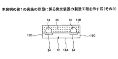
11,41,61 基板
12 発光素子
12A,13A 上面
12B,16B,62B 下面
12C,17A,44B,44C 側面
13,31 蛍光体含有樹脂
13A,64A,64B 面
14 バンプ
16,42,62 基板本体
17,44 凹部
17B,44A 底面
18 貫通孔
19 配線パターン
21 ビア
22 配線
24 電極
35 マスキング材
36 容器
36A 外周面
51 反射部材
63 透光性部材
64 収容部
D1 深さ
H1,H2 高さ
M1 厚さ
W1〜W3 幅
θ1〜θ3 角度
Claims (2)
- 発光素子と、
蛍光体含有樹脂と、
前記発光素子が配設される基板とを備えた発光装置であって、
前記基板は、発光素子を収容する凹部を有しており、
前記蛍光体含有樹脂を、前記基板と接触しないように前記発光素子の少なくとも上面及び側面を覆うように設けると共に、
前記蛍光体含有樹脂と前記凹部の側面及び底面とを離間させ、
前記凹部は、該凹部の底面から前記発光素子の上面までは等しい幅とされており、前記発光素子の上面よりも上方は、前記発光素子の上面から上方に向けて幅広となるような形状であることを特徴とする発光装置。 - 前記幅広の形状とされた前記凹部の側面に、前記発光素子が放出する光を反射する反射部材を設けたことを特徴とする請求項1記載の発光装置。
Priority Applications (1)
| Application Number | Priority Date | Filing Date | Title |
|---|---|---|---|
| JP2006027436A JP5038631B2 (ja) | 2006-02-03 | 2006-02-03 | 発光装置 |
Applications Claiming Priority (1)
| Application Number | Priority Date | Filing Date | Title |
|---|---|---|---|
| JP2006027436A JP5038631B2 (ja) | 2006-02-03 | 2006-02-03 | 発光装置 |
Publications (3)
| Publication Number | Publication Date |
|---|---|
| JP2007208136A JP2007208136A (ja) | 2007-08-16 |
| JP2007208136A5 JP2007208136A5 (ja) | 2009-02-12 |
| JP5038631B2 true JP5038631B2 (ja) | 2012-10-03 |
Family
ID=38487311
Family Applications (1)
| Application Number | Title | Priority Date | Filing Date |
|---|---|---|---|
| JP2006027436A Expired - Fee Related JP5038631B2 (ja) | 2006-02-03 | 2006-02-03 | 発光装置 |
Country Status (1)
| Country | Link |
|---|---|
| JP (1) | JP5038631B2 (ja) |
Families Citing this family (11)
| Publication number | Priority date | Publication date | Assignee | Title |
|---|---|---|---|---|
| KR101468696B1 (ko) * | 2007-12-31 | 2014-12-08 | 서울반도체 주식회사 | 발광 소자 |
| DE102008057174A1 (de) * | 2008-11-13 | 2010-05-20 | Osram Opto Semiconductors Gmbh | Oberflächenmontierbare Vorrichtung |
| KR101573888B1 (ko) * | 2009-03-31 | 2015-12-04 | 서울반도체 주식회사 | 측면 발광 다이오드 패키지 |
| JP2012142410A (ja) | 2010-12-28 | 2012-07-26 | Rohm Co Ltd | 発光素子ユニットおよびその製造方法、発光素子パッケージならびに照明装置 |
| KR101939333B1 (ko) * | 2011-10-07 | 2019-01-16 | 서울바이오시스 주식회사 | 발광 다이오드 패키지 |
| JP6118575B2 (ja) * | 2013-02-12 | 2017-04-19 | 日亜化学工業株式会社 | 発光装置 |
| KR102189129B1 (ko) * | 2014-06-02 | 2020-12-09 | 엘지이노텍 주식회사 | 발광 소자 모듈 |
| JP6755090B2 (ja) | 2014-12-11 | 2020-09-16 | シチズン電子株式会社 | 発光装置及び発光装置の製造方法 |
| JP2017130588A (ja) * | 2016-01-21 | 2017-07-27 | 旭化成株式会社 | 紫外線発光装置 |
| JP6279702B2 (ja) * | 2016-12-26 | 2018-02-14 | ローム株式会社 | 発光素子パッケージおよび照明装置 |
| US20190334066A1 (en) * | 2017-09-12 | 2019-10-31 | Lg Innotek Co., Ltd. | Light emitting device package |
Family Cites Families (6)
| Publication number | Priority date | Publication date | Assignee | Title |
|---|---|---|---|---|
| JP2002141559A (ja) * | 2000-10-31 | 2002-05-17 | Sanken Electric Co Ltd | 発光半導体チップ組立体及び発光半導体リードフレーム |
| JP2002252372A (ja) * | 2001-02-26 | 2002-09-06 | Nichia Chem Ind Ltd | 発光ダイオード |
| JP4072084B2 (ja) * | 2003-03-24 | 2008-04-02 | 京セラ株式会社 | 発光素子収納用パッケージおよび発光装置 |
| EP3166152B1 (en) * | 2003-08-19 | 2020-04-15 | Nichia Corporation | Semiconductor light emitting diode and method of manufacturing its substrate |
| JP2005150484A (ja) * | 2003-11-18 | 2005-06-09 | Nichia Chem Ind Ltd | 半導体発光素子用被膜及びその製造方法並びに半導体発光装置 |
| JP4516337B2 (ja) * | 2004-03-25 | 2010-08-04 | シチズン電子株式会社 | 半導体発光装置 |
-
2006
- 2006-02-03 JP JP2006027436A patent/JP5038631B2/ja not_active Expired - Fee Related
Also Published As
| Publication number | Publication date |
|---|---|
| JP2007208136A (ja) | 2007-08-16 |
Similar Documents
| Publication | Publication Date | Title |
|---|---|---|
| JP5038631B2 (ja) | 発光装置 | |
| JP4828248B2 (ja) | 発光装置及びその製造方法 | |
| US7982237B2 (en) | Light emitting device package including a semiconductor substrate having at least one surface | |
| JP5175488B2 (ja) | 多層反射面構造を有するledパッケージ | |
| US8237187B2 (en) | Package structure for chip and method for forming the same | |
| TWI381555B (zh) | 發光二極體封裝結構與發光元件 | |
| JP4655029B2 (ja) | 発光装置および半導体発光素子の製造方法 | |
| EP1804302B1 (en) | Light emitting semiconductor device and method for manufacturing the same | |
| JP2013153068A (ja) | 配線基板、発光装置及び配線基板の製造方法 | |
| US20130105978A1 (en) | Silicon submount for light emitting diode and method of forming the same | |
| KR20120060469A (ko) | 발광소자 패키지 및 그 제조 방법 | |
| US20120056223A1 (en) | Led package structure and packaging method thereof | |
| US8487339B2 (en) | Light-emitting diode chip package body and method for manufacturing same | |
| US20070235863A1 (en) | LED chip array module | |
| KR102461968B1 (ko) | 발광 소자 | |
| JP2008140873A (ja) | フリップチップ実装されたiii−v族半導体素子およびその製造方法 | |
| JP7112596B2 (ja) | 半導体発光デバイス | |
| JP4383059B2 (ja) | 発光素子収納用パッケージおよび発光装置 | |
| JP2006093626A (ja) | 半導体発光装置 | |
| JP4846505B2 (ja) | 発光装置およびその製造方法 | |
| WO2011037185A1 (ja) | 実装用基板、発光体、および実装用基板の製造方法 | |
| JP4322181B2 (ja) | 半導体装置の製造方法 | |
| JP5912471B2 (ja) | 半導体デバイス | |
| TWI792460B (zh) | 顯示面板及其製造方法 | |
| JP2007201104A (ja) | 発光装置 |
Legal Events
| Date | Code | Title | Description |
|---|---|---|---|
| A521 | Request for written amendment filed |
Free format text: JAPANESE INTERMEDIATE CODE: A523 Effective date: 20081219 |
|
| A621 | Written request for application examination |
Free format text: JAPANESE INTERMEDIATE CODE: A621 Effective date: 20081219 |
|
| A977 | Report on retrieval |
Free format text: JAPANESE INTERMEDIATE CODE: A971007 Effective date: 20110427 |
|
| A131 | Notification of reasons for refusal |
Free format text: JAPANESE INTERMEDIATE CODE: A131 Effective date: 20110510 |
|
| A521 | Request for written amendment filed |
Free format text: JAPANESE INTERMEDIATE CODE: A523 Effective date: 20110701 |
|
| A131 | Notification of reasons for refusal |
Free format text: JAPANESE INTERMEDIATE CODE: A131 Effective date: 20111108 |
|
| A521 | Request for written amendment filed |
Free format text: JAPANESE INTERMEDIATE CODE: A523 Effective date: 20111228 |
|
| TRDD | Decision of grant or rejection written | ||
| A01 | Written decision to grant a patent or to grant a registration (utility model) |
Free format text: JAPANESE INTERMEDIATE CODE: A01 Effective date: 20120703 |
|
| A01 | Written decision to grant a patent or to grant a registration (utility model) |
Free format text: JAPANESE INTERMEDIATE CODE: A01 |
|
| A61 | First payment of annual fees (during grant procedure) |
Free format text: JAPANESE INTERMEDIATE CODE: A61 Effective date: 20120706 |
|
| FPAY | Renewal fee payment (event date is renewal date of database) |
Free format text: PAYMENT UNTIL: 20150713 Year of fee payment: 3 |
|
| R150 | Certificate of patent or registration of utility model |
Ref document number: 5038631 Country of ref document: JP Free format text: JAPANESE INTERMEDIATE CODE: R150 Free format text: JAPANESE INTERMEDIATE CODE: R150 |
|
| LAPS | Cancellation because of no payment of annual fees |