JP5028126B2 - 誘電体基板の製造方法 - Google Patents
誘電体基板の製造方法 Download PDFInfo
- Publication number
- JP5028126B2 JP5028126B2 JP2007092829A JP2007092829A JP5028126B2 JP 5028126 B2 JP5028126 B2 JP 5028126B2 JP 2007092829 A JP2007092829 A JP 2007092829A JP 2007092829 A JP2007092829 A JP 2007092829A JP 5028126 B2 JP5028126 B2 JP 5028126B2
- Authority
- JP
- Japan
- Prior art keywords
- dielectric substrate
- conductive film
- hole
- conductor
- via hole
- Prior art date
- Legal status (The legal status is an assumption and is not a legal conclusion. Google has not performed a legal analysis and makes no representation as to the accuracy of the status listed.)
- Expired - Fee Related
Links
- 239000000758 substrate Substances 0.000 title claims description 62
- 238000004519 manufacturing process Methods 0.000 title claims description 8
- 239000004020 conductor Substances 0.000 claims description 41
- 238000000034 method Methods 0.000 claims description 20
- 238000009713 electroplating Methods 0.000 claims description 8
- 229910000679 solder Inorganic materials 0.000 description 15
- 229910052751 metal Inorganic materials 0.000 description 9
- 239000002184 metal Substances 0.000 description 9
- 238000007747 plating Methods 0.000 description 5
- PCHJSUWPFVWCPO-UHFFFAOYSA-N gold Chemical compound [Au] PCHJSUWPFVWCPO-UHFFFAOYSA-N 0.000 description 4
- 229910052737 gold Inorganic materials 0.000 description 4
- 239000010931 gold Substances 0.000 description 4
- BASFCYQUMIYNBI-UHFFFAOYSA-N platinum Chemical compound [Pt] BASFCYQUMIYNBI-UHFFFAOYSA-N 0.000 description 4
- RYGMFSIKBFXOCR-UHFFFAOYSA-N Copper Chemical compound [Cu] RYGMFSIKBFXOCR-UHFFFAOYSA-N 0.000 description 2
- RTAQQCXQSZGOHL-UHFFFAOYSA-N Titanium Chemical compound [Ti] RTAQQCXQSZGOHL-UHFFFAOYSA-N 0.000 description 2
- 238000005422 blasting Methods 0.000 description 2
- 229910052802 copper Inorganic materials 0.000 description 2
- 239000010949 copper Substances 0.000 description 2
- 238000010586 diagram Methods 0.000 description 2
- 239000011521 glass Substances 0.000 description 2
- 230000008018 melting Effects 0.000 description 2
- 238000002844 melting Methods 0.000 description 2
- 230000000149 penetrating effect Effects 0.000 description 2
- 229910052697 platinum Inorganic materials 0.000 description 2
- 238000007650 screen-printing Methods 0.000 description 2
- 238000004544 sputter deposition Methods 0.000 description 2
- 238000000992 sputter etching Methods 0.000 description 2
- 229910052719 titanium Inorganic materials 0.000 description 2
- 239000010936 titanium Substances 0.000 description 2
- 238000007740 vapor deposition Methods 0.000 description 2
- 239000000853 adhesive Substances 0.000 description 1
- 230000001070 adhesive effect Effects 0.000 description 1
- 230000005684 electric field Effects 0.000 description 1
- 238000007772 electroless plating Methods 0.000 description 1
- SWELZOZIOHGSPA-UHFFFAOYSA-N palladium silver Chemical compound [Pd].[Ag] SWELZOZIOHGSPA-UHFFFAOYSA-N 0.000 description 1
- 230000002093 peripheral effect Effects 0.000 description 1
- 229910052709 silver Inorganic materials 0.000 description 1
- 239000004332 silver Substances 0.000 description 1
- 238000005245 sintering Methods 0.000 description 1
Images
Landscapes
- Printing Elements For Providing Electric Connections Between Printed Circuits (AREA)
Description
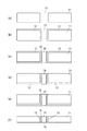
12;スルーホール
13;第1の導電膜
14;導電体
15;第2の導電膜
16;ビアホール
17;ハンダボール
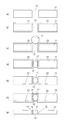
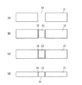
21;誘電体基板
22;スルーホール
23;導電体
24;導電膜
Claims (1)
- ビアホールを有する誘電体基板の製造方法において、
誘電体基板にスルーホールを形成する工程と、
該スルーホールの側壁および前記誘電体基板の表面に該誘電体基板に接着性の良い第1の導電膜を形成する工程と、
該第1の導電膜で側壁が被覆された前記スルーホール内に導電体を充填する工程と、
前記誘電体基板の一方の面上の前記第1の導電膜を除去した後、前記スルーホール内の前記第1の導電膜と前記導電体との隙間に、該第1の導電膜を電極として用いた電界メッキ法により該第1の導電膜と前記導電体のいずれとも接着性の良い第2の導電膜を形成し、前記スルーホール内を前記第1の導電膜、前記導電体及び前記第2の導電膜によって充填された前記ビアホールを形成する工程と、
該ビアホールを形成後、少なくとも前記誘電体基板の他方の面上に残る前記第1の導電膜を除去する工程とを含むことを特徴とする誘電体基板の製造方法。
Priority Applications (1)
| Application Number | Priority Date | Filing Date | Title |
|---|---|---|---|
| JP2007092829A JP5028126B2 (ja) | 2007-03-30 | 2007-03-30 | 誘電体基板の製造方法 |
Applications Claiming Priority (1)
| Application Number | Priority Date | Filing Date | Title |
|---|---|---|---|
| JP2007092829A JP5028126B2 (ja) | 2007-03-30 | 2007-03-30 | 誘電体基板の製造方法 |
Publications (2)
| Publication Number | Publication Date |
|---|---|
| JP2008251935A JP2008251935A (ja) | 2008-10-16 |
| JP5028126B2 true JP5028126B2 (ja) | 2012-09-19 |
Family
ID=39976513
Family Applications (1)
| Application Number | Title | Priority Date | Filing Date |
|---|---|---|---|
| JP2007092829A Expired - Fee Related JP5028126B2 (ja) | 2007-03-30 | 2007-03-30 | 誘電体基板の製造方法 |
Country Status (1)
| Country | Link |
|---|---|
| JP (1) | JP5028126B2 (ja) |
Families Citing this family (2)
| Publication number | Priority date | Publication date | Assignee | Title |
|---|---|---|---|---|
| KR100968977B1 (ko) * | 2008-10-17 | 2010-07-14 | 삼성전기주식회사 | 무수축 세라믹 기판 및 무수축 세라믹 기판의 제조 방법 |
| KR101153492B1 (ko) * | 2010-08-24 | 2012-06-11 | 삼성전기주식회사 | 프로브 카드용 세라믹 기판 제조 방법 및 프로브 카드용 세라믹 기판 |
Family Cites Families (2)
| Publication number | Priority date | Publication date | Assignee | Title |
|---|---|---|---|---|
| JP2001332650A (ja) * | 2000-05-24 | 2001-11-30 | Tateyama Kagaku Kogyo Kk | 電子素子用基板とその製造方法並びに電子素子とその製造方法 |
| JP2007081100A (ja) * | 2005-09-14 | 2007-03-29 | Tdk Corp | 配線基板およびその製造方法 |
-
2007
- 2007-03-30 JP JP2007092829A patent/JP5028126B2/ja not_active Expired - Fee Related
Also Published As
| Publication number | Publication date |
|---|---|
| JP2008251935A (ja) | 2008-10-16 |
Similar Documents
| Publication | Publication Date | Title |
|---|---|---|
| US6815348B2 (en) | Method of plugging through-holes in silicon substrate | |
| US10790209B2 (en) | Wiring circuit substrate, semiconductor device, method of producing the wiring circuit substrate, and method of producing the semiconductor device | |
| EP3220417B1 (en) | Wiring circuit board, semiconductor device, wiring circuit board manufacturing method, and semiconductor device manufacturing method | |
| JP4904242B2 (ja) | 配線基板及びその製造方法 | |
| WO2006082784A1 (ja) | 多層プリント配線板 | |
| WO2006082785A1 (ja) | 多層プリント配線板 | |
| JP4713602B2 (ja) | 基板モジュールおよびその製造方法ならびに電子機器 | |
| JP2017204527A (ja) | 配線回路基板及びその製造方法 | |
| KR20140020114A (ko) | 금속 방열기판 및 그 제조방법 | |
| JP5028126B2 (ja) | 誘電体基板の製造方法 | |
| CN109075125B (zh) | 用于填充陶瓷衬底的通孔的方法以及由此形成的陶瓷衬底通孔填充物 | |
| JP6566811B2 (ja) | 半田チップ、半田チップを用いた端子付きガラス基板の製造方法 | |
| KR101119259B1 (ko) | 하이브리드형 방열기판 및 그 제조방법 | |
| JP2017228727A (ja) | 配線基板及びその製造方法 | |
| WO2006082783A1 (ja) | 多層プリント配線板 | |
| JP4471730B2 (ja) | 両面配線基板及びその製造方法 | |
| KR20110088196A (ko) | 메탈코어 pcb 기판의 예열 장치 및 이를 이용한 메탈코어 pcb 기판의 솔더링 방법 | |
| TW201108903A (en) | Printed wiring board and method for producing the same | |
| JP2006196599A (ja) | 基板両面の導通方法及び配線基板 | |
| JP6936965B2 (ja) | 配線基板及びその製造方法 | |
| JP7182856B2 (ja) | 配線基板及びその製造方法 | |
| JP2005129874A (ja) | 半導体チップ、半導体チップの製造方法、半導体実装基板、電子デバイスおよび電子機器 | |
| JP2003318507A (ja) | 回路基板の製造法 | |
| JP2757594B2 (ja) | フィルムキャリア装置 | |
| JPH08107257A (ja) | 電磁波シールドを有するプリント配線板の製造方法 |
Legal Events
| Date | Code | Title | Description |
|---|---|---|---|
| A621 | Written request for application examination |
Free format text: JAPANESE INTERMEDIATE CODE: A621 Effective date: 20100122 |
|
| A977 | Report on retrieval |
Free format text: JAPANESE INTERMEDIATE CODE: A971007 Effective date: 20110914 |
|
| A131 | Notification of reasons for refusal |
Free format text: JAPANESE INTERMEDIATE CODE: A131 Effective date: 20110927 |
|
| A521 | Request for written amendment filed |
Free format text: JAPANESE INTERMEDIATE CODE: A523 Effective date: 20111121 |
|
| TRDD | Decision of grant or rejection written | ||
| A01 | Written decision to grant a patent or to grant a registration (utility model) |
Free format text: JAPANESE INTERMEDIATE CODE: A01 Effective date: 20120605 |
|
| A01 | Written decision to grant a patent or to grant a registration (utility model) |
Free format text: JAPANESE INTERMEDIATE CODE: A01 |
|
| A61 | First payment of annual fees (during grant procedure) |
Free format text: JAPANESE INTERMEDIATE CODE: A61 Effective date: 20120625 |
|
| FPAY | Renewal fee payment (event date is renewal date of database) |
Free format text: PAYMENT UNTIL: 20150629 Year of fee payment: 3 |
|
| R150 | Certificate of patent or registration of utility model |
Ref document number: 5028126 Country of ref document: JP Free format text: JAPANESE INTERMEDIATE CODE: R150 Free format text: JAPANESE INTERMEDIATE CODE: R150 |
|
| R250 | Receipt of annual fees |
Free format text: JAPANESE INTERMEDIATE CODE: R250 |
|
| R250 | Receipt of annual fees |
Free format text: JAPANESE INTERMEDIATE CODE: R250 |
|
| R250 | Receipt of annual fees |
Free format text: JAPANESE INTERMEDIATE CODE: R250 |
|
| LAPS | Cancellation because of no payment of annual fees |