JP5000293B2 - 不揮発性半導体メモリ装置 - Google Patents
不揮発性半導体メモリ装置 Download PDFInfo
- Publication number
- JP5000293B2 JP5000293B2 JP2006356457A JP2006356457A JP5000293B2 JP 5000293 B2 JP5000293 B2 JP 5000293B2 JP 2006356457 A JP2006356457 A JP 2006356457A JP 2006356457 A JP2006356457 A JP 2006356457A JP 5000293 B2 JP5000293 B2 JP 5000293B2
- Authority
- JP
- Japan
- Prior art keywords
- capacitor
- insulating film
- electrode
- memory device
- active region
- Prior art date
- Legal status (The legal status is an assumption and is not a legal conclusion. Google has not performed a legal analysis and makes no representation as to the accuracy of the status listed.)
- Expired - Fee Related
Links
Images
Classifications
-
- H—ELECTRICITY
- H10—SEMICONDUCTOR DEVICES; ELECTRIC SOLID-STATE DEVICES NOT OTHERWISE PROVIDED FOR
- H10B—ELECTRONIC MEMORY DEVICES
- H10B41/00—Electrically erasable-and-programmable ROM [EEPROM] devices comprising floating gates
- H10B41/10—Electrically erasable-and-programmable ROM [EEPROM] devices comprising floating gates characterised by the top-view layout
-
- H—ELECTRICITY
- H10—SEMICONDUCTOR DEVICES; ELECTRIC SOLID-STATE DEVICES NOT OTHERWISE PROVIDED FOR
- H10B—ELECTRONIC MEMORY DEVICES
- H10B41/00—Electrically erasable-and-programmable ROM [EEPROM] devices comprising floating gates
- H10B41/30—Electrically erasable-and-programmable ROM [EEPROM] devices comprising floating gates characterised by the memory core region
-
- H—ELECTRICITY
- H10—SEMICONDUCTOR DEVICES; ELECTRIC SOLID-STATE DEVICES NOT OTHERWISE PROVIDED FOR
- H10B—ELECTRONIC MEMORY DEVICES
- H10B41/00—Electrically erasable-and-programmable ROM [EEPROM] devices comprising floating gates
- H10B41/60—Electrically erasable-and-programmable ROM [EEPROM] devices comprising floating gates the control gate being a doped region, e.g. single-poly memory cell
-
- H—ELECTRICITY
- H10—SEMICONDUCTOR DEVICES; ELECTRIC SOLID-STATE DEVICES NOT OTHERWISE PROVIDED FOR
- H10B—ELECTRONIC MEMORY DEVICES
- H10B69/00—Erasable-and-programmable ROM [EPROM] devices not provided for in groups H10B41/00 - H10B63/00, e.g. ultraviolet erasable-and-programmable ROM [UVEPROM] devices
-
- H—ELECTRICITY
- H10—SEMICONDUCTOR DEVICES; ELECTRIC SOLID-STATE DEVICES NOT OTHERWISE PROVIDED FOR
- H10D—INORGANIC ELECTRIC SEMICONDUCTOR DEVICES
- H10D30/00—Field-effect transistors [FET]
- H10D30/60—Insulated-gate field-effect transistors [IGFET]
- H10D30/68—Floating-gate IGFETs
- H10D30/681—Floating-gate IGFETs having only two programming levels
- H10D30/683—Floating-gate IGFETs having only two programming levels programmed by tunnelling of carriers, e.g. Fowler-Nordheim tunnelling
-
- H—ELECTRICITY
- H10—SEMICONDUCTOR DEVICES; ELECTRIC SOLID-STATE DEVICES NOT OTHERWISE PROVIDED FOR
- H10D—INORGANIC ELECTRIC SEMICONDUCTOR DEVICES
- H10D30/00—Field-effect transistors [FET]
- H10D30/60—Insulated-gate field-effect transistors [IGFET]
- H10D30/68—Floating-gate IGFETs
- H10D30/6891—Floating-gate IGFETs characterised by the shapes, relative sizes or dispositions of the floating gate electrode
Landscapes
- Semiconductor Memories (AREA)
- Non-Volatile Memory (AREA)
Description
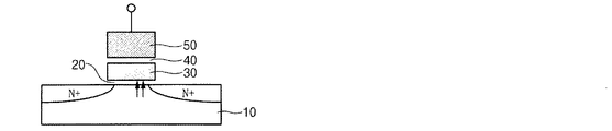
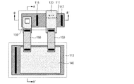
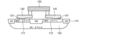
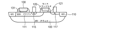
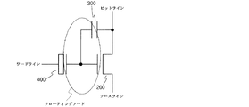
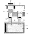
120 トランジスタ電極
130 第1キャパシタ電極
140 第2キャパシタ電極
150、160 金属ライン
170 選択トランジスタ電極
Claims (7)
- 半導体基板と、
前記半導体基板に形成された第1活性領域及び第2活性領域と、
前記第1活性領域及び第2活性領域とを分離する素子分離領域と、
前記第1活性領域に第1絶縁膜を媒介として該第1絶縁膜上に形成されるセンス用トランジスタのゲート電極と、
前記第1活性領域に第2絶縁膜を媒介として該第2絶縁膜上に形成される第1キャパシタのトンネリング電極と、
前記第2活性領域内に第3絶縁膜を媒介として該第3絶縁膜上に形成される第2キャパシタのコントロール電極と、
を備え、
前記第2キャパシタのコントロール電極は、前記素子分離領域とはオーバーラップせずに配置され、寄生キャパシタンスを減らし、
前記センス用トランジスタのゲート電極、前記第1キャパシタのトンネリング電極及び第2キャパシタのコントロール電極は平面上、互いに分離されており、前記第2キャパシタのコントロール電極は金属ラインによって、それぞれ前記センス用トランジスタのゲート電極及び前記第1キャパシタのトンネリング電極に電気的に接続されたことを特徴とする不揮発性半導体メモリ装置。 - 前記第1キャパシタのトンネリング電極は、前記第1活性領域上から前記素子分離領域上まで伸び、
前記第1キャパシタのトンネリング電極と前記第2キャパシタのコントロール電極とを接続する前記金属ラインは、前記素子分離領域上で前記第1キャパシタのトンネリング電極に接続されたことを特徴とする請求項1に記載の不揮発性半導体メモリ装置。 - 前記第1絶縁膜の厚さが、前記第2絶縁膜の厚さより大きいことを特徴とする請求項1に記載の不揮発性半導体メモリ装置。
- 前記第1絶縁膜と前記第3絶縁膜の厚さが、等しいことを特徴とする請求項1に記載の不揮発性半導体メモリ装置。
- 前記第1絶縁膜と前記第3絶縁膜が、同時に形成されることを特徴とする請求項1に記載の不揮発性半導体メモリ装置。
- 前記第1活性領域に第4絶縁膜を媒介として形成された選択トランジスタのゲート電極をさらに備えることを特徴とする請求項1に記載の不揮発性半導体メモリ装置。
- 前記第1キャパシタと前記半導体基板とが共有する前記第1活性領域の接合は、前記センス用トランジスタのドレインを形成し、前記センス用トランジスタのゲート電極を基準に、前記ドレインに対応する前記第1活性領域の接合は、前記センス用トランジスタのソースを形成することを特徴とする請求項1に記載の不揮発性半導体メモリ装置。
Applications Claiming Priority (2)
| Application Number | Priority Date | Filing Date | Title |
|---|---|---|---|
| KR1020050134385A KR100667909B1 (ko) | 2005-12-29 | 2005-12-29 | 비휘발성 반도체 메모리 장치 |
| KR10-2005-0134385 | 2005-12-29 |
Publications (2)
| Publication Number | Publication Date |
|---|---|
| JP2007184612A JP2007184612A (ja) | 2007-07-19 |
| JP5000293B2 true JP5000293B2 (ja) | 2012-08-15 |
Family
ID=37867841
Family Applications (1)
| Application Number | Title | Priority Date | Filing Date |
|---|---|---|---|
| JP2006356457A Expired - Fee Related JP5000293B2 (ja) | 2005-12-29 | 2006-12-28 | 不揮発性半導体メモリ装置 |
Country Status (3)
| Country | Link |
|---|---|
| US (1) | US7772638B2 (ja) |
| JP (1) | JP5000293B2 (ja) |
| KR (1) | KR100667909B1 (ja) |
Families Citing this family (6)
| Publication number | Priority date | Publication date | Assignee | Title |
|---|---|---|---|---|
| KR20100079176A (ko) * | 2008-12-30 | 2010-07-08 | 주식회사 동부하이텍 | 이이피롬 소자 및 그 제조 방법 |
| GB201111916D0 (en) * | 2011-07-12 | 2011-08-24 | Cambridge Silicon Radio Ltd | Single poly non-volatile memory cells |
| EP2639817A1 (en) * | 2012-03-12 | 2013-09-18 | eMemory Technology Inc. | Method of fabricating a single-poly floating-gate memory device |
| KR101586413B1 (ko) * | 2014-12-12 | 2016-01-18 | 주식회사 윙코 | 단일 폴리 비휘발성 메모리 |
| CN107425003B (zh) * | 2016-05-18 | 2020-07-14 | 硅存储技术公司 | 制造分裂栅非易失性闪存单元的方法 |
| WO2017200709A1 (en) * | 2016-05-18 | 2017-11-23 | Silicon Storage Technology, Inc. | Method of making split gate non-volatile flash memory cell |
Family Cites Families (17)
| Publication number | Priority date | Publication date | Assignee | Title |
|---|---|---|---|---|
| JPS6057673A (ja) * | 1983-09-08 | 1985-04-03 | Nec Corp | Mos型半導体装置 |
| US4807003A (en) * | 1986-12-19 | 1989-02-21 | National Semiconductor Corp. | High-reliablity single-poly eeprom cell |
| IT1199828B (it) * | 1986-12-22 | 1989-01-05 | Sgs Microelettronica Spa | Cella di memoria eeprom a singolo livello di polisilicio scrivibile e cancellabile bit a bit |
| US5282161A (en) * | 1990-12-31 | 1994-01-25 | Sgs-Thomson Microelectronics S.R.L. | Eeprom cell having a read interface isolated from the write/erase interface |
| US5440159A (en) * | 1993-09-20 | 1995-08-08 | Atmel Corporation | Single layer polysilicon EEPROM having uniform thickness gate oxide/capacitor dielectric layer |
| JP3001409B2 (ja) * | 1996-02-19 | 2000-01-24 | モトローラ株式会社 | 2層フローティングゲート構造のマルチビット対応セルを有する不揮発性メモリ及びそのプログラム/消去/読出方法 |
| JP4040102B2 (ja) * | 1996-10-28 | 2008-01-30 | マクロニクス インターナショナル カンパニー リミテッド | 冗長エレメントとして単一ポリシリコンフローティングゲートトランジスタを使用するメモリ冗長回路 |
| US5786614A (en) * | 1997-04-08 | 1998-07-28 | Taiwan Semiconductor Manufacturing Co., Ltd. | Separated floating gate for EEPROM application |
| JPH1187664A (ja) * | 1997-04-28 | 1999-03-30 | Nippon Steel Corp | 半導体装置及びその製造方法 |
| US5885871A (en) * | 1997-07-31 | 1999-03-23 | Stmicrolelectronics, Inc. | Method of making EEPROM cell structure |
| JP2000031395A (ja) * | 1998-07-13 | 2000-01-28 | Nec Corp | 半導体装置とその製造方法 |
| EP0977265A1 (en) * | 1998-07-30 | 2000-02-02 | STMicroelectronics S.r.l. | Circuit structure comprising a parasitic transistor having a very high threshold voltage |
| US6324097B1 (en) * | 1999-08-26 | 2001-11-27 | Mosel Vitelic Inc. | Single poly non-volatile memory structure and its fabricating method |
| JP4068519B2 (ja) * | 2002-07-08 | 2008-03-26 | 株式会社東芝 | 有効期限付き機能利用装置 |
| JP2004165182A (ja) * | 2002-11-08 | 2004-06-10 | Ricoh Co Ltd | 半導体装置 |
| KR100493061B1 (ko) * | 2003-06-20 | 2005-06-02 | 삼성전자주식회사 | 비휘발성 메모리가 내장된 단일 칩 데이터 처리 장치 |
| JP2005191057A (ja) * | 2003-12-24 | 2005-07-14 | Seiko Epson Corp | 不揮発性半導体装置及びその製造方法 |
-
2005
- 2005-12-29 KR KR1020050134385A patent/KR100667909B1/ko not_active Expired - Fee Related
-
2006
- 2006-12-28 JP JP2006356457A patent/JP5000293B2/ja not_active Expired - Fee Related
- 2006-12-29 US US11/647,203 patent/US7772638B2/en active Active
Also Published As
| Publication number | Publication date |
|---|---|
| KR100667909B1 (ko) | 2007-01-11 |
| US7772638B2 (en) | 2010-08-10 |
| JP2007184612A (ja) | 2007-07-19 |
| US20070152262A1 (en) | 2007-07-05 |
Similar Documents
| Publication | Publication Date | Title |
|---|---|---|
| US8592942B2 (en) | Non-volatile semiconductor memory device | |
| US6608345B2 (en) | Nonvolatile semiconductor memory device and semiconductor integrated circuit | |
| JP5893662B2 (ja) | 不揮発性メモリセル構造及びこれをプログラミングし読み出す方法 | |
| CN101377955B (zh) | 电可擦除可编程只读存储器单元及其形成和读取方法 | |
| TWI452679B (zh) | 絕緣體上覆半導體上具有埋設於絕緣層下之第二控制閘極的快閃記憶體晶胞 | |
| JP2001244424A (ja) | 半導体集積回路装置および半導体集積回路装置の製造方法 | |
| JP2007294861A (ja) | 単層ポリシリコン不揮発性メモリーセルの動作方法 | |
| JP2009295781A (ja) | 半導体装置及びその製造方法 | |
| CN101488502A (zh) | 非易失性半导体存储装置 | |
| JP2013239597A (ja) | 半導体集積回路 | |
| US7808054B2 (en) | OTP memory cell, OTP memory, and method of manufacturing OTP memory cell | |
| JP2007173821A (ja) | プログラミング速度を改善したeeprom、その製造方法及びその駆動方法 | |
| US10490438B2 (en) | Non-volatile semiconductor memory device and manufacturing method of p-channel MOS transistor | |
| CN100440516C (zh) | 非易失性存储装置 | |
| US20070241387A1 (en) | Nonvolatile semiconductor memory device | |
| JP5289559B2 (ja) | 不揮発性プログラマブルロジックスイッチ | |
| JP5000293B2 (ja) | 不揮発性半導体メモリ装置 | |
| JP2020035877A (ja) | 半導体装置 | |
| JP2012060005A (ja) | 不揮発性プログラマブルロジックスイッチおよび半導体集積回路 | |
| JP4093359B2 (ja) | 電気的に消去可能なプログラマブルロジックデバイス | |
| JP2006344735A (ja) | 半導体装置 | |
| JP4854375B2 (ja) | 半導体記憶装置及びその製造方法、並びに携帯電子機器 | |
| JP6718115B2 (ja) | 強誘電体メモリ装置 | |
| JP2002043446A (ja) | 不揮発性半導体記憶装置 | |
| JP2010129620A (ja) | 不揮発性半導体記憶装置 |
Legal Events
| Date | Code | Title | Description |
|---|---|---|---|
| A977 | Report on retrieval |
Free format text: JAPANESE INTERMEDIATE CODE: A971007 Effective date: 20100714 |
|
| A131 | Notification of reasons for refusal |
Free format text: JAPANESE INTERMEDIATE CODE: A131 Effective date: 20100722 |
|
| A601 | Written request for extension of time |
Free format text: JAPANESE INTERMEDIATE CODE: A601 Effective date: 20101020 |
|
| A602 | Written permission of extension of time |
Free format text: JAPANESE INTERMEDIATE CODE: A602 Effective date: 20101025 |
|
| A521 | Request for written amendment filed |
Free format text: JAPANESE INTERMEDIATE CODE: A523 Effective date: 20101122 |
|
| A131 | Notification of reasons for refusal |
Free format text: JAPANESE INTERMEDIATE CODE: A131 Effective date: 20101216 |
|
| RD02 | Notification of acceptance of power of attorney |
Free format text: JAPANESE INTERMEDIATE CODE: A7422 Effective date: 20110218 |
|
| RD04 | Notification of resignation of power of attorney |
Free format text: JAPANESE INTERMEDIATE CODE: A7424 Effective date: 20110225 |
|
| A601 | Written request for extension of time |
Free format text: JAPANESE INTERMEDIATE CODE: A601 Effective date: 20110316 |
|
| A602 | Written permission of extension of time |
Free format text: JAPANESE INTERMEDIATE CODE: A602 Effective date: 20110322 |
|
| A521 | Request for written amendment filed |
Free format text: JAPANESE INTERMEDIATE CODE: A523 Effective date: 20110418 |
|
| A131 | Notification of reasons for refusal |
Free format text: JAPANESE INTERMEDIATE CODE: A131 Effective date: 20120110 |
|
| A521 | Request for written amendment filed |
Free format text: JAPANESE INTERMEDIATE CODE: A523 Effective date: 20120410 |
|
| TRDD | Decision of grant or rejection written | ||
| A01 | Written decision to grant a patent or to grant a registration (utility model) |
Free format text: JAPANESE INTERMEDIATE CODE: A01 Effective date: 20120508 |
|
| A01 | Written decision to grant a patent or to grant a registration (utility model) |
Free format text: JAPANESE INTERMEDIATE CODE: A01 |
|
| A61 | First payment of annual fees (during grant procedure) |
Free format text: JAPANESE INTERMEDIATE CODE: A61 Effective date: 20120516 |
|
| R150 | Certificate of patent or registration of utility model |
Ref document number: 5000293 Country of ref document: JP Free format text: JAPANESE INTERMEDIATE CODE: R150 Free format text: JAPANESE INTERMEDIATE CODE: R150 |
|
| FPAY | Renewal fee payment (event date is renewal date of database) |
Free format text: PAYMENT UNTIL: 20150525 Year of fee payment: 3 |
|
| R250 | Receipt of annual fees |
Free format text: JAPANESE INTERMEDIATE CODE: R250 |
|
| R250 | Receipt of annual fees |
Free format text: JAPANESE INTERMEDIATE CODE: R250 |
|
| R250 | Receipt of annual fees |
Free format text: JAPANESE INTERMEDIATE CODE: R250 |
|
| R250 | Receipt of annual fees |
Free format text: JAPANESE INTERMEDIATE CODE: R250 |
|
| R250 | Receipt of annual fees |
Free format text: JAPANESE INTERMEDIATE CODE: R250 |
|
| R250 | Receipt of annual fees |
Free format text: JAPANESE INTERMEDIATE CODE: R250 |
|
| S111 | Request for change of ownership or part of ownership |
Free format text: JAPANESE INTERMEDIATE CODE: R313113 |
|
| R350 | Written notification of registration of transfer |
Free format text: JAPANESE INTERMEDIATE CODE: R350 |
|
| R250 | Receipt of annual fees |
Free format text: JAPANESE INTERMEDIATE CODE: R250 |
|
| R250 | Receipt of annual fees |
Free format text: JAPANESE INTERMEDIATE CODE: R250 |
|
| R250 | Receipt of annual fees |
Free format text: JAPANESE INTERMEDIATE CODE: R250 |
|
| S533 | Written request for registration of change of name |
Free format text: JAPANESE INTERMEDIATE CODE: R313533 |
|
| R371 | Transfer withdrawn |
Free format text: JAPANESE INTERMEDIATE CODE: R371 |
|
| S533 | Written request for registration of change of name |
Free format text: JAPANESE INTERMEDIATE CODE: R313533 |
|
| R250 | Receipt of annual fees |
Free format text: JAPANESE INTERMEDIATE CODE: R250 |
|
| R350 | Written notification of registration of transfer |
Free format text: JAPANESE INTERMEDIATE CODE: R350 |
|
| LAPS | Cancellation because of no payment of annual fees |