JP5000293B2 - Nonvolatile semiconductor memory device - Google Patents
Nonvolatile semiconductor memory device Download PDFInfo
- Publication number
- JP5000293B2 JP5000293B2 JP2006356457A JP2006356457A JP5000293B2 JP 5000293 B2 JP5000293 B2 JP 5000293B2 JP 2006356457 A JP2006356457 A JP 2006356457A JP 2006356457 A JP2006356457 A JP 2006356457A JP 5000293 B2 JP5000293 B2 JP 5000293B2
- Authority
- JP
- Japan
- Prior art keywords
- capacitor
- insulating film
- electrode
- memory device
- active region
- Prior art date
- Legal status (The legal status is an assumption and is not a legal conclusion. Google has not performed a legal analysis and makes no representation as to the accuracy of the status listed.)
- Expired - Fee Related
Links
Images
Classifications
-
- H—ELECTRICITY
- H10—SEMICONDUCTOR DEVICES; ELECTRIC SOLID-STATE DEVICES NOT OTHERWISE PROVIDED FOR
- H10B—ELECTRONIC MEMORY DEVICES
- H10B41/00—Electrically erasable-and-programmable ROM [EEPROM] devices comprising floating gates
- H10B41/10—Electrically erasable-and-programmable ROM [EEPROM] devices comprising floating gates characterised by the top-view layout
-
- H—ELECTRICITY
- H10—SEMICONDUCTOR DEVICES; ELECTRIC SOLID-STATE DEVICES NOT OTHERWISE PROVIDED FOR
- H10B—ELECTRONIC MEMORY DEVICES
- H10B41/00—Electrically erasable-and-programmable ROM [EEPROM] devices comprising floating gates
- H10B41/30—Electrically erasable-and-programmable ROM [EEPROM] devices comprising floating gates characterised by the memory core region
-
- H—ELECTRICITY
- H10—SEMICONDUCTOR DEVICES; ELECTRIC SOLID-STATE DEVICES NOT OTHERWISE PROVIDED FOR
- H10B—ELECTRONIC MEMORY DEVICES
- H10B41/00—Electrically erasable-and-programmable ROM [EEPROM] devices comprising floating gates
- H10B41/60—Electrically erasable-and-programmable ROM [EEPROM] devices comprising floating gates the control gate being a doped region, e.g. single-poly memory cell
-
- H—ELECTRICITY
- H10—SEMICONDUCTOR DEVICES; ELECTRIC SOLID-STATE DEVICES NOT OTHERWISE PROVIDED FOR
- H10B—ELECTRONIC MEMORY DEVICES
- H10B69/00—Erasable-and-programmable ROM [EPROM] devices not provided for in groups H10B41/00 - H10B63/00, e.g. ultraviolet erasable-and-programmable ROM [UVEPROM] devices
-
- H—ELECTRICITY
- H10—SEMICONDUCTOR DEVICES; ELECTRIC SOLID-STATE DEVICES NOT OTHERWISE PROVIDED FOR
- H10D—INORGANIC ELECTRIC SEMICONDUCTOR DEVICES
- H10D30/00—Field-effect transistors [FET]
- H10D30/60—Insulated-gate field-effect transistors [IGFET]
- H10D30/68—Floating-gate IGFETs
- H10D30/681—Floating-gate IGFETs having only two programming levels
- H10D30/683—Floating-gate IGFETs having only two programming levels programmed by tunnelling of carriers, e.g. Fowler-Nordheim tunnelling
-
- H—ELECTRICITY
- H10—SEMICONDUCTOR DEVICES; ELECTRIC SOLID-STATE DEVICES NOT OTHERWISE PROVIDED FOR
- H10D—INORGANIC ELECTRIC SEMICONDUCTOR DEVICES
- H10D30/00—Field-effect transistors [FET]
- H10D30/60—Insulated-gate field-effect transistors [IGFET]
- H10D30/68—Floating-gate IGFETs
- H10D30/6891—Floating-gate IGFETs characterised by the shapes, relative sizes or dispositions of the floating gate electrode
Landscapes
- Semiconductor Memories (AREA)
- Non-Volatile Memory (AREA)
Description
本発明は、不揮発性半導体メモリ装置に関し、さらに詳細には、埋め込み半導体装置で書き込みと消去を繰り返し得る不揮発性メモリ機能を提供する不揮発性半導体メモリ装置に関する。 The present invention relates to a nonvolatile semiconductor memory device, and more particularly, to a nonvolatile semiconductor memory device that provides a nonvolatile memory function that allows repeated writing and erasing in an embedded semiconductor device.
デジタル機器の使用の増加に伴い、情報を格納するための記憶装置は必須機能として、特に情報の書き込み/消去を繰り返し得る不揮発性半導体メモリ装置は、その使用が次第に増加しつつある。 As the use of digital devices increases, a storage device for storing information is an indispensable function, and in particular, the use of nonvolatile semiconductor memory devices capable of repeatedly writing / erasing information is gradually increasing.
不揮発性メモリ機能を有する埋め込み(embedded)半導体装置は、メモリ素子とこれを駆動するためのロジック(logic)回路を単一チップで実現したものであり、ロジック半導体製造技術と不揮発性メモリ装置の製造技術を統合して製造される。 An embedded semiconductor device having a nonvolatile memory function is a device in which a memory element and a logic circuit for driving the memory element are realized on a single chip. Logic semiconductor manufacturing technology and manufacture of a nonvolatile memory device Manufactured with integrated technology.
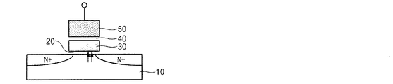
図1は、従来の不揮発性半導体メモリ装置のセル構造を示す断面図である。 FIG. 1 is a cross-sectional view showing a cell structure of a conventional nonvolatile semiconductor memory device.
図1に示すように、従来の不揮発性半導体メモリ装置は、半導体基板10に第1絶縁膜20のトンネリング酸化膜を媒介としてフローティング電極30が形成されており、フローティング電極30上に第2絶縁膜40を媒介としてコントロール電極50を積層した構造で形成されている。
As shown in FIG. 1, in a conventional nonvolatile semiconductor memory device, a floating
このように、二重ゲート構造を有するスタックゲート型のセル構造を適用した従来の不揮発性半導体メモリ装置が、埋め込み半導体装置の不揮発性メモリとして用いられる場合に、不揮発性メモリセルを形成するために、ロジック回路工程にトンネリング酸化膜形成、フローティング電極30の形成、フローティング電極上に第2絶縁膜40を形成しコントロール電極50を形成するなどの追加工程が必須となる。これにより、工程が複雑となり、原価が増加するという問題がある。
As described above, when a conventional nonvolatile semiconductor memory device using a stack gate type cell structure having a double gate structure is used as a nonvolatile memory of an embedded semiconductor device, a nonvolatile memory cell is formed. In addition, additional steps such as formation of a tunneling oxide film, formation of the floating
また、集積度の増加につれて、積層した形態の不揮発性メモリセルを使用する場合、トポロジー(topology)の過度な増加により後続工程で平坦化が難しくなり、工程の難易度が増加するという問題がある。 In addition, when using non-volatile memory cells in a stacked form as the degree of integration increases, there is a problem that planarization becomes difficult in the subsequent process due to an excessive increase in topology and the difficulty of the process increases. .
本発明は、上述の問題点に鑑みてなされたもので、その目的は、積層された電極構造を有さず、かつ、従来のロジック回路製造工程と共に使用することができる不揮発性半導体メモリ装置を提供することにある。 The present invention has been made in view of the above-described problems, and an object of the present invention is to provide a non-volatile semiconductor memory device that does not have a stacked electrode structure and can be used together with a conventional logic circuit manufacturing process. It is to provide.
上記の目的を達成すべく、本発明の実施の形態に係る不揮発性半導体メモリ装置は、半導体基板と、前記半導体基板に形成された第1活性領域及び第2活性領域と、前記第1活性領域及び第2活性領域とを分離する素子分離領域と、前記第1活性領域に第1絶縁膜を媒介として該第1絶縁膜上に形成されるセンス用トランジスタのゲート電極と、前記第1活性領域に第2絶縁膜を媒介として該第2絶縁膜上に形成される第1キャパシタのトンネリング電極と、前記第2活性領域内に第3絶縁膜を媒介として該第3絶縁膜上に形成される第2キャパシタのコントロール電極と、を備え、前記第2キャパシタのコントロール電極は、前記素子分離領域とはオーバーラップせずに配置され、寄生キャパシタンスを減らし、前記センス用トランジスタのゲート電極、前記第1キャパシタのトンネリング電極及び第2キャパシタのコントロール電極は平面上、互いに分離されており、前記第2キャパシタのコントロール電極は金属ラインによって、それぞれ前記センス用トランジスタのゲート電極及び前記第1キャパシタのトンネリング電極に電気的に接続されたことを特徴とする。
In order to achieve the above object, a nonvolatile semiconductor memory device according to an embodiment of the present invention includes a semiconductor substrate, a first active region and a second active region formed in the semiconductor substrate, and the first active region. And an isolation region separating the second active region, a gate electrode of a sensing transistor formed on the first insulating film through the first insulating film as a medium, and the first active region second and first capacitor tunneling electrode that will be formed on the insulating film, the third Ru formed on the insulating film a third insulating film on the second active region as a medium of the second insulating film as mediated It includes a control electrode of the second capacitor, wherein the control electrode of the second capacitor, and the isolation region is disposed without overlap, reducing the parasitic capacitance, the sensing transistors Gate electrode, the first capacitor tunneling electrode and the second capacitor control electrode on a plane, which are separated from each other, by the second capacitor control electrode metal lines, the gate electrodes and the respective said sensing transistors It is electrically connected to the tunneling electrode of the first capacitor.
好ましい実施の形態において、前記第1キャパシタのトンネリング電極は、前記第1活性領域上から前記素子分離領域上まで伸び、前記第1キャパシタのトンネリング電極と前記第2キャパシタのコントロール電極とを接続する前記金属ラインは、前記素子分離領域上で前記第1キャパシタのトンネリング電極に接続されたことを特徴とする。 In a preferred embodiment, the tunneling electrode of the first capacitor extends from the first active region to the element isolation region, and connects the tunneling electrode of the first capacitor and the control electrode of the second capacitor. The metal line is connected to the tunneling electrode of the first capacitor on the element isolation region .
前記第1絶縁膜と前記第3絶縁膜の厚さが、等しく、前記第1絶縁膜と前記第3絶縁膜が、同時に形成されたことを特徴とする。 The first insulating film and the third insulating film are equal in thickness, and the first insulating film and the third insulating film are formed simultaneously.
前記第1活性領域に第4絶縁膜を媒介として形成された選択トランジスタ電極をさらに備えることを特徴とする。 Wherein the pre-Symbol further comprising a selection transistor electrodes formed a fourth insulating film as an intermediary in the first active region.
本発明の不揮発性半導体メモリ装置は、積層された電極構造を有さず、埋め込み半導体装置でロジック回路製造工程と共に同時に製造して、追加の工程なしに製作できるため、製作が容易かつ原価が低減するという効果がある。 The nonvolatile semiconductor memory device of the present invention does not have a stacked electrode structure, and can be manufactured simultaneously with a logic circuit manufacturing process using an embedded semiconductor device and can be manufactured without an additional process. There is an effect of doing.
以下、本発明の好ましい実施の形態を、添付図面に基づき詳細に説明する。 Hereinafter, preferred embodiments of the present invention will be described in detail with reference to the accompanying drawings.
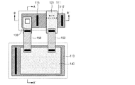
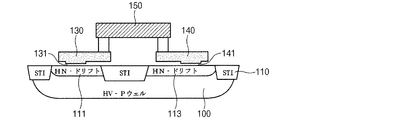
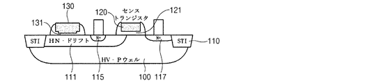
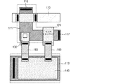
図2は、本発明の一実施の形態に係る不揮発性半導体メモリ装置のセルレイアウト(layout)であり、図3は、図2のA−A´線の断面図であり、図4は、図2のB‐B´線の断面図である。 2 is a cell layout of the nonvolatile semiconductor memory device according to the embodiment of the present invention, FIG. 3 is a cross-sectional view taken along the line AA ′ of FIG. 2, and FIG. 2 is a sectional view taken along line BB ′ in FIG.
図2〜図4に示すように、本発明の不揮発性半導体メモリ装置は、半導体基板100、素子分離領域110、トランジスタ電極120、第1キャパシタ電極130、及び第2キャパシタ電極140を備える。
2 to 4, the nonvolatile semiconductor memory device of the present invention includes a
半導体基板100は、電気的素子が形成される基板であって、例えば、シリコン基板のように、半導体特性を有する材質で形成されて、半導体製造工程により電気的素子が形成される支持台の機能を果たす。
The
素子分離領域110は、半導体基板100に電気的素子が形成される活性領域を電気的に分離する機能を有し、半導体基板100に形成された素子分離領域110により、第1活性領域111と第2活性領域113とが電気的に分離される。また、半導体素子の集積度が増加するにつれて、素子分離領域110は、STI(Shallow Trench Isolation)工程により形成することが好ましい。
The
トランジスタ電極120は、第1活性領域111に形成された第1絶縁膜121を媒介として第1絶縁膜121上に形成されたトランジスタのゲート電極であって、第1活性領域111にトランジスタを形成する。
The
第1キャパシタ電極130は、第1活性領域111に形成された第2絶縁膜131を媒介として第2絶縁膜131上に形成されたキャパシタのゲート電極であって、第1活性領域111に第1キャパシタを形成する。このとき、第1絶縁膜121の厚さは、第2絶縁膜131の厚さより厚いものであって、例えば、第1絶縁膜121は、200〜1000Å程度の範囲を有する酸化膜であり、第2絶縁膜131は、60〜150Å程度の範囲を有する酸化膜である。
The
そして、第1キャパシタ電極130を形成する工程において、厚さの薄い第2絶縁膜131に損傷を与えないように、第1キャパシタ電極130は、第2絶縁膜131の境界で余裕をおいて伸びた境界を有する。
In the step of forming the
そして、第1キャパシタと半導体基板100とが共有する第1活性領域111の接合は、トランジスタのドレイン115を形成し、トランジスタ電極120を基準に、ドレイン115に対応する第1活性領域111の接合は、トランジスタのソース117を形成する。このとき、形成されたトランジスタは、nチャネルトランジスタであって、ドレイン115及びソースも、n型接合を形成することが好ましい。
The junction of the first
第2キャパシタ電極140は、第2活性領域113に形成された第3絶縁膜141を媒介として形成されたキャパシタのゲート電極であって、第2活性領域113に第2キャパシタを形成する。このとき、第2キャパシタ電極140は、トランジスタ電極120及び第1キャパシタ電極130と電気的に接続され、好ましくは、金属ライン150、160により接続される。
The
そして、第2キャパシタ電極140は、第2活性領域113の内部に形成されて、素子分離領域110と重ならないように配置して、寄生キャパシタンスを減少させることが好ましい。第3絶縁膜141は、第1絶縁膜121と同時に形成され、第2キャパシタ電極140もトランジスタ電極120と同時に形成されて、製造工程を簡単にすることが好ましい。したがって、第3絶縁膜141の厚さは、第1絶縁膜121の厚さと等しい酸化膜である。
The
そして、トランジスタ電極120、第1キャパシタ電極130、及び第2キャパシタ電極140は、ポリシリコンで形成することが好ましい。
The
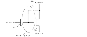
図5は、図2に示す本発明の不揮発性半導体メモリ装置のセルを記号で示す回路図である。 FIG. 5 is a circuit diagram showing the cells of the nonvolatile semiconductor memory device of the present invention shown in FIG. 2 by symbols.
図2〜図5を参照して、本発明の不揮発性半導体メモリ装置の機能及び動作を説明する。本発明の適用例として、図2に示す本発明の不揮発性半導体メモリ装置は、埋め込み半導体素子の不揮発性メモリのセルとして用いられることが好ましい。この場合、埋め込み半導体素子の製造工程に用いられる工程を利用して、追加工程なしに、本発明の不揮発性半導体メモリ装置を実現し得るという長所がある。 The function and operation of the nonvolatile semiconductor memory device of the present invention will be described with reference to FIGS. As an application example of the present invention, the nonvolatile semiconductor memory device of the present invention shown in FIG. 2 is preferably used as a cell of a nonvolatile memory of an embedded semiconductor element. In this case, there is an advantage that the nonvolatile semiconductor memory device of the present invention can be realized by using a process used in the manufacturing process of the embedded semiconductor element without an additional process.
本発明の不揮発性半導体メモリ装置のセルは、総3個の電気的素子を備えるが、トランジスタは、高電圧のNMOSトランジスタであって、ドレイン及びソースを含むセンス(sense)トランジスタ200として機能し、第1キャパシタ電極130と第2絶縁膜131とで形成された第1キャパシタは、電子のトンネリング(tunneling)ウィンドウ(window)として用いられる低電圧ゲート酸化膜を使用した第1MOSキャパシタ(=トンネリングゲート)300である。
The cell of the nonvolatile semiconductor memory device of the present invention includes a total of three electrical elements. The transistor is a high-voltage NMOS transistor that functions as a
そして、第2キャパシタ電極140と第3絶縁膜141で形成された第2キャパシタは、書き込み/消去動作の際、コントロールゲート、すなわちn−接合(junction)に印加された電圧をカップリング(coupling)させるための高電圧ゲート酸化膜を使用した第2MOSキャパシタ(=コントロールゲート)400であり、コントロールゲートは、高電圧素子のソース/ドレインとして用いられるイオン注入を利用したn−接合により接続されて、不揮発性半導体メモリ装置のワードライン(word line)として機能する。
The second capacitor formed of the
コントロールゲートのn−接合は、メモリセルの書き込み/消去時に印加される電圧を第2MOSキャパシタを利用してカップリングさせ、カップリングされた電圧は、接続された金属ライン150、160を介して低電圧ゲート酸化膜の上端の第1キャパシタ電極130に伝達される。このとき、伝達された電圧は、ドレイン端に印加された電圧に応じて、トンネリング酸化膜(=低電圧ゲート酸化膜)の両端にかかり、セルの書き込み/消去動作を行う。
The n - junction of the control gate couples the voltage applied at the time of writing / erasing the memory cell by using the second MOS capacitor, and the coupled voltage is low through the connected
書き込み/消去動作時には、ソース117側をフローティングして、センストランジスタ200を介した電流通路は遮断される。以後、読み出し動作時には、書き込み/消去動作により、F−Nトンネリング現象により互いに接続したトランジスタ電極、第1キャパシタ電極及び第2キャパシタ電極であるポリシリコン内に電子が充填されるか、または放出された状態となる。
During the write / erase operation, the
ポリシリコンに充填または放出された電子は、センストランジスタ200のゲートの下のチャネルのポテンシャル差を表し、センストランジスタ200のチャネルを反転(inversion)させる電圧が変化されることにより、書き込み状態と消去状態の2種類の状態を持つようになる。
Electrons filled or emitted in the polysilicon represent a potential difference between channels under the gate of the
例えば、セルの消去動作の場合、n−接合に接続したワードラインメタルに10〜15Vの高電圧を印加すると、n−接合に接続したコントロールゲートの下端n−接合は、MOSキャパシタカップリングがおき、カップリングされた電圧は、カップリング比(coupling ratio)により、適正電圧が金属ラインに接続されて、トンネリングゲートである第1キャパシタ電極に伝達される。 For example, if the erase operation of the cell, n - is applied a high voltage of 10~15V word line metal connected to the junction, n - lower n of control gate connected to a junction - junction, MOS capacitor coupling place The coupled voltage is transmitted to the first capacitor electrode, which is a tunneling gate, by connecting a proper voltage to the metal line according to a coupling ratio.
カップリング比が約70%の場合、7.0〜10.5Vがトンネリング酸化膜の第2絶縁膜131の上端に伝達されるが、このとき、ドレイン115に接続したビットラインにグラウンド電圧(Vss)が外部から伝達され、酸化膜の厚さが約100Å存在する場合、約7.0〜10.5MeVの電圧がかかる。
When the coupling ratio is about 70%, 7.0 to 10.5 V is transmitted to the upper end of the second
トンネリング酸化膜の両端に垂直方向に電界が印加され、F−Nトンネリング現象により、n−接合側にあった電子は、カップリングされた正(positive)電圧に引かれて、ポリシリコンにトンネリングされる。以後、センストランジスタ200を介してセルのしきい(threshold)電圧を測定する場合、ポリシリコンにトンネリングされた電子により、ポリシリコンゲートの下にチャネルを反転させるための電圧がさらに大きくなるため、しきい電圧は高まる。
An electric field is applied in the vertical direction to both ends of the tunneling oxide film. Due to the FN tunneling phenomenon, electrons on the n - junction side are attracted to the positive voltage coupled and tunneled to the polysilicon. The Thereafter, when the threshold voltage of the cell is measured through the
一般的なSTI工程を使用したフィールド(filed)の場合、ポリシリコンを利用してフィールドを経るとき、寄生フィールドトランジスタが形成され、このトランジスタの降伏(breakdown)電圧としきい電圧は約12〜18V程度で、一般的な用途で使用するため、問題がないが、約20V内外の高い電圧が印加される場合、漏れ電流、カップリング比の減少、降伏電圧の減少(降下)、フィールド反転などの問題が発生する余地がある。 In the case of a field using a general STI process, a parasitic field transistor is formed when passing through the field using polysilicon, and a breakdown voltage and a threshold voltage of the transistor are about 12 to 18V. However, since it is used for general purposes, there is no problem. However, when a high voltage of about 20 V is applied, problems such as leakage current, reduction in coupling ratio, decrease in breakdown voltage (drop), field inversion, etc. There is room to occur.
したがって、本発明でフローティングされたポリシリコン間の接続は、寄生フィールドトランジスタ特性を向上させるために、トンネリング酸化膜のポリシリコン及びセンストランジスタ200のポリシリコンをフローティングゲートのポリシリコンと金属で接続して、ポリシリコン対比書き込み/消去動作時発生し得る降伏電圧の減少及びフィールド反転という問題を解決する。
Therefore, the connection between the floating polysilicons in the present invention is made by connecting the polysilicon of the tunneling oxide film and the polysilicon of the
また、メモリセルの接合は、高電圧による接合の降伏を防止するために、n+接合の場合、ポリシリコンと一定距離を隔てた構造を使用し、ソースの場合、接地レベルの電圧のみを印加するため、従来の低電圧接合と同じ構造を有する。 In addition, in order to prevent the breakdown of the junction due to a high voltage, the junction of the memory cell uses a structure separated from the polysilicon in the case of the n + junction, and in the case of the source, only the ground level voltage is applied. Therefore, it has the same structure as a conventional low voltage junction.
n+ドレイン接合の下には、電界を緩和させるためのn−接合である高電圧用n−イオン注入及びドライブイン(drive−in)熱(thermal)工程を利用したn−接合がある。これらの全ての構造は、従来の高電圧素子に使用していた工程をそのまま利用する。 Under the n + drain junction, n to mitigate the electric field - is joined - n utilizing ion implantation and drive-in (drive-in) heat (thermal) process - the high-voltage n are joined. All these structures utilize the process used for conventional high voltage devices as they are.
コントロールゲートに用いられる第2キャパシタの場合、一般には、フィールド酸化膜側にポリシリコンが伸びるが、本発明では、フィールド酸化膜でポリシリコンとの間で発生される寄生キャパシタンスを減らすために、活性領域内側でポリエッチングされるようにし、トンネリング酸化膜の上端に存在する第1キャパシタ電極は、第2絶縁膜である薄い酸化膜に工程進行時に発生し得るプラズマによる損傷を減らすために、フィールド領域に伸びて金属ラインと接続させる。 In the case of the second capacitor used for the control gate, generally, the polysilicon extends to the field oxide film side. However, in the present invention, in order to reduce the parasitic capacitance generated between the polysilicon and the field oxide film, The first capacitor electrode existing at the upper end of the tunneling oxide film is made to be poly-etched on the inner side of the region, so that the thin oxide film as the second insulating film is reduced in the field region in order to reduce damage caused by plasma that may occur during the process. Connect to the metal line.
埋め込み半導体装置に本発明の不揮発性半導体メモリ装置が用いられる場合、第1絶縁膜及び第3絶縁膜は、高電圧トランジスタの絶縁膜と同じ工程で形成し、第2絶縁膜は、低電圧トランジスタの絶縁膜と同じ工程で形成されるために、別途の工程を追加せず、本発明の不揮発性半導体メモリ装置を有する埋め込み半導体装置の実現が可能である。 When the nonvolatile semiconductor memory device of the present invention is used for the embedded semiconductor device, the first insulating film and the third insulating film are formed in the same process as the insulating film of the high voltage transistor, and the second insulating film is the low voltage transistor. Therefore, an embedded semiconductor device having the nonvolatile semiconductor memory device of the present invention can be realized without adding a separate step.
また、書き込み/消去動作の際、電子のトンネリングを行うトンネリング酸化膜の形成は、従来の埋め込み高電圧工程で高電圧と低電圧用二重ゲートを形成するマスク工程をそのまま使用する。すなわち、ウエハ全面に高電圧用厚いゲート酸化膜(200〜1000Å)を熱酸化工程の方法で成長させ、以後、マスクを利用した選択的ウェットエッチングを適用して、低電圧領域(低電圧N/PMOS素子)をウエハ表面が露出するように選択的エッチングさせる。このとき、トンネリング酸化膜のトンネリングウィンドウ領域も同時にエッチングされる。 In the write / erase operation, a tunneling oxide film for tunneling electrons is formed using a mask process for forming a high voltage and a low voltage double gate in a conventional buried high voltage process. That is, a high-voltage thick gate oxide film (200 to 1000 mm) is grown on the entire surface of the wafer by a thermal oxidation method, and then selective wet etching using a mask is applied to apply a low-voltage region (low-voltage N / The PMOS device is selectively etched so that the wafer surface is exposed. At this time, the tunneling window region of the tunneling oxide film is also etched at the same time.
以後、薄いゲート酸化膜を熱酸化工程方法で酸化させる。したがって、トンネリングウィンドウ領域及び低電圧素子部分には、例えば60〜150Åゲート酸化膜が形成され、残りの高電圧素子領域は、既存の厚いゲート酸化膜に薄いゲート酸化工程時にさらに成長される酸化膜が追加される。 Thereafter, the thin gate oxide film is oxidized by a thermal oxidation process method. Therefore, for example, a 60-150Å gate oxide film is formed in the tunneling window region and the low voltage element portion, and the remaining high voltage element region is further grown on the existing thick gate oxide film during the thin gate oxidation process. Is added.
前記工程により成長されるトンネリング酸化膜は、低電圧酸化膜と等しい厚さを有し、マスクを使用した選択的エッチングの際のトンネリングウィンドウの大きさは、カップリング比を考慮して、横/縦の大きさが、例えば0.4〜1.2μm程度になるようにする。 The tunneling oxide film grown by the above process has a thickness equal to that of the low voltage oxide film, and the size of the tunneling window in the selective etching using the mask is determined by considering the coupling ratio. The vertical size is set to about 0.4 to 1.2 μm, for example.
以上で説明した工程を参照すると、本発明の不揮発性半導体メモリ装置は、従来の埋め込み半導体装置でロジック回路を製作するのに必要な工程を行うと共に製造されるという長所があるため、不揮発性半導体メモリ装置を製作するための追加工程を必要としない。 Referring to the processes described above, the nonvolatile semiconductor memory device of the present invention has an advantage that it performs the processes necessary for manufacturing a logic circuit with a conventional embedded semiconductor device, and is thus manufactured. There is no need for an additional process for manufacturing the memory device.
また、図3及び図4の断面図に示すように、単一層の電極を使用するため、トポロジーが増加しないから、後続の平坦化工程や金属配線工程が容易になる。 Further, as shown in the cross-sectional views of FIGS. 3 and 4, since a single layer electrode is used, the topology does not increase, and the subsequent planarization process and metal wiring process are facilitated.
図5を参照して、本発明の不揮発性半導体メモリ装置の単位セルに対する書き込み/消去/読み出し動作について説明する。 With reference to FIG. 5, a write / erase / read operation for a unit cell of the nonvolatile semiconductor memory device of the present invention will be described.
まず、消去動作特性は、ワードラインを介して約12〜18VのVpp(高電圧)を印加し、印加されたVppは、第2キャパシタであるコントロールキャパシタ400にカップリングされて、第1キャパシタであるトンネリングキャパシタ300の上部に伝達される。このとき、センストランジスタ200のソースノードは、フローティングであるため、トランジスタへの電流通路は形成されない。ドレインノードには、接地電圧、すなわち、0Vが印加されるため、トンネリングキャパシタ300の両端には、垂直方向の電界が発生する。この電界によって、ドレイン端の電子がF−Nトンネリングが発生し、フローティングノードに電子(charge)が格納される。
First, the erase operation characteristic is that Vpp (high voltage) of about 12 to 18V is applied through the word line, and the applied Vpp is coupled to the control capacitor 400 which is the second capacitor, and is applied to the first capacitor. It is transmitted to the upper part of a
すなわち、フローティングノードに電子が注入される場合、注入された電子により、センストランジスタ200のしきい電圧は高まるため、チャネルを逆転させ難くなり、したがって、読み出し電圧を印加してもソース/ドレイン間セル電流は流れない。
That is, when electrons are injected into the floating node, the threshold voltage of the
書き込み動作の場合、ワードラインを介して接地電圧である0Vが印加され、印加されたVssは、コントロールキャパシタ400にカップリングされて、トンネリングキャパシタ300の上部に伝達される。また、センストランジスタ200のソースノードは、フローティングされるため、トランジスタの電流通路は形成されない。また、ドレインノードには、12〜18Vの高電圧を印加し、印加され電圧は、トンネリングキャパシタ300の下端にカップリングされて、トンネリングキャパシタ300の両端には、ワードライン電圧及びドレイン電圧により垂直方向の電界が発生する。この電界により、ポリシリコンに存在する電子がドレイン電圧に引かれて、ビットライン側に放出される。
In the case of a write operation, 0 V, which is a ground voltage, is applied through the word line, and the applied Vss is coupled to the control capacitor 400 and transmitted to the upper portion of the
そして、これにより、しきい電圧が低くなって、読み出し電圧を印加する場合、フローティングゲートの電位がチャネルを十分に反転させ、ソース/ドレイン間電位差により、セル電流が流れるようになる。 Thus, the threshold voltage is lowered, and when a read voltage is applied, the potential of the floating gate sufficiently inverts the channel, and the cell current flows due to the potential difference between the source and drain.
読み出し動作の場合には、一般的なMOSトランジスタの動作と同様に、ビットラインに1.8〜5.0VのVdd電圧を印加し、n−接合からなるワードラインにも、同じ電圧を印加して、ソース/ドレイン間のセル電流を感知する。 In the read operation, the Vdd voltage of 1.8 to 5.0 V is applied to the bit line, and the same voltage is applied to the word line formed of the n - junction as in the operation of a general MOS transistor. The cell current between the source and drain is sensed.
図6は、本発明の他の実施の形態に係る不揮発性半導体メモリ装置のセルレイアウトである。図6は、図2と実質的に同じ構成と機能を有した構成要素に対しては、同じ参照符号を使用する。 FIG. 6 is a cell layout of a nonvolatile semiconductor memory device according to another embodiment of the present invention. FIG. 6 uses the same reference numerals for components having substantially the same configuration and function as FIG.
図6に示すように、本発明の他の実施の形態に係る不揮発性半導体メモリ装置は、一実施の形態の不揮発性半導体メモリ装置で第1活性領域111を伸びて第4絶縁膜を媒介としてポリシリコンで形成された選択トランジスタ電極170をさらに形成した構造を有している。
As shown in FIG. 6, a non-volatile semiconductor memory device according to another embodiment of the present invention is a non-volatile semiconductor memory device according to an embodiment, which extends a first
このとき、第4絶縁膜を第1絶縁膜と同時に形成して、工程の追加なしに選択トランジスタ電極170を形成することが好ましい。そして、ソース117に対応する追加された選択トランジスタ電極170の第1活性領域111の接合は、ドレイン115を形成する。選択トランジスタ電極170により選択トランジスタが形成される。
At this time, it is preferable that the fourth insulating film is formed at the same time as the first insulating film, and the
選択トランジスタは、選択トランジスタ電極170に印加された電圧により、ドレイン115に印加される電圧が、選択的にトンネリングキャパシタに印加されるように調節する。
The selection transistor adjusts so that the voltage applied to the
このとき、選択トランジスタは、ビットラインを介して印加されるドレイン電圧を選択するスイッチ機能を有するトランジスタであって、特定のバイト選択の機能を有する不揮発性半導体メモリ装置を提供する。他の機能や動作は、上述の本発明の一実施の形態と同じである。 At this time, the selection transistor is a transistor having a switching function of selecting a drain voltage applied via the bit line, and provides a nonvolatile semiconductor memory device having a specific byte selection function. Other functions and operations are the same as those in the embodiment of the present invention described above.
上述した本発明の好ましい実施の形態は、例示の目的のために開示されたものであり、本発明の属する技術の分野における通常の知識を有する者であれば、本発明の技術的思想を逸脱しない範囲内で、様々な置換、変形、及び変更が可能であり、このような置換、変更などは、特許請求の範囲に属するものである。 The above-described preferred embodiments of the present invention have been disclosed for the purpose of illustration, and those having ordinary knowledge in the technical field to which the present invention pertains depart from the technical idea of the present invention. Various substitutions, modifications, and alterations are possible within the scope of not being included, and such substitutions, alterations, and the like belong to the scope of the claims.
10、100 半導体基板
120 トランジスタ電極
130 第1キャパシタ電極
140 第2キャパシタ電極
150、160 金属ライン
170 選択トランジスタ電極
10, 100
Claims (7)
前記半導体基板に形成された第1活性領域及び第2活性領域と、
前記第1活性領域及び第2活性領域とを分離する素子分離領域と、
前記第1活性領域に第1絶縁膜を媒介として該第1絶縁膜上に形成されるセンス用トランジスタのゲート電極と、
前記第1活性領域に第2絶縁膜を媒介として該第2絶縁膜上に形成される第1キャパシタのトンネリング電極と、
前記第2活性領域内に第3絶縁膜を媒介として該第3絶縁膜上に形成される第2キャパシタのコントロール電極と、
を備え、
前記第2キャパシタのコントロール電極は、前記素子分離領域とはオーバーラップせずに配置され、寄生キャパシタンスを減らし、
前記センス用トランジスタのゲート電極、前記第1キャパシタのトンネリング電極及び第2キャパシタのコントロール電極は平面上、互いに分離されており、前記第2キャパシタのコントロール電極は金属ラインによって、それぞれ前記センス用トランジスタのゲート電極及び前記第1キャパシタのトンネリング電極に電気的に接続されたことを特徴とする不揮発性半導体メモリ装置。 A semiconductor substrate;
A first active region and a second active region formed in the semiconductor substrate;
An element isolation region that separates the first active region and the second active region;
A gate electrode of a sense transistor formed on the first active region with the first insulating film interposed therebetween;
And tunneling electrodes of the first capacitor second Ru formed on the insulating film a second insulating film as an intermediary in the first active region,
And control electrode of the second capacitor third Ru is formed on the insulating film in the second active region of the third insulating film as a medium,
With
The control electrode of the second capacitor is disposed without overlapping the element isolation region to reduce parasitic capacitance,
The gate electrode of the sense transistor, the first capacitor tunneling electrode and the second capacitor control electrode on a plane, which are separated from each other, by the second capacitor control electrode metal lines, each of the sensing transistors A non-volatile semiconductor memory device, wherein the non-volatile semiconductor memory device is electrically connected to a gate electrode of the first capacitor and a tunneling electrode of the first capacitor.
前記第1キャパシタのトンネリング電極と前記第2キャパシタのコントロール電極とを接続する前記金属ラインは、前記素子分離領域上で前記第1キャパシタのトンネリング電極に接続されたことを特徴とする請求項1に記載の不揮発性半導体メモリ装置。 A tunneling electrode of the first capacitor extends from the first active region to the element isolation region;
The metal line connecting the tunneling electrode of the first capacitor and the control electrode of the second capacitor is connected to the tunneling electrode of the first capacitor on the element isolation region. The nonvolatile semiconductor memory device described.
The junction of the first active region shared by the first capacitor and the semiconductor substrate forms the drain of the sense transistor, and the first electrode corresponding to the drain is based on the gate electrode of the sense transistor. The nonvolatile semiconductor memory device according to claim 1, wherein the junction of the active region forms a source of the sense transistor .
Applications Claiming Priority (2)
| Application Number | Priority Date | Filing Date | Title |
|---|---|---|---|
| KR1020050134385A KR100667909B1 (en) | 2005-12-29 | 2005-12-29 | Nonvolatile Semiconductor Memory Device |
| KR10-2005-0134385 | 2005-12-29 |
Publications (2)
| Publication Number | Publication Date |
|---|---|
| JP2007184612A JP2007184612A (en) | 2007-07-19 |
| JP5000293B2 true JP5000293B2 (en) | 2012-08-15 |
Family
ID=37867841
Family Applications (1)
| Application Number | Title | Priority Date | Filing Date |
|---|---|---|---|
| JP2006356457A Expired - Fee Related JP5000293B2 (en) | 2005-12-29 | 2006-12-28 | Nonvolatile semiconductor memory device |
Country Status (3)
| Country | Link |
|---|---|
| US (1) | US7772638B2 (en) |
| JP (1) | JP5000293B2 (en) |
| KR (1) | KR100667909B1 (en) |
Families Citing this family (6)
| Publication number | Priority date | Publication date | Assignee | Title |
|---|---|---|---|---|
| KR20100079176A (en) * | 2008-12-30 | 2010-07-08 | 주식회사 동부하이텍 | Eeprom device and its fabrication method |
| GB201111916D0 (en) * | 2011-07-12 | 2011-08-24 | Cambridge Silicon Radio Ltd | Single poly non-volatile memory cells |
| EP2639817A1 (en) * | 2012-03-12 | 2013-09-18 | eMemory Technology Inc. | Method of fabricating a single-poly floating-gate memory device |
| KR101586413B1 (en) * | 2014-12-12 | 2016-01-18 | 주식회사 윙코 | Single poly non-volatile memory |
| CN107425003B (en) * | 2016-05-18 | 2020-07-14 | 硅存储技术公司 | Method of manufacturing split gate non-volatile flash memory cell |
| WO2017200709A1 (en) * | 2016-05-18 | 2017-11-23 | Silicon Storage Technology, Inc. | Method of making split gate non-volatile flash memory cell |
Family Cites Families (17)
| Publication number | Priority date | Publication date | Assignee | Title |
|---|---|---|---|---|
| JPS6057673A (en) * | 1983-09-08 | 1985-04-03 | Nec Corp | MOS type semiconductor device |
| US4807003A (en) * | 1986-12-19 | 1989-02-21 | National Semiconductor Corp. | High-reliablity single-poly eeprom cell |
| IT1199828B (en) * | 1986-12-22 | 1989-01-05 | Sgs Microelettronica Spa | SINGLE LEVEL EEPROM MEMORY CELL WRITABLE AND CANCELLABLE POLYSILIC BIT A BIT |
| US5282161A (en) * | 1990-12-31 | 1994-01-25 | Sgs-Thomson Microelectronics S.R.L. | Eeprom cell having a read interface isolated from the write/erase interface |
| US5440159A (en) * | 1993-09-20 | 1995-08-08 | Atmel Corporation | Single layer polysilicon EEPROM having uniform thickness gate oxide/capacitor dielectric layer |
| JP3001409B2 (en) * | 1996-02-19 | 2000-01-24 | モトローラ株式会社 | Non-volatile memory having multi-bit-adaptive cell having two-layer floating gate structure and method for programming / erasing / reading the same |
| JP4040102B2 (en) * | 1996-10-28 | 2008-01-30 | マクロニクス インターナショナル カンパニー リミテッド | Memory redundancy circuit using a single polysilicon floating gate transistor as a redundancy element |
| US5786614A (en) * | 1997-04-08 | 1998-07-28 | Taiwan Semiconductor Manufacturing Co., Ltd. | Separated floating gate for EEPROM application |
| JPH1187664A (en) * | 1997-04-28 | 1999-03-30 | Nippon Steel Corp | Semiconductor device and manufacturing method thereof |
| US5885871A (en) * | 1997-07-31 | 1999-03-23 | Stmicrolelectronics, Inc. | Method of making EEPROM cell structure |
| JP2000031395A (en) * | 1998-07-13 | 2000-01-28 | Nec Corp | Semiconductor device and manufacture thereof |
| EP0977265A1 (en) * | 1998-07-30 | 2000-02-02 | STMicroelectronics S.r.l. | Circuit structure comprising a parasitic transistor having a very high threshold voltage |
| US6324097B1 (en) * | 1999-08-26 | 2001-11-27 | Mosel Vitelic Inc. | Single poly non-volatile memory structure and its fabricating method |
| JP4068519B2 (en) * | 2002-07-08 | 2008-03-26 | 株式会社東芝 | Function using device with expiration date |
| JP2004165182A (en) * | 2002-11-08 | 2004-06-10 | Ricoh Co Ltd | Semiconductor device |
| KR100493061B1 (en) * | 2003-06-20 | 2005-06-02 | 삼성전자주식회사 | Single chip data processing device having embeded nonvolatile memory |
| JP2005191057A (en) * | 2003-12-24 | 2005-07-14 | Seiko Epson Corp | Nonvolatile semiconductor device and manufacturing method thereof |
-
2005
- 2005-12-29 KR KR1020050134385A patent/KR100667909B1/en not_active Expired - Fee Related
-
2006
- 2006-12-28 JP JP2006356457A patent/JP5000293B2/en not_active Expired - Fee Related
- 2006-12-29 US US11/647,203 patent/US7772638B2/en active Active
Also Published As
| Publication number | Publication date |
|---|---|
| KR100667909B1 (en) | 2007-01-11 |
| US7772638B2 (en) | 2010-08-10 |
| JP2007184612A (en) | 2007-07-19 |
| US20070152262A1 (en) | 2007-07-05 |
Similar Documents
| Publication | Publication Date | Title |
|---|---|---|
| US8592942B2 (en) | Non-volatile semiconductor memory device | |
| US6608345B2 (en) | Nonvolatile semiconductor memory device and semiconductor integrated circuit | |
| JP5893662B2 (en) | Nonvolatile memory cell structure and method for programming and reading the same | |
| CN101377955B (en) | Electrically erasable programmable read-only memory (EEPROM) cell and methods for forming and reading the same | |
| TWI452679B (en) | a flash memory cell having a second control gate buried under the insulating layer on the semiconductor overlying insulator | |
| JP2001244424A (en) | Semiconductor integrated circuit device and method of manufacturing semiconductor integrated circuit device | |
| JP2007294861A (en) | Method of operating a single layer polysilicon non-volatile memory cell | |
| JP2009295781A (en) | Semiconductor device and method of manufacturing the same | |
| CN101488502A (en) | non-volatile semiconductor storage device | |
| JP2013239597A (en) | Semiconductor integrated circuit | |
| US7808054B2 (en) | OTP memory cell, OTP memory, and method of manufacturing OTP memory cell | |
| JP2007173821A (en) | EEPROM with improved programming speed, manufacturing method thereof and driving method thereof | |
| US10490438B2 (en) | Non-volatile semiconductor memory device and manufacturing method of p-channel MOS transistor | |
| CN100440516C (en) | non-volatile storage device | |
| US20070241387A1 (en) | Nonvolatile semiconductor memory device | |
| JP5289559B2 (en) | Nonvolatile programmable logic switch | |
| JP5000293B2 (en) | Nonvolatile semiconductor memory device | |
| JP2020035877A (en) | Semiconductor device | |
| JP2012060005A (en) | Non-volatile programmable logic switch and semiconductor integrated circuit | |
| JP4093359B2 (en) | Electrically erasable programmable logic device | |
| JP2006344735A (en) | Semiconductor device | |
| JP4854375B2 (en) | Semiconductor memory device, manufacturing method thereof, and portable electronic device | |
| JP6718115B2 (en) | Ferroelectric memory device | |
| JP2002043446A (en) | Nonvolatile semiconductor memory device | |
| JP2010129620A (en) | Non-volatile semiconductor memory device |
Legal Events
| Date | Code | Title | Description |
|---|---|---|---|
| A977 | Report on retrieval |
Free format text: JAPANESE INTERMEDIATE CODE: A971007 Effective date: 20100714 |
|
| A131 | Notification of reasons for refusal |
Free format text: JAPANESE INTERMEDIATE CODE: A131 Effective date: 20100722 |
|
| A601 | Written request for extension of time |
Free format text: JAPANESE INTERMEDIATE CODE: A601 Effective date: 20101020 |
|
| A602 | Written permission of extension of time |
Free format text: JAPANESE INTERMEDIATE CODE: A602 Effective date: 20101025 |
|
| A521 | Request for written amendment filed |
Free format text: JAPANESE INTERMEDIATE CODE: A523 Effective date: 20101122 |
|
| A131 | Notification of reasons for refusal |
Free format text: JAPANESE INTERMEDIATE CODE: A131 Effective date: 20101216 |
|
| RD02 | Notification of acceptance of power of attorney |
Free format text: JAPANESE INTERMEDIATE CODE: A7422 Effective date: 20110218 |
|
| RD04 | Notification of resignation of power of attorney |
Free format text: JAPANESE INTERMEDIATE CODE: A7424 Effective date: 20110225 |
|
| A601 | Written request for extension of time |
Free format text: JAPANESE INTERMEDIATE CODE: A601 Effective date: 20110316 |
|
| A602 | Written permission of extension of time |
Free format text: JAPANESE INTERMEDIATE CODE: A602 Effective date: 20110322 |
|
| A521 | Request for written amendment filed |
Free format text: JAPANESE INTERMEDIATE CODE: A523 Effective date: 20110418 |
|
| A131 | Notification of reasons for refusal |
Free format text: JAPANESE INTERMEDIATE CODE: A131 Effective date: 20120110 |
|
| A521 | Request for written amendment filed |
Free format text: JAPANESE INTERMEDIATE CODE: A523 Effective date: 20120410 |
|
| TRDD | Decision of grant or rejection written | ||
| A01 | Written decision to grant a patent or to grant a registration (utility model) |
Free format text: JAPANESE INTERMEDIATE CODE: A01 Effective date: 20120508 |
|
| A01 | Written decision to grant a patent or to grant a registration (utility model) |
Free format text: JAPANESE INTERMEDIATE CODE: A01 |
|
| A61 | First payment of annual fees (during grant procedure) |
Free format text: JAPANESE INTERMEDIATE CODE: A61 Effective date: 20120516 |
|
| R150 | Certificate of patent or registration of utility model |
Ref document number: 5000293 Country of ref document: JP Free format text: JAPANESE INTERMEDIATE CODE: R150 Free format text: JAPANESE INTERMEDIATE CODE: R150 |
|
| FPAY | Renewal fee payment (event date is renewal date of database) |
Free format text: PAYMENT UNTIL: 20150525 Year of fee payment: 3 |
|
| R250 | Receipt of annual fees |
Free format text: JAPANESE INTERMEDIATE CODE: R250 |
|
| R250 | Receipt of annual fees |
Free format text: JAPANESE INTERMEDIATE CODE: R250 |
|
| R250 | Receipt of annual fees |
Free format text: JAPANESE INTERMEDIATE CODE: R250 |
|
| R250 | Receipt of annual fees |
Free format text: JAPANESE INTERMEDIATE CODE: R250 |
|
| R250 | Receipt of annual fees |
Free format text: JAPANESE INTERMEDIATE CODE: R250 |
|
| R250 | Receipt of annual fees |
Free format text: JAPANESE INTERMEDIATE CODE: R250 |
|
| S111 | Request for change of ownership or part of ownership |
Free format text: JAPANESE INTERMEDIATE CODE: R313113 |
|
| R350 | Written notification of registration of transfer |
Free format text: JAPANESE INTERMEDIATE CODE: R350 |
|
| R250 | Receipt of annual fees |
Free format text: JAPANESE INTERMEDIATE CODE: R250 |
|
| R250 | Receipt of annual fees |
Free format text: JAPANESE INTERMEDIATE CODE: R250 |
|
| R250 | Receipt of annual fees |
Free format text: JAPANESE INTERMEDIATE CODE: R250 |
|
| S533 | Written request for registration of change of name |
Free format text: JAPANESE INTERMEDIATE CODE: R313533 |
|
| R371 | Transfer withdrawn |
Free format text: JAPANESE INTERMEDIATE CODE: R371 |
|
| S533 | Written request for registration of change of name |
Free format text: JAPANESE INTERMEDIATE CODE: R313533 |
|
| R250 | Receipt of annual fees |
Free format text: JAPANESE INTERMEDIATE CODE: R250 |
|
| R350 | Written notification of registration of transfer |
Free format text: JAPANESE INTERMEDIATE CODE: R350 |
|
| LAPS | Cancellation because of no payment of annual fees |