JP4985898B2 - Osmotic barrier for organic electroluminescent devices - Google Patents
Osmotic barrier for organic electroluminescent devices Download PDFInfo
- Publication number
- JP4985898B2 JP4985898B2 JP21568499A JP21568499A JP4985898B2 JP 4985898 B2 JP4985898 B2 JP 4985898B2 JP 21568499 A JP21568499 A JP 21568499A JP 21568499 A JP21568499 A JP 21568499A JP 4985898 B2 JP4985898 B2 JP 4985898B2
- Authority
- JP
- Japan
- Prior art keywords
- layer
- oxide
- nitride
- oxygen
- inorganic layer
- Prior art date
- Legal status (The legal status is an assumption and is not a legal conclusion. Google has not performed a legal analysis and makes no representation as to the accuracy of the status listed.)
- Expired - Fee Related
Links
- 230000004888 barrier function Effects 0.000 title description 24
- 230000003204 osmotic effect Effects 0.000 title description 2
- 229920000642 polymer Polymers 0.000 claims description 44
- 238000000034 method Methods 0.000 claims description 37
- XLYOFNOQVPJJNP-UHFFFAOYSA-N water Substances O XLYOFNOQVPJJNP-UHFFFAOYSA-N 0.000 claims description 36
- QVGXLLKOCUKJST-UHFFFAOYSA-N atomic oxygen Chemical compound [O] QVGXLLKOCUKJST-UHFFFAOYSA-N 0.000 claims description 32
- 239000001301 oxygen Substances 0.000 claims description 32
- 229910052760 oxygen Inorganic materials 0.000 claims description 32
- 150000004767 nitrides Chemical class 0.000 claims description 17
- 238000000151 deposition Methods 0.000 claims description 16
- 239000000758 substrate Substances 0.000 claims description 15
- 229910052751 metal Inorganic materials 0.000 claims description 11
- 239000002184 metal Substances 0.000 claims description 11
- 229910052581 Si3N4 Inorganic materials 0.000 claims description 7
- HQVNEWCFYHHQES-UHFFFAOYSA-N silicon nitride Chemical compound N12[Si]34N5[Si]62N3[Si]51N64 HQVNEWCFYHHQES-UHFFFAOYSA-N 0.000 claims description 7
- VYPSYNLAJGMNEJ-UHFFFAOYSA-N Silicium dioxide Chemical compound O=[Si]=O VYPSYNLAJGMNEJ-UHFFFAOYSA-N 0.000 claims description 6
- TWNQGVIAIRXVLR-UHFFFAOYSA-N oxo(oxoalumanyloxy)alumane Chemical compound O=[Al]O[Al]=O TWNQGVIAIRXVLR-UHFFFAOYSA-N 0.000 claims description 6
- PMHQVHHXPFUNSP-UHFFFAOYSA-M copper(1+);methylsulfanylmethane;bromide Chemical compound Br[Cu].CSC PMHQVHHXPFUNSP-UHFFFAOYSA-M 0.000 claims description 5
- 238000000623 plasma-assisted chemical vapour deposition Methods 0.000 claims description 5
- 229910052814 silicon oxide Inorganic materials 0.000 claims description 4
- 238000004544 sputter deposition Methods 0.000 claims description 4
- XUIMIQQOPSSXEZ-UHFFFAOYSA-N Silicon Chemical compound [Si] XUIMIQQOPSSXEZ-UHFFFAOYSA-N 0.000 claims description 2
- 238000010549 co-Evaporation Methods 0.000 claims description 2
- 229910052710 silicon Inorganic materials 0.000 claims description 2
- 239000010703 silicon Substances 0.000 claims description 2
- 229910052782 aluminium Inorganic materials 0.000 claims 1
- XAGFODPZIPBFFR-UHFFFAOYSA-N aluminium Chemical compound [Al] XAGFODPZIPBFFR-UHFFFAOYSA-N 0.000 claims 1
- 238000005096 rolling process Methods 0.000 claims 1
- 239000010410 layer Substances 0.000 description 115
- 239000000463 material Substances 0.000 description 17
- 210000002381 plasma Anatomy 0.000 description 13
- 230000035699 permeability Effects 0.000 description 11
- 238000005538 encapsulation Methods 0.000 description 9
- 239000010408 film Substances 0.000 description 9
- 238000000576 coating method Methods 0.000 description 8
- 239000000178 monomer Substances 0.000 description 8
- 229920000139 polyethylene terephthalate Polymers 0.000 description 8
- 239000005020 polyethylene terephthalate Substances 0.000 description 8
- 229910052791 calcium Inorganic materials 0.000 description 7
- 239000011575 calcium Substances 0.000 description 7
- 230000008595 infiltration Effects 0.000 description 7
- 238000001764 infiltration Methods 0.000 description 7
- OYPRJOBELJOOCE-UHFFFAOYSA-N Calcium Chemical compound [Ca] OYPRJOBELJOOCE-UHFFFAOYSA-N 0.000 description 6
- 239000011248 coating agent Substances 0.000 description 6
- 230000008021 deposition Effects 0.000 description 6
- 238000012545 processing Methods 0.000 description 6
- 238000006243 chemical reaction Methods 0.000 description 5
- 239000012528 membrane Substances 0.000 description 4
- 239000012044 organic layer Substances 0.000 description 4
- 230000035515 penetration Effects 0.000 description 4
- WHXSMMKQMYFTQS-UHFFFAOYSA-N Lithium Chemical compound [Li] WHXSMMKQMYFTQS-UHFFFAOYSA-N 0.000 description 3
- 230000002745 absorbent Effects 0.000 description 3
- 239000002250 absorbent Substances 0.000 description 3
- 230000008901 benefit Effects 0.000 description 3
- 238000005516 engineering process Methods 0.000 description 3
- 238000002347 injection Methods 0.000 description 3
- 239000007924 injection Substances 0.000 description 3
- 150000002500 ions Chemical class 0.000 description 3
- 229910052744 lithium Inorganic materials 0.000 description 3
- 229910052749 magnesium Inorganic materials 0.000 description 3
- 239000011777 magnesium Substances 0.000 description 3
- 230000000149 penetrating effect Effects 0.000 description 3
- 238000007740 vapor deposition Methods 0.000 description 3
- KUDUQBURMYMBIJ-UHFFFAOYSA-N 2-prop-2-enoyloxyethyl prop-2-enoate Chemical compound C=CC(=O)OCCOC(=O)C=C KUDUQBURMYMBIJ-UHFFFAOYSA-N 0.000 description 2
- XKRFYHLGVUSROY-UHFFFAOYSA-N Argon Chemical compound [Ar] XKRFYHLGVUSROY-UHFFFAOYSA-N 0.000 description 2
- IJGRMHOSHXDMSA-UHFFFAOYSA-N Atomic nitrogen Chemical compound N#N IJGRMHOSHXDMSA-UHFFFAOYSA-N 0.000 description 2
- FYYHWMGAXLPEAU-UHFFFAOYSA-N Magnesium Chemical compound [Mg] FYYHWMGAXLPEAU-UHFFFAOYSA-N 0.000 description 2
- NIXOWILDQLNWCW-UHFFFAOYSA-N acrylic acid group Chemical group C(C=C)(=O)O NIXOWILDQLNWCW-UHFFFAOYSA-N 0.000 description 2
- 150000001875 compounds Chemical class 0.000 description 2
- 238000001816 cooling Methods 0.000 description 2
- 230000008878 coupling Effects 0.000 description 2
- 238000010168 coupling process Methods 0.000 description 2
- 238000005859 coupling reaction Methods 0.000 description 2
- 230000007547 defect Effects 0.000 description 2
- 239000003989 dielectric material Substances 0.000 description 2
- 239000007789 gas Substances 0.000 description 2
- 229910052809 inorganic oxide Inorganic materials 0.000 description 2
- 239000007788 liquid Substances 0.000 description 2
- 238000004519 manufacturing process Methods 0.000 description 2
- 150000002739 metals Chemical class 0.000 description 2
- 238000000926 separation method Methods 0.000 description 2
- BSYNRYMUTXBXSQ-UHFFFAOYSA-N Aspirin Chemical compound CC(=O)OC1=CC=CC=C1C(O)=O BSYNRYMUTXBXSQ-UHFFFAOYSA-N 0.000 description 1
- VVQNEPGJFQJSBK-UHFFFAOYSA-N Methyl methacrylate Chemical compound COC(=O)C(C)=C VVQNEPGJFQJSBK-UHFFFAOYSA-N 0.000 description 1
- BLRPTPMANUNPDV-UHFFFAOYSA-N Silane Chemical compound [SiH4] BLRPTPMANUNPDV-UHFFFAOYSA-N 0.000 description 1
- 238000010521 absorption reaction Methods 0.000 description 1
- 150000001252 acrylic acid derivatives Chemical class 0.000 description 1
- 229910052783 alkali metal Inorganic materials 0.000 description 1
- 150000001340 alkali metals Chemical class 0.000 description 1
- 150000001336 alkenes Chemical class 0.000 description 1
- 229910052786 argon Inorganic materials 0.000 description 1
- 230000015572 biosynthetic process Effects 0.000 description 1
- 238000009835 boiling Methods 0.000 description 1
- BRPQOXSCLDDYGP-UHFFFAOYSA-N calcium oxide Chemical compound [O-2].[Ca+2] BRPQOXSCLDDYGP-UHFFFAOYSA-N 0.000 description 1
- 239000000292 calcium oxide Substances 0.000 description 1
- ODINCKMPIJJUCX-UHFFFAOYSA-N calcium oxide Inorganic materials [Ca]=O ODINCKMPIJJUCX-UHFFFAOYSA-N 0.000 description 1
- 150000004649 carbonic acid derivatives Chemical class 0.000 description 1
- 239000010406 cathode material Substances 0.000 description 1
- 230000008859 change Effects 0.000 description 1
- 239000004020 conductor Substances 0.000 description 1
- 230000032798 delamination Effects 0.000 description 1
- 238000005137 deposition process Methods 0.000 description 1
- 125000004386 diacrylate group Chemical group 0.000 description 1
- 238000005530 etching Methods 0.000 description 1
- 238000001704 evaporation Methods 0.000 description 1
- 230000008020 evaporation Effects 0.000 description 1
- 239000000945 filler Substances 0.000 description 1
- 239000011521 glass Substances 0.000 description 1
- 238000009499 grossing Methods 0.000 description 1
- 230000005525 hole transport Effects 0.000 description 1
- AMGQUBHHOARCQH-UHFFFAOYSA-N indium;oxotin Chemical compound [In].[Sn]=O AMGQUBHHOARCQH-UHFFFAOYSA-N 0.000 description 1
- 238000009616 inductively coupled plasma Methods 0.000 description 1
- 229910010272 inorganic material Inorganic materials 0.000 description 1
- 239000011147 inorganic material Substances 0.000 description 1
- 150000002734 metacrylic acid derivatives Chemical class 0.000 description 1
- 238000012986 modification Methods 0.000 description 1
- 230000004048 modification Effects 0.000 description 1
- 230000000877 morphologic effect Effects 0.000 description 1
- 229910052757 nitrogen Inorganic materials 0.000 description 1
- 239000011368 organic material Substances 0.000 description 1
- 125000004430 oxygen atom Chemical group O* 0.000 description 1
- 239000004033 plastic Substances 0.000 description 1
- 229920003023 plastic Polymers 0.000 description 1
- -1 polyethylene terephthalate Polymers 0.000 description 1
- 239000002897 polymer film coating Substances 0.000 description 1
- 238000007639 printing Methods 0.000 description 1
- 230000005855 radiation Effects 0.000 description 1
- 238000011160 research Methods 0.000 description 1
- 238000007789 sealing Methods 0.000 description 1
- 229910000077 silane Inorganic materials 0.000 description 1
- HBMJWWWQQXIZIP-UHFFFAOYSA-N silicon carbide Chemical compound [Si+]#[C-] HBMJWWWQQXIZIP-UHFFFAOYSA-N 0.000 description 1
- 229910010271 silicon carbide Inorganic materials 0.000 description 1
- 239000000377 silicon dioxide Substances 0.000 description 1
- 235000012239 silicon dioxide Nutrition 0.000 description 1
- 239000000243 solution Substances 0.000 description 1
- 239000002904 solvent Substances 0.000 description 1
- 238000004528 spin coating Methods 0.000 description 1
- 238000000859 sublimation Methods 0.000 description 1
- 230000008022 sublimation Effects 0.000 description 1
- 238000012360 testing method Methods 0.000 description 1
- 238000002207 thermal evaporation Methods 0.000 description 1
- 239000010409 thin film Substances 0.000 description 1
Images

Classifications
-
- H—ELECTRICITY
- H10—SEMICONDUCTOR DEVICES; ELECTRIC SOLID-STATE DEVICES NOT OTHERWISE PROVIDED FOR
- H10K—ORGANIC ELECTRIC SOLID-STATE DEVICES
- H10K50/00—Organic light-emitting devices
- H10K50/80—Constructional details
- H10K50/84—Passivation; Containers; Encapsulations
- H10K50/844—Encapsulations
- H10K50/8445—Encapsulations multilayered coatings having a repetitive structure, e.g. having multiple organic-inorganic bilayers
-
- H—ELECTRICITY
- H05—ELECTRIC TECHNIQUES NOT OTHERWISE PROVIDED FOR
- H05B—ELECTRIC HEATING; ELECTRIC LIGHT SOURCES NOT OTHERWISE PROVIDED FOR; CIRCUIT ARRANGEMENTS FOR ELECTRIC LIGHT SOURCES, IN GENERAL
- H05B33/00—Electroluminescent light sources
- H05B33/02—Details
- H05B33/04—Sealing arrangements, e.g. against humidity
-
- H—ELECTRICITY
- H10—SEMICONDUCTOR DEVICES; ELECTRIC SOLID-STATE DEVICES NOT OTHERWISE PROVIDED FOR
- H10K—ORGANIC ELECTRIC SOLID-STATE DEVICES
- H10K50/00—Organic light-emitting devices
- H10K50/80—Constructional details
- H10K50/84—Passivation; Containers; Encapsulations
- H10K50/846—Passivation; Containers; Encapsulations comprising getter material or desiccants
-
- H—ELECTRICITY
- H10—SEMICONDUCTOR DEVICES; ELECTRIC SOLID-STATE DEVICES NOT OTHERWISE PROVIDED FOR
- H10K—ORGANIC ELECTRIC SOLID-STATE DEVICES
- H10K59/00—Integrated devices, or assemblies of multiple devices, comprising at least one organic light-emitting element covered by group H10K50/00
- H10K59/80—Constructional details
- H10K59/87—Passivation; Containers; Encapsulations
- H10K59/873—Encapsulations
-
- H—ELECTRICITY
- H10—SEMICONDUCTOR DEVICES; ELECTRIC SOLID-STATE DEVICES NOT OTHERWISE PROVIDED FOR
- H10K—ORGANIC ELECTRIC SOLID-STATE DEVICES
- H10K59/00—Integrated devices, or assemblies of multiple devices, comprising at least one organic light-emitting element covered by group H10K50/00
- H10K59/80—Constructional details
- H10K59/87—Passivation; Containers; Encapsulations
- H10K59/874—Passivation; Containers; Encapsulations including getter material or desiccant
Description
【0001】
【発明の属する技術分野】
本願発明は、電界発光デバイスに関し、より詳細には、ディスプレイの寿命を延ばすための有機発光ディスプレイの改良シール方法に関する。
【0002】
【発明の背景】
有機発光デバイス(Organic Light Emitting Device、OLED)は、酸化スズインジウム(Indium Tin Oxide、ITO)のような、透明な伝導性材料を被覆した透明基板と、1つ以上の有機層と、Ca又はMgのような、低仕事関数特性を有する金属を蒸着もしくはスパッタリングして作製した陰極とから成る発光ディスプレイである。有機層は、電荷が再結合して光を放射する電界発光(Electroluminescent、EL)有機層中へ両電極から電荷を注入及び伝送できるように選択される。ITOとELの間に1つ以上の有機正孔伝送層(Hole Transport Layer、HTL)が存在してよく、同様に、陰極とELの間に1つ以上の電子注入層及び電子伝送層(Electron Transport Layer、ETL)が存在してもよい。
【0003】
OLEDは、安価なディスプレイを提供するという予測を押し広げるものである。おおむね、これらのデバイスは、「ロールツーロール方式」(roll-to-roll、両ロール巻き取り方式のこと、以下「ロールツーロール」と呼ぶ)処理装置を使って、フレキシブルな基板上に作り込み且つ組み立てることができる。そのような組立には、様々な層の堆積を実行できるポリマー膜コーティング装置、金属蒸着器及びリソグラフィ装置のような安価な装置が、既に、利用されている。例えば、数メートル幅であるポリマー薄膜用ウエブ(Web)コーティング装置は、数百メートル/分の送り速度で動作することができる。
【0004】
長期間にわたって作動させるためには、OLEDを封止(シール)して水及び酸素を陰極やポリマー層に到達させないようにしなけらばならない。残念ながら、水及び酸素に対して十分低い浸透性を有するポリマー類は役に立たない。ウエブ処理の基板として用いられる、例えば、ポリエチレンテレフタラート即ちPETは、その上に構成されたデバイスが空気中の水と陰極材料との反応に起因してほとんど直ちに劣化し始める程高い水浸透性を呈する。従って、ある種の充填剤のコーティングをそのポリマーに施して、水及び酸素に対する所要の耐性を付与する必要がある。加えて、陰極層は、デバイスの他面でシールして水及び酸素がその面から浸入して陰極を破壊するのを防ぐようにしなければならない。
【0005】
有望性のある1つのコーティング技法は、米国特許番号.4,842,893、4,954,371、及び5,260,095に記述されているポリマー多層(Polymer Multilayer、PML)技法である。この技法では、ポリマーの層と酸化アルミニウムの層とから成るコーティングをフレキシブル基板に施してその基板をシールする。両方とも堆積工程は、ウエブ処理装置を使って極めて高速で操作することができる。水及び酸素の浸透性に対する耐性は、未コートのPET膜に比して3ないし4桁まで改善されるとはいえ、生ずる膜は、数年の寿命を要する使い方をする際及び/又は高温多湿環境にさらされる場合、OLEDの寿命を限定する位にやはり十分浸透し易い。加速寿命試験の手法を使うことにより、10年の保管寿命を持たすためには、その浸透率は、約4 x 10-7 moles H2O/m2 dayを越えてはならないことが示されている。現在使用できる最良の膜は、それよりも少なくとも50倍以上の大きい浸透性を有するものである。留意すべきは、必要な耐性向上を実現するために、幾つかのポリマー二重層(bilayers)を使っても、水及び酸素に対する耐性が十分改善されない、ということである。
【0006】
広義には、本願発明の目的は、改良型のOLEDディスプレイとその製造方法を提供することにある。
【0007】
本願発明の別の目的は、実用上有効な寿命を有するOLEDを実現するのに十分な水及び酸素の浸透耐性を示すPMLの構成方法を提供することにもある。
【0008】
本願発明に関する前記の及びその他の目的は、以下の発明の詳細説明並びに添付図面を参照すれば、当業者には明らかになろう。
【発明の概要】
【0009】
本願発明は、水及び酸素が水又は酸素に敏感なデバイスに到達するのを防ぐバリヤーである。該バリヤーは、第一ポリマー層をそのデバイスとソース間に堆積することによって構築されるものである。デバイスの第一ポリマー層の上に、電子サイクロトロン共鳴源を使用するプラズマ拡張気相成長法(ECR-PECVD)によって無機層を堆積する。次いで、その無機層の上に第二ポリマー層を堆積する。該無機層は、好ましくは、酸化物もしくは窒化物である。水又は酸素を吸収する化合物を含む第二バリヤー層を無機層とデバイス間に置いて、酸素又は水の通過をさらに遅らせてもよい。本願発明は、電界発光ディスプレイのカプセル封止の際に特に有効である。
【0010】
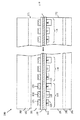
本願発明がその利益を得る方法は、図1を参照すればより容易に理解することができよう。同図は、カラー変換方法に基づく本願発明によるOLEDディスプレイ100の一部分の断面図である。ディスプレイ100は、上述のPET基板材料のようなプラスチック基板161の上に構成される。原色に変換される光をEL層118で発生させる。EL層118における光は、行と列(row and column)並んだ電極群を適当な電源に接続して発生させる。本議論の目的のため、行(row)電極群117をデバイスの陽極と仮定し、列(column)電極群を陰極と仮定する。図1に示した断面図は、1つの行電極に沿って画いたものである。列電極群は、行電極群に対して直角に走っている。代表的な列電極群を131-133で示す。行及び列電極の交差点で発生された光は、列電極の下にあるカラー変換ストリップを照射する。電極群131-133に対応するカラー変換ストリップを、それぞれ、121-123で示す。ストリップ121は、層118によって放射された光を青色光に変換する。同様に、ストリップ122は放射光を緑色に変換し、そしてストリップ123は放射光を赤色に変換する。図1に示したディスプレイ部分は、113-115で示された3つの完全カラーピクセルに対する列電極群を包含している。
【0011】
光を放射させる種々の有機層及び注入層は、パターン化した陽極電極群の上に堆積させる。図面を簡略化するため、これらの層は、単一の発光層118として示されているが、層118は、上述のようにEL層中への正孔及び電子の注入を助長する多数の補助層から構成してもよい、ということは理解すべきである。そのような多層構造の作製は、当分野では一般に行われている故、ここでは詳述しない。選択した特定の材料系に依存して、スピンコーティング、染料昇華(dye sublimation)、ウェブコーティング、又は種々の"印刷"技術によって当該層を堆積させることができる、ということに触れれば十分である。
【0012】
陰極のラインは、カルシウム又はマグネシウムのような低仕事関数の材料から作られる。そのような電極を堆積するためのシャドウマスク形成技術も当分野で周知であり、従って、ここでは詳述しない。
【0013】
上述のように、最終的ディスプレイは、カプセル封止して、酸素や湿気が陰極電極群及び発光層に浸透しないようにしなければならない。当該カプセル封止層を図1の171及び172で示す。本願発明では、カプセル封止層は、上述したものと類似のPML層のように構成される。各カプセル封止層は、2つのポリマー層と、それらの間にサンドイッチ状に挟まれた無機酸化物又は窒化物の層とを含む。カプセル封止層171に対応するポリマー層を、それぞれ、181及び183で示す。カプセル封止層171に対応する酸化物又は窒化物の層を182で示す。同様に、カプセル封止層172に対応するポリマーと酸化物又は窒化物の層を、それぞれ、191、193、及び192で示す。
【0014】
ポリマー層は、そのポリマーのモノマーを、典型的には減圧されている、コーティングチャンバー中に気化させて堆積させる。被覆されるデバイス部分は、その部分を、冷却表面、典型的には、コーティング工程中デバイスがその上を移動しているローラに接触させて、そのモノマーの沸点を下回る温度に維持する。そのモノマー溶媒は、デバイス上に凝縮して、様々な空隙をふさぎ、それによって、表面を平坦化する均一な液体被覆を形成する。その後、モノマーは、UVランプのような放射源への露光によって架橋される。ポリマー層の堆積は、ここに参考として参照されている、上述の引用した特許に詳細に議論されており、従ってここではさらに詳細には議論しない。生ずるポリマー表面は、非常に平滑であるということを書き留めれば十分である。
【0015】
無機酸化物は、重合ポリマー表面上に付ける。PML技術を利用する従来技術のカプセル封止系では、酸化物は、スパッタリング又は蒸着によって付けられた。極端に平滑なポリマー表面は、酸化物を付着できる低欠陥表面をもたらす。従って、その酸化物は、酸素又は水がそれを通して移動できるピンホールが比較的微細である。しかし、酸化物の層は、それでも、デバイスの寿命を限定するくらい十分な酸素又は水を通す。本願発明は、この問題を解決することにある。
【0016】
酸化物の層の浸透度は、層にあるピンホールの密度と酸化物材料の密度の両方で決められる。PML技術はピンホール問題を扱う。但し、従来技術で利用される堆積技術では、浸透度を所望レベルに限定できるくらい十分な濃度の酸化物の層は形成されない。本願発明は、高密度プラズマ、特に電子サイクロトロン共鳴源を利用しているプラズマ拡張気相成長法(ECR-PECVD)によって堆積された酸化物又は窒化物の層は、下側のポリマー層を損傷しない条件下での堆積を可能にする一方、従来技術で教示された方法で堆積されたものより著しく高密度を有するという観察に基づいている。
【0017】
高密度プラズマは、プラズマを含んでいる表面で、eV単位での電子温度の5倍の大きさの極めて小さいシース電圧を有するとして特色付けられる。これは、壁の近傍で容量結合と高シース電圧を有する低密度プラズマとは対照的である。容量性プラズマでは、プラズマへの電力は、壁を叩くイオンの電位に結合される。高密度プラズマでは、壁を叩くイオンの電位は、本質的に極めて低く且つ基板の容量結合電力を加えることにより制御することができる。故に、高密度プラズマによって、被覆されるべき表面で作られる高速の反応性物質と共に、高速の低エネルギーイオンが生成される。これによって、ポリマー類と適合した温度で有用な誘電体の堆積が可能となる。窒化ケイ素、二酸化ケイ素、酸化アルミニウム、炭化ケイ素、オキシ窒化ケイ素、等のような誘電体は、この技術を利用して堆積させることができる。
【0018】
多くの高密度プラズマシステムが使用できる。例えば、前述のシステムは、PlasmaQuest、Plasma-Therm、Surface Technology Systems、Trikon、Lam Research、Applied Materials、Tegal及びNovellusから購入することができる。
【0019】
ECRは、高密度プラズマを作り出す必要がなく、Inductively Coupled Plasma、Helical Resonator、及びHeliconプラズマのようなその他の方式が市販されている。説明だけの一例として、700 Wattsの2.45 GHzマイクロウェーブ電力と約875Gaussの磁界を有し、5〜10 mTorr間の圧力のソースガスとしてシラン、アルゴン及び窒素を使用するOxford InstrumentsのECRシステムは、下述のような優れた結果をもたらすことを筆者達は見出している。これらの動作パラメータは、当業者に明らかになるように、相当に変化させて、特定の基板に対する条件を最適化することができる。
【0020】
本願発明を立証するため、ガラス上の(カルシウムの熱蒸着によって作成した、約200オングストロームの)薄いカルシウム膜上に、この方法によって窒化ケイ素膜を堆積した。膜の温度は、冷却ステージを使って80℃以下に維持した。カルシウムは透明ではないが、空気にさらされると透明な酸化カルシウムに変わる。そのためピンホールに隣接した金属は透明になり、且つその透明な直径は、時間とともに徐々に大きくなった。しかし、残りの金属は、20日後の顕微鏡観察では外見上変化がなかった。わずか1%のカルシウムの反応が酸化しても表面のピンホールが観測できるので、この観察によって、酸化窒化層の浸透率を計算できる。その結果、約8 x 10⁻⁷ moles H2O/m2 dayという浸透率が与えられた。
また、別の本実施例において、その形態的特性の適切な尺度である容積で10%の水性HF溶液における膜のエッチ速度は、120 nm/min.であった。このエッチング速度は水の浸透度を測定できるパラメータとなることが知られている。詳細は、Y.Tessier, et al.,Mat.Res.Soc.Symp.Proc.Vol.86,1986,p.183を参照。この中に示されるデータに基き計算すると、有機LEDに要求されるものより40倍優れた約1 x 10⁻⁸ mols H2O/m2 dayの水浸透度を表すものが生成できた。
【0021】
本願発明のさらに重要な利点は、マイクロウェーブ電力とガス圧のようなパラメータに依存して、堆積無機膜の応力を変え得るということである。軽減された応力は、パターン化素子の歪みを軽減すると共に、ロールツーロール処理中に基板が巻き取られる際の薄層裂け(delamination)又は歪みの発生を防止する。例の膜の応力は、2.5 x 10⁻⁹ dynes/cm2 であった。これは全く低いものである。
【0022】
本願発明のさらに別の利点は、上述の従来技術の方法より改善された堆積速度である。本願発明の方法を使えば、1ミクロン/分を越える速度を達成することができる。堆積速度は、ロールツーロール処理装置が動作できる最大速度を決める故、本願発明によって高スループットを実現することができる。
【0023】
本願発明の好ましい実施例においては、ポリマー層は、約1ミクロン厚のメタクリル酸メチル、ジアクリル酸エチレングリコール、又はその他のアクリル酸塩類、ジアクリル酸塩類、及びトリアクリル酸塩類又はメタクリル酸塩類のような、アクリル系モノマーから構成される。酸化物の層は、好ましくは、350 の厚さをもった窒化ケイ素である。しかし、他の酸化物又は窒化物を使う実施例を構成してもよい。例えば、層182及び192は、酸化ケイ素又は酸化アルミニウム又は窒化アルミニウムから構成することができる。第二ポリマー層は、使用中及び処理中に続いて起こる損傷から窒化物の層を保護するのに使われる。この層はまた、好ましくは、0.25ミクロン以上の厚みを有するアクリル系モノマーから構成する。しかし、両ポリマー層においては、炭酸塩類、フッ素化アルケン類、又は他の液体モノマー類のような、不溶性膜に合わせて硬化させ得るその他のモノマー類を用いてもよい。
【0024】
本願発明の上述の実施例は、陽極電極群がPET基板膜上に置かれたカプセル封止層を説明しているが、PET基板をPML膜でコーティングし、陽極をそのポリマー層上に付けることもできる。一般に、ポリマー層で形成された平滑表面は、PET基板で形成されたそれより優れている。故に、結果として得られる陽極電極群は、PETにITO層を直接付着させて得られる陽極電極群より欠陥が少ない。加えて、ポリマー被覆基板は、別々に作製して保管でき、それによって、OLEDの製造者は、最初のカプセル封止操作を実施する必要がない。
【0025】
本願発明のバリヤー系は、酸素又は水を吸収する層を含めることによってさらに増強させることができる。そのような「ゲッタ」(getter)層は、層に浸透する酸素又は水と反応し、よって、酸素又は水がディスプレイデバイスに達する以前にそれを除去する材料から成る層を設けることによって構成することができる。最も簡単な実施例では、少量のゲッタ化合物を酸化物又は窒化物の層自体に含有させる。例えば、2つのソースからの同時蒸着又は同時スパッタリングによって形成される酸化物又は窒化物に低濃度の金属リチウムを付加することができる。
【0026】
当該層がデバイスの発光側に置かれる場合は、その濃度は、バリヤーの透明度を維持できるほど十分低くなければならない。金属リチウムが消耗し尽くされるまでは、リチウムが酸素又は水と反応し、層の浸透度は、その自由容積が化学結合した酸素原子で占められる故、最初よりも低くなる。故に、デバイスは、ある期間、そうでなければバリヤーに浸透したであろう酸素又は水からさらに一層保護されるであろう。
【0027】
あるいは、ゲッタ層を、図2の200に示すような分離層としてバリヤーとデバイスの間に置いてもよい。この場合、ゲッタ材料から成る分離層201は、PMLバリヤー層202とディスプレー203の間に置かれる。補助的ポリマー層204を用いてゲッタ層をデバイスから分離してもよい。類似構造をデバイスの他面側にも施して酸素及び/又は水がその面から浸透するのを同様に防御する。PML平滑層は、従来技術において、例えば、US #5,047,687及び5,059,816に記述されているものに比較してゲッタ層の特性を改善する。ゲッタ材料は、カルシウム、マグネシウム、又は任意のアルカリ金属のような、水と急速に反応する任意の金属であってよい。その金属はPMLをベースとした水/酸素バリヤーによって保護される故、別法では取扱いが困難な高反応性の金属も用いることができる。
【0028】
水又は酸素がOLEDの活性層に達するのを防ぐという点から本願発明のバリヤー系を説明した。しかし、本願発明の方法を、他方式のデバイス又は膜に対して酸素又は水バリヤーを施すのに用いてもよいということは、先の議論から当業者には明らかであろう。
【0029】
以上、本発明の実施例について詳述したが、以下、本発明の各実施態様の例を示す。
(実施態様1)
水又は酸素がそのソースからデバイス[100, 200]に達するのを防ぐ方法であって、
(a)前記デバイス[100, 200]と前記ソースとの間に第一ポリマー層[191]を堆積するステップと、
(b)前記デバイスの前記第一ポリマー層[191]の上に、ECR-PECVDによって無機層[192]を堆積するステップと、
(c)前記無機層[192]の上に第二ポリマー層[193]を堆積するステップと、
を有することを特徴とする方法。
(実施態様2)
前記無機層[192]が酸化物を含むことを特徴とする請求項1記載の方法。
(実施態様3)
前記酸化物が酸化アルミニウム又は酸化ケイ素を含むことを特徴とする請求項2記載の方法。
(実施態様4)
前記無機層[192]が窒化物を含むことを特徴とする請求項1記載の方法。
(実施態様5)
前記窒化物が窒化アルミニウム又は窒化ケイ素を含むことを特徴とする請求項4記載の方法。
(実施態様6)
前記無機層[192]がオキシ窒化物を含むことを特徴とする請求項1記載の方法。(実施態様7)
前記窒化物が窒化アルミニウム又は窒化ケイ素を含むことを特徴とする請求項6記載の方法。
(実施態様8)
さらに、前記無機層[192]と前記デバイス[100, 200]との間に、酸素又は水を吸収する材料層[201]を堆積するステップを含むことを特徴とする請求項1記載の方法。
(実施態様9)
前記吸収材料が酸化物又は窒化物に均一に分散された金属を含むことを特徴とする請求項8記載の方法。
(実施態様10)
前記無機層[192]が、さらに、酸素又は水を吸収する材料を含むことを特徴とする請求項1記載の方法。
(実施態様11)
前記吸収材料が金属を含むことを特徴とする請求項10記載の方法。
(実施態様12)
電界発光デバイス[100, 200]であって、
(a)第一の波長の光に透明であるフレキシブルシート[161]と、
(b)前記フレキシブルシート[161]と接触している第一ポリマー層[191]と、
(c)前記第一ポリマー層[191]と接触している無機層[192]を含む第一浸透バリヤーと、
(d)前記第一浸透バリヤーに接触している第二ポリマー層[193]と、
(e)前記フレキシブルシート[161]と接触していて、前記の第一の波長の光に透明である第一電極層を含む第一電極[117]と、
(f)前記第一電極層と電気的に接触している有機材料を含む発光層[118]と、
(g)前記発光層[118]と電気的に接触している第二電極層を含む電極であって、前記発光層は前記の第一及び第二電極間に電位差が印加されると前記の第一の波長の光を発生し、
(h)前記第二電極層と接触している第三ポリマー層[181]と、
(i)前記第三ポリマー層と接触している無機材料の層を含む第二浸透バリヤー[182]と、
(j)前記第二浸透バリヤーと接触している第四ポリマー層[183]と、
を含むことを特徴とするデバイス[100, 200]。
(実施態様13)
前記の第一及び第二浸透バリヤーが、ECR-PECVDによって堆積された層を含むことを特徴とする請求項12記載のデバイス[100, 200]。
(実施態様14)
前記第一浸透バリヤーが酸化物を含むことを特徴とする請求項12記載のデバイス[100, 200]。
(実施態様15)
前記酸化物が酸化アルミニウム又は酸化ケイ素を含むことを特徴とする請求項12記載のデバイス[100, 200]。
(実施態様16)
前記第一浸透バリヤーが窒化物を含むことを特徴とする請求項12記載のデバイス[100, 200]。
(実施態様17)
前記窒化物が窒化アルミニウム又は窒化ケイ素を含むことを特徴とする請求項16記載のデバイス[100, 200]。
(実施態様18)
前記の第一及び第二浸透バリヤーが、さらに、酸素又は水を吸収する材料を含むことを特徴とする請求項12記載のデバイス[100, 200]。
(実施態様19)
さらに、酸素又は水を吸収する材料層を含み、前記第一電極層と前記第一浸透バリヤーとの間に配置されている第一吸収層を含むことを特徴とする請求項12記載のデバイス[100, 200]。
(実施態様20)
さらに、酸素又は水を吸収する材料層を含み、前記第二電極層と前記第二浸透バリヤーとの間に配置されている第二吸収層を含むことを特徴とする請求項19記載のデバイス[100, 200]。
【0030】
本願発明に関する種々の変更は、前出の説明並びに添付図面から当業者には明らかとなろう。従って、本願発明は、専ら以下の請求の範囲によってのみ限定されるものである。
【図面の簡単な説明】
【図1】 本願発明によるOLEDディスプレイの一部分の断面図である。
【図2】 酸素又は水の吸収層によってさらに一層保護されているデバイスの断面図である。
【符号の説明】
100、200:デバイス
117:第一電極
118:発光層
161:フレキシブルシート
181:第三ポリマー層
182:第二浸透バリヤー
183:第四ポリマー層
191:第一ポリマー層
192:第一浸透バリヤー
193:第二ポリマー層
201:酸素又は水を吸収する材料層
203:ディスプレー[0001]
BACKGROUND OF THE INVENTION
The present invention relates to electroluminescent devices and, more particularly, to an improved sealing method for organic light emitting displays to extend the life of the display.
[0002]
BACKGROUND OF THE INVENTION
An organic light emitting device (OLED) is a transparent substrate coated with a transparent conductive material, such as indium tin oxide (ITO), one or more organic layers, and Ca or Mg. And a cathode made by vapor deposition or sputtering of a metal having low work function characteristics. The organic layer is selected such that charge can be injected and transmitted from both electrodes into an electroluminescent (EL) organic layer where the charges recombine and emit light. There may be one or more hole transport layers (HTL) between the ITO and the EL, and similarly one or more electron injection and electron transport layers (Electron) between the cathode and the EL. Transport Layer (ETL) may exist.
[0003]
OLED pushes the expectation of providing an inexpensive display. Generally, these devices are built on a flexible substrate using a "roll-to-roll" (roll-to-roll), which is called "roll-to-roll" processing equipment. And can be assembled. For such assembly, inexpensive devices such as polymer film coating devices, metal vaporizers and lithographic devices that can perform the deposition of various layers are already utilized. For example, a polymer thin film web (Web) coating apparatus that is several meters wide can operate at a feed rate of several hundred meters / minute.
[0004]
In order to operate over a long period of time, the OLED must be sealed to prevent water and oxygen from reaching the cathode and polymer layer. Unfortunately, polymers with sufficiently low permeability to water and oxygen are useless. For example, polyethylene terephthalate or PET used as a substrate for web processing has such a high water permeability that the device constructed thereon begins to deteriorate almost immediately due to the reaction between water in the air and the cathode material. Present. Accordingly, certain filler coatings must be applied to the polymer to provide the required resistance to water and oxygen. In addition, the cathode layer must be sealed at the other side of the device to prevent water and oxygen from entering from that side and destroying the cathode.
[0005]
One promising coating technique is the Polymer Multilayer (PML) technique described in US Pat. Nos. 4,842,893, 4,954,371, and 5,260,095. In this technique, a coating consisting of a polymer layer and an aluminum oxide layer is applied to a flexible substrate and the substrate is sealed. Both deposition processes can be operated at very high speeds using web processing equipment. Although the resistance to water and oxygen permeability is improved by 3 to 4 orders of magnitude compared to uncoated PET membranes, the resulting membranes can be used in applications that require several years of life and / or high temperature and humidity. When exposed to the environment, it is likely to penetrate sufficiently to limit the lifetime of the OLED. By using accelerated life testing techniques, it has been shown that in order to have a shelf life of 10 years, its permeability must not exceed about 4 x 10 -7 moles H 2 O / m 2 day. Yes. The best membranes currently available are those that have a permeability that is at least 50 times greater than that. It should be noted that using several polymer bilayers to achieve the required resistance enhancement does not sufficiently improve the resistance to water and oxygen.
[0006]
Broadly speaking, it is an object of the present invention to provide an improved OLED display and a method for manufacturing the same.
[0007]
Another object of the present invention is to provide a method for constructing PML that exhibits sufficient water and oxygen penetration resistance to achieve an OLED having a practically effective lifetime.
[0008]
These and other objects of the present invention will become apparent to those skilled in the art with reference to the following detailed description of the invention and the accompanying drawings.
SUMMARY OF THE INVENTION
[0009]
The present invention is a barrier that prevents water and oxygen from reaching water or oxygen sensitive devices. The barrier is constructed by depositing a first polymer layer between the device and the source. An inorganic layer is deposited on the first polymer layer of the device by plasma enhanced vapor deposition (ECR-PECVD) using an electron cyclotron resonance source. A second polymer layer is then deposited over the inorganic layer. The inorganic layer is preferably an oxide or a nitride. A second barrier layer comprising a water or oxygen absorbing compound may be placed between the inorganic layer and the device to further delay the passage of oxygen or water. The present invention is particularly effective when encapsulating an electroluminescent display.
[0010]
The manner in which the present invention gains its benefits can be more easily understood with reference to FIG. The figure is a cross-sectional view of a portion of an
[0011]
Various organic layers and injection layers that emit light are deposited on the patterned anode group. To simplify the drawings, these layers are shown as a single
[0012]
The cathode line is made from a low work function material such as calcium or magnesium. Shadow mask formation techniques for depositing such electrodes are also well known in the art and are therefore not described in detail here.
[0013]
As described above, the final display must be encapsulated to prevent oxygen and moisture from penetrating the cathode electrode group and the light emitting layer. The encapsulation layer is indicated by 171 and 172 in FIG. In the present invention, the encapsulation layer is configured as a PML layer similar to that described above. Each encapsulation layer includes two polymer layers and an inorganic oxide or nitride layer sandwiched between them. The polymer layers corresponding to the
[0014]
The polymer layer vaporizes and deposits the monomer of the polymer into a coating chamber, typically under reduced pressure. The part of the device to be coated is maintained at a temperature below the boiling point of the monomer by contacting the part with a cooling surface, typically a roller on which the device is moving during the coating process. The monomer solvent condenses on the device and closes various voids, thereby forming a uniform liquid coating that planarizes the surface. The monomer is then crosslinked by exposure to a radiation source such as a UV lamp. The deposition of the polymer layer is discussed in detail in the above cited patents, which are hereby incorporated by reference, and thus will not be discussed in further detail here. It is sufficient to note that the resulting polymer surface is very smooth.
[0015]
The inorganic oxide is applied on the polymerized polymer surface. In prior art encapsulation systems utilizing PML technology, the oxide was applied by sputtering or evaporation. An extremely smooth polymer surface results in a low defect surface on which oxide can be deposited. Thus, the oxide has relatively fine pinholes through which oxygen or water can move. However, the oxide layer still passes enough oxygen or water to limit the lifetime of the device. The present invention is to solve this problem.
[0016]
The permeability of the oxide layer is determined by both the density of pinholes in the layer and the density of the oxide material. PML technology deals with the pinhole problem. However, the deposition technique utilized in the prior art does not form an oxide layer of sufficient concentration to limit the permeability to the desired level. The present invention relates to high density plasmas, particularly oxide or nitride layers deposited by plasma enhanced vapor deposition (ECR-PECVD) utilizing electron cyclotron resonance sources, which do not damage the underlying polymer layer. It is based on the observation that it allows deposition under conditions while having a significantly higher density than that deposited by the methods taught in the prior art.
[0017]
High density plasma is characterized as having a very small sheath voltage on the surface containing the plasma, which is five times the electron temperature in eV. This is in contrast to a low density plasma with capacitive coupling and high sheath voltage near the wall. In capacitive plasma, the power to the plasma is coupled to the potential of the ions that strike the wall. In a high density plasma, the potential of ions hitting the wall is essentially very low and can be controlled by applying capacitive coupling power of the substrate. Thus, the high density plasma produces fast, low energy ions with fast reactive materials created on the surface to be coated. This allows the deposition of useful dielectrics at temperatures compatible with the polymers. Dielectrics such as silicon nitride, silicon dioxide, aluminum oxide, silicon carbide, silicon oxynitride, etc. can be deposited utilizing this technique.
[0018]
Many high density plasma systems can be used. For example, such systems can be purchased from PlasmaQuest, Plasma-Therm, Surface Technology Systems, Trikon, Lam Research, Applied Materials, Tegal and Novellus.
[0019]
ECR does not require the creation of high density plasma, and other schemes such as Inductively Coupled Plasma, Helical Resonator, and Helicon Plasma are commercially available. As an example only, Oxford Instruments' ECR system with 700 Watts 2.45 GHz microwave power and a magnetic field of about 875 Gauss and using silane, argon and nitrogen as source gases at pressures between 5 and 10 mTorr is The authors have found that the results are excellent as described. These operating parameters can be varied considerably to optimize the conditions for a particular substrate, as will be apparent to those skilled in the art.
[0020]
To prove the present invention, a silicon nitride film was deposited by this method on a thin calcium film (about 200 angstroms made by thermal evaporation of calcium) on glass. The temperature of the film was maintained below 80 ° C. using a cooling stage. Calcium is not transparent, but turns into transparent calcium oxide when exposed to air. Therefore, the metal adjacent to the pinhole became transparent, and the transparent diameter gradually increased with time. However, the remaining metals did not change in appearance by microscopic observation after 20 days. Even if the reaction of only 1% of calcium is oxidized, pinholes on the surface can be observed, and this observation can calculate the permeability of the oxynitride layer. As a result, a permeability of about 8 × 10 −7 moles H 2 O / m 2 day was given.
In another example, the etch rate of the film in a 10% aqueous HF solution by volume, which is an appropriate measure of its morphological characteristics, was 120 nm / min. It is known that this etching rate is a parameter that can measure the degree of water penetration. For details, see Y. Tessier, et al., Mat. Res. Soc. Symp. Proc. Vol. 86, 1986, p. 183. Calculations based on the data shown in this figure were able to produce a water permeability of about 1 × 10 −8 mols H 2 O / m 2 day, 40 times better than that required for organic LEDs.
[0021]
A further important advantage of the present invention is that the stress of the deposited inorganic film can be varied depending on parameters such as microwave power and gas pressure. The reduced stress reduces distortion of the patterned element and prevents the occurrence of delamination or distortion when the substrate is rolled up during roll-to-roll processing. The stress of the example film was 2.5 × 10 −9 dynes / cm 2 . This is quite low.
[0022]
Yet another advantage of the present invention is an improved deposition rate over the prior art methods described above. Using the method of the present invention, speeds in excess of 1 micron / minute can be achieved. Since the deposition rate determines the maximum speed at which the roll-to-roll processing apparatus can operate, high throughput can be achieved by the present invention.
[0023]
In a preferred embodiment of the present invention, the polymer layer is about 1 micron thick methyl methacrylate, ethylene glycol diacrylate, or other acrylates, diacrylates, and triacrylates or methacrylates. And composed of acrylic monomers. The oxide layer is preferably silicon nitride with a thickness of 350. However, embodiments using other oxides or nitrides may be constructed. For example, layers 182 and 192 can be composed of silicon oxide or aluminum oxide or aluminum nitride. The second polymer layer is used to protect the nitride layer from subsequent damage during use and processing. This layer is also preferably composed of an acrylic monomer having a thickness of 0.25 microns or greater. However, in both polymer layers, other monomers that can be cured to the insoluble film, such as carbonates, fluorinated alkenes, or other liquid monomers may be used.
[0024]
The above embodiment of the present invention describes an encapsulation layer in which the anode electrode group is placed on a PET substrate film, but the PET substrate is coated with a PML film and the anode is applied on the polymer layer. You can also. In general, a smooth surface formed with a polymer layer is superior to that formed with a PET substrate. Therefore, the resulting anode electrode group has fewer defects than the anode electrode group obtained by directly depositing the ITO layer on PET. In addition, polymer-coated substrates can be made and stored separately, so that the OLED manufacturer does not need to perform an initial encapsulation operation.
[0025]
The barrier system of the present invention can be further enhanced by including a layer that absorbs oxygen or water. Such a "getter" layer is constructed by providing a layer of material that reacts with oxygen or water penetrating the layer and thus removes it before it reaches the display device. Can do. In the simplest embodiment, a small amount of getter compound is included in the oxide or nitride layer itself. For example, low concentrations of metallic lithium can be added to oxides or nitrides formed by co-evaporation or co-sputtering from two sources.
[0026]
If the layer is placed on the light emitting side of the device, its concentration must be low enough to maintain the transparency of the barrier. Until the metallic lithium is depleted, lithium reacts with oxygen or water, and the permeability of the layer is lower than initially because its free volume is occupied by chemically bonded oxygen atoms. Thus, the device will be even more protected from oxygen or water that would otherwise penetrate the barrier for a period of time.
[0027]
Alternatively, the getter layer may be placed between the barrier and the device as a separation layer as shown at 200 in FIG. In this case, a
[0028]
The barrier system of the present invention has been described in terms of preventing water or oxygen from reaching the active layer of the OLED. However, it will be apparent to those skilled in the art from the foregoing discussion that the method of the present invention may be used to apply oxygen or water barriers to other types of devices or membranes.
[0029]
As mentioned above, although the Example of this invention was explained in full detail, the example of each embodiment of this invention is shown below.
(Embodiment 1)
A method of preventing water or oxygen from reaching its device [100, 200] from its source,
(A) depositing a first polymer layer [191] between the device [100, 200] and the source;
(B) depositing an inorganic layer [192] on the first polymer layer [191] of the device by ECR-PECVD;
(C) depositing a second polymer layer [193] on the inorganic layer [192];
A method characterized by comprising:
(Embodiment 2)
The method of claim 1, wherein the inorganic layer [192] comprises an oxide.
(Embodiment 3)
The method of claim 2, wherein the oxide comprises aluminum oxide or silicon oxide.
(Embodiment 4)
The method of claim 1, wherein the inorganic layer [192] comprises a nitride.
(Embodiment 5)
The method of claim 4, wherein the nitride comprises aluminum nitride or silicon nitride.
(Embodiment 6)
The method of claim 1, wherein the inorganic layer [192] comprises oxynitride. (Embodiment 7)
The method of claim 6, wherein the nitride comprises aluminum nitride or silicon nitride.
(Embodiment 8)
The method of claim 1, further comprising depositing a layer of material [201] that absorbs oxygen or water between the inorganic layer [192] and the device [100, 200].
(Embodiment 9)
9. The method of claim 8, wherein the absorbent material comprises a metal uniformly dispersed in an oxide or nitride.
(Embodiment 10)
The method of claim 1, wherein the inorganic layer [192] further comprises a material that absorbs oxygen or water.
(Embodiment 11)
The method of claim 10, wherein the absorbent material comprises a metal.
(Embodiment 12)
An electroluminescent device [100, 200],
(A) a flexible sheet [161] that is transparent to light of the first wavelength;
(B) a first polymer layer [191] in contact with the flexible sheet [161];
(C) a first permeation barrier comprising an inorganic layer [192] in contact with the first polymer layer [191];
(D) a second polymer layer [193] in contact with the first permeation barrier;
(E) a first electrode [117] that is in contact with the flexible sheet [161] and includes a first electrode layer that is transparent to the light of the first wavelength;
(F) a light emitting layer [118] comprising an organic material in electrical contact with the first electrode layer;
(G) an electrode including a second electrode layer that is in electrical contact with the light emitting layer [118], wherein the light emitting layer has the above-mentioned characteristics when a potential difference is applied between the first and second electrodes. Generate light of the first wavelength,
(H) a third polymer layer [181] in contact with the second electrode layer;
(I) a second infiltration barrier [182] comprising a layer of inorganic material in contact with the third polymer layer;
(J) a fourth polymer layer [183] in contact with the second infiltration barrier;
A device characterized by comprising [100, 200].
(Embodiment 13)
13. The device [100, 200] of claim 12, wherein the first and second infiltration barriers comprise layers deposited by ECR-PECVD.
(Embodiment 14)
13. The device [100, 200] of claim 12, wherein the first infiltration barrier comprises an oxide.
(Embodiment 15)
Device [100, 200] according to claim 12, characterized in that the oxide comprises aluminum oxide or silicon oxide.
(Embodiment 16)
The device [100, 200] of claim 12, wherein the first infiltration barrier comprises a nitride.
(Embodiment 17)
The device [100, 200] of claim 16, wherein the nitride comprises aluminum nitride or silicon nitride.
(Embodiment 18)
13. The device [100, 200] of claim 12, wherein the first and second osmotic barriers further comprise a material that absorbs oxygen or water.
(Embodiment 19)
The device according to claim 12, further comprising a material layer that absorbs oxygen or water, and a first absorption layer disposed between the first electrode layer and the first infiltration barrier. 100, 200].
(Embodiment 20)
The device of claim 19, further comprising a material layer that absorbs oxygen or water, and a second absorbent layer disposed between the second electrode layer and the second infiltration barrier. 100, 200].
[0030]
Various modifications regarding the present invention will become apparent to those skilled in the art from the foregoing description and accompanying drawings. Accordingly, the present invention is limited only by the following claims.
[Brief description of the drawings]
FIG. 1 is a cross-sectional view of a portion of an OLED display according to the present invention.
FIG. 2 is a cross-sectional view of a device that is further protected by an oxygen or water absorbing layer.
[Explanation of symbols]
100, 200: Device
117: First electrode
118: Light emitting layer
161: Flexible sheet
181: Third polymer layer
182: Second penetration barrier
183: Fourth polymer layer
191: First polymer layer
192: First penetration barrier
193: Second polymer layer
201: Material layer that absorbs oxygen or water
203: Display
Claims (8)
前記有機発光デバイスと前記ソースとの間に第1のポリマー層を堆積させるステップと、
前記有機発光デバイスの前記第1のポリマー層の上に、ECR-PECVDによって、前記有機発光デバイスが巻き取られる際の薄層裂け又は歪みの発生が防止される低い応力を有する無機層を堆積させるステップと、
前記無機層の上に、第2のポリマー層を堆積させるステップと
からなり、
前記無機層は、均一に分散された、酸素又は水を吸収する金属を更に含む、方法。 In an organic light emitting device assembled on a flexible substrate by a roll-to-roll method, a method of preventing water or oxygen from reaching the organic light emitting device from its source,
Depositing a first polymer layer between the organic light emitting device and the source;
On the first polymer layer of the organic light emitting device, an ECR-PECVD deposits an inorganic layer having a low stress that prevents the occurrence of thin layer tearing or distortion when the organic light emitting device is wound. Steps,
Depositing a second polymer layer on the inorganic layer, and
The method wherein the inorganic layer further comprises a uniformly dispersed metal that absorbs oxygen or water.
Applications Claiming Priority (2)
| Application Number | Priority Date | Filing Date | Title |
|---|---|---|---|
| US09/126,689 US6146225A (en) | 1998-07-30 | 1998-07-30 | Transparent, flexible permeability barrier for organic electroluminescent devices |
| US126,689 | 1998-07-30 |
Publications (3)
| Publication Number | Publication Date |
|---|---|
| JP2000058258A JP2000058258A (en) | 2000-02-25 |
| JP2000058258A5 JP2000058258A5 (en) | 2006-09-07 |
| JP4985898B2 true JP4985898B2 (en) | 2012-07-25 |
Family
ID=22426201
Family Applications (1)
| Application Number | Title | Priority Date | Filing Date |
|---|---|---|---|
| JP21568499A Expired - Fee Related JP4985898B2 (en) | 1998-07-30 | 1999-07-29 | Osmotic barrier for organic electroluminescent devices |
Country Status (4)
| Country | Link |
|---|---|
| US (1) | US6146225A (en) |
| EP (1) | EP0977469B1 (en) |
| JP (1) | JP4985898B2 (en) |
| DE (1) | DE69911524T2 (en) |
Families Citing this family (222)
| Publication number | Priority date | Publication date | Assignee | Title |
|---|---|---|---|---|
| US6224948B1 (en) | 1997-09-29 | 2001-05-01 | Battelle Memorial Institute | Plasma enhanced chemical deposition with low vapor pressure compounds |
| US7126161B2 (en) | 1998-10-13 | 2006-10-24 | Semiconductor Energy Laboratory Co., Ltd. | Semiconductor device having El layer and sealing material |
| AU1339700A (en) | 1998-11-02 | 2000-05-22 | Presstek, Inc. | Transparent conductive oxides for plastic flat panel displays |
| US6274887B1 (en) | 1998-11-02 | 2001-08-14 | Semiconductor Energy Laboratory Co., Ltd. | Semiconductor device and manufacturing method therefor |
| US7141821B1 (en) * | 1998-11-10 | 2006-11-28 | Semiconductor Energy Laboratory Co., Ltd. | Semiconductor device having an impurity gradient in the impurity regions and method of manufacture |
| US7022556B1 (en) | 1998-11-11 | 2006-04-04 | Semiconductor Energy Laboratory Co., Ltd. | Exposure device, exposure method and method of manufacturing semiconductor device |
| US6277679B1 (en) | 1998-11-25 | 2001-08-21 | Semiconductor Energy Laboratory Co., Ltd. | Method of manufacturing thin film transistor |
| JP3912711B2 (en) * | 1998-11-27 | 2007-05-09 | ローム株式会社 | Organic EL device |
| US6228434B1 (en) | 1998-12-16 | 2001-05-08 | Battelle Memorial Institute | Method of making a conformal coating of a microtextured surface |
| US6268695B1 (en) | 1998-12-16 | 2001-07-31 | Battelle Memorial Institute | Environmental barrier material for organic light emitting device and method of making |
| EP1145338B1 (en) | 1998-12-16 | 2012-12-05 | Samsung Display Co., Ltd. | Environmental barrier material for organic light emitting device and method of making |
| US6274204B1 (en) | 1998-12-16 | 2001-08-14 | Battelle Memorial Institute | Method of making non-linear optical polymer |
| US6228436B1 (en) | 1998-12-16 | 2001-05-08 | Battelle Memorial Institute | Method of making light emitting polymer composite material |
| US6207239B1 (en) | 1998-12-16 | 2001-03-27 | Battelle Memorial Institute | Plasma enhanced chemical deposition of conjugated polymer |
| US6207238B1 (en) * | 1998-12-16 | 2001-03-27 | Battelle Memorial Institute | Plasma enhanced chemical deposition for high and/or low index of refraction polymers |
| US6217947B1 (en) | 1998-12-16 | 2001-04-17 | Battelle Memorial Institute | Plasma enhanced polymer deposition onto fixtures |
| US7697052B1 (en) | 1999-02-17 | 2010-04-13 | Semiconductor Energy Laboratory Co., Ltd. | Electronic view finder utilizing an organic electroluminescence display |
| US6506461B2 (en) | 1999-03-31 | 2003-01-14 | Battelle Memorial Institute | Methods for making polyurethanes as thin films |
| US6358570B1 (en) | 1999-03-31 | 2002-03-19 | Battelle Memorial Institute | Vacuum deposition and curing of oligomers and resins |
| US6680487B1 (en) | 1999-05-14 | 2004-01-20 | Semiconductor Energy Laboratory Co., Ltd. | Semiconductor comprising a TFT provided on a substrate having an insulating surface and method of fabricating the same |
| TW527735B (en) | 1999-06-04 | 2003-04-11 | Semiconductor Energy Lab | Electro-optical device |
| US7288420B1 (en) | 1999-06-04 | 2007-10-30 | Semiconductor Energy Laboratory Co., Ltd. | Method for manufacturing an electro-optical device |
| US8853696B1 (en) | 1999-06-04 | 2014-10-07 | Semiconductor Energy Laboratory Co., Ltd. | Electro-optical device and electronic device |
| US6174613B1 (en) * | 1999-07-29 | 2001-01-16 | Agilent Technologies, Inc. | Method and apparatus for fabricating polymer-based electroluminescent displays |
| US6660409B1 (en) * | 1999-09-16 | 2003-12-09 | Panasonic Communications Co., Ltd | Electronic device and process for producing the same |
| TW516244B (en) | 1999-09-17 | 2003-01-01 | Semiconductor Energy Lab | EL display device and method for manufacturing the same |
| JP3942770B2 (en) * | 1999-09-22 | 2007-07-11 | 株式会社半導体エネルギー研究所 | EL display device and electronic device |
| TW480722B (en) * | 1999-10-12 | 2002-03-21 | Semiconductor Energy Lab | Manufacturing method of electro-optical device |
| US6573652B1 (en) | 1999-10-25 | 2003-06-03 | Battelle Memorial Institute | Encapsulated display devices |
| US6866901B2 (en) | 1999-10-25 | 2005-03-15 | Vitex Systems, Inc. | Method for edge sealing barrier films |
| US6623861B2 (en) | 2001-04-16 | 2003-09-23 | Battelle Memorial Institute | Multilayer plastic substrates |
| US6548912B1 (en) | 1999-10-25 | 2003-04-15 | Battelle Memorial Institute | Semicoductor passivation using barrier coatings |
| US7198832B2 (en) | 1999-10-25 | 2007-04-03 | Vitex Systems, Inc. | Method for edge sealing barrier films |
| US6413645B1 (en) * | 2000-04-20 | 2002-07-02 | Battelle Memorial Institute | Ultrabarrier substrates |
| US20100330748A1 (en) | 1999-10-25 | 2010-12-30 | Xi Chu | Method of encapsulating an environmentally sensitive device |
| JP4776769B2 (en) * | 1999-11-09 | 2011-09-21 | 株式会社半導体エネルギー研究所 | Method for manufacturing light emitting device |
| US6646287B1 (en) | 1999-11-19 | 2003-11-11 | Semiconductor Energy Laboratory Co., Ltd. | Semiconductor device with tapered gate and insulating film |
| US20010053559A1 (en) * | 2000-01-25 | 2001-12-20 | Semiconductor Energy Laboratory Co., Ltd. | Method of fabricating display device |
| US6492026B1 (en) * | 2000-04-20 | 2002-12-10 | Battelle Memorial Institute | Smoothing and barrier layers on high Tg substrates |
| US6465953B1 (en) * | 2000-06-12 | 2002-10-15 | General Electric Company | Plastic substrates with improved barrier properties for devices sensitive to water and/or oxygen, such as organic electroluminescent devices |
| US6867539B1 (en) | 2000-07-12 | 2005-03-15 | 3M Innovative Properties Company | Encapsulated organic electronic devices and method for making same |
| US6605826B2 (en) | 2000-08-18 | 2003-08-12 | Semiconductor Energy Laboratory Co., Ltd. | Light-emitting device and display device |
| US6924594B2 (en) * | 2000-10-03 | 2005-08-02 | Semiconductor Energy Laboratory Co., Ltd. | Light emitting device |
| JP4618862B2 (en) * | 2000-10-30 | 2011-01-26 | 大日本印刷株式会社 | Sealed EL element sealed using a barrier laminate structure |
| US7199527B2 (en) * | 2000-11-21 | 2007-04-03 | Alien Technology Corporation | Display device and methods of manufacturing and control |
| US6537688B2 (en) | 2000-12-01 | 2003-03-25 | Universal Display Corporation | Adhesive sealed organic optoelectronic structures |
| JP2002175881A (en) * | 2000-12-07 | 2002-06-21 | Fuji Photo Film Co Ltd | Luminous element |
| US6614057B2 (en) | 2001-02-07 | 2003-09-02 | Universal Display Corporation | Sealed organic optoelectronic structures |
| US7222981B2 (en) * | 2001-02-15 | 2007-05-29 | Semiconductor Energy Laboratory Co., Ltd. | EL display device and electronic device |
| US6576351B2 (en) | 2001-02-16 | 2003-06-10 | Universal Display Corporation | Barrier region for optoelectronic devices |
| US6822391B2 (en) * | 2001-02-21 | 2004-11-23 | Semiconductor Energy Laboratory Co., Ltd. | Light emitting device, electronic equipment, and method of manufacturing thereof |
| US6624568B2 (en) | 2001-03-28 | 2003-09-23 | Universal Display Corporation | Multilayer barrier region containing moisture- and oxygen-absorbing material for optoelectronic devices |
| US6664137B2 (en) * | 2001-03-29 | 2003-12-16 | Universal Display Corporation | Methods and structures for reducing lateral diffusion through cooperative barrier layers |
| JP2002359071A (en) * | 2001-04-20 | 2002-12-13 | Lg Phillips Lcd Co Ltd | Organic light emitting element |
| KR100415615B1 (en) | 2001-06-13 | 2004-01-24 | 엘지전자 주식회사 | Composition Of Getter And Field Emission Display Using The Same |
| US6692326B2 (en) | 2001-06-16 | 2004-02-17 | Cld, Inc. | Method of making organic electroluminescent display |
| TWI264244B (en) | 2001-06-18 | 2006-10-11 | Semiconductor Energy Lab | Light emitting device and method of fabricating the same |
| TW548860B (en) * | 2001-06-20 | 2003-08-21 | Semiconductor Energy Lab | Light emitting device and method of manufacturing the same |
| US7211828B2 (en) | 2001-06-20 | 2007-05-01 | Semiconductor Energy Laboratory Co., Ltd. | Light emitting device and electronic apparatus |
| JP2003086356A (en) * | 2001-09-06 | 2003-03-20 | Semiconductor Energy Lab Co Ltd | Light emitting device and electronic device |
| TW546857B (en) * | 2001-07-03 | 2003-08-11 | Semiconductor Energy Lab | Light-emitting device, method of manufacturing a light-emitting device, and electronic equipment |
| US7469558B2 (en) | 2001-07-10 | 2008-12-30 | Springworks, Llc | As-deposited planar optical waveguides with low scattering loss and methods for their manufacture |
| TW564471B (en) | 2001-07-16 | 2003-12-01 | Semiconductor Energy Lab | Semiconductor device and peeling off method and method of manufacturing semiconductor device |
| KR100413450B1 (en) | 2001-07-20 | 2003-12-31 | 엘지전자 주식회사 | protecting film structure for display device |
| EP1419286A1 (en) * | 2001-08-20 | 2004-05-19 | Nova-Plasma Inc. | Coatings with low permeation of gases and vapors |
| US6888307B2 (en) * | 2001-08-21 | 2005-05-03 | Universal Display Corporation | Patterned oxygen and moisture absorber for organic optoelectronic device structures |
| TW558743B (en) | 2001-08-22 | 2003-10-21 | Semiconductor Energy Lab | Peeling method and method of manufacturing semiconductor device |
| JP4166455B2 (en) * | 2001-10-01 | 2008-10-15 | 株式会社半導体エネルギー研究所 | Polarizing film and light emitting device |
| US6888305B2 (en) * | 2001-11-06 | 2005-05-03 | Universal Display Corporation | Encapsulation structure that acts as a multilayer mirror |
| US6730373B2 (en) | 2001-11-21 | 2004-05-04 | Optical Coating Laboratory, Inc. | Glass panel with barrier coating and related methods |
| US6597111B2 (en) | 2001-11-27 | 2003-07-22 | Universal Display Corporation | Protected organic optoelectronic devices |
| US7050835B2 (en) * | 2001-12-12 | 2006-05-23 | Universal Display Corporation | Intelligent multi-media display communication system |
| CN100483782C (en) * | 2001-12-13 | 2009-04-29 | 皇家飞利浦电子股份有限公司 | Sealing structure for display devices |
| US6765351B2 (en) * | 2001-12-20 | 2004-07-20 | The Trustees Of Princeton University | Organic optoelectronic device structures |
| US7012363B2 (en) * | 2002-01-10 | 2006-03-14 | Universal Display Corporation | OLEDs having increased external electroluminescence quantum efficiencies |
| US6884327B2 (en) | 2002-03-16 | 2005-04-26 | Tao Pan | Mode size converter for a planar waveguide |
| US7378356B2 (en) | 2002-03-16 | 2008-05-27 | Springworks, Llc | Biased pulse DC reactive sputtering of oxide films |
| US6891330B2 (en) * | 2002-03-29 | 2005-05-10 | General Electric Company | Mechanically flexible organic electroluminescent device with directional light emission |
| US6835950B2 (en) | 2002-04-12 | 2004-12-28 | Universal Display Corporation | Organic electronic devices with pressure sensitive adhesive layer |
| US6897474B2 (en) * | 2002-04-12 | 2005-05-24 | Universal Display Corporation | Protected organic electronic devices and methods for making the same |
| DE10222958B4 (en) * | 2002-04-15 | 2007-08-16 | Schott Ag | Process for producing an organic electro-optical element and organic electro-optical element |
| US8900366B2 (en) | 2002-04-15 | 2014-12-02 | Samsung Display Co., Ltd. | Apparatus for depositing a multilayer coating on discrete sheets |
| US7268486B2 (en) | 2002-04-15 | 2007-09-11 | Schott Ag | Hermetic encapsulation of organic, electro-optical elements |
| US8808457B2 (en) | 2002-04-15 | 2014-08-19 | Samsung Display Co., Ltd. | Apparatus for depositing a multilayer coating on discrete sheets |
| KR100462469B1 (en) * | 2002-04-17 | 2004-12-17 | 한국전자통신연구원 | Encapsulation thin films having bonding-type organic-inorganic complex film and organic electroluminescent devices including the same |
| KR100475849B1 (en) * | 2002-04-17 | 2005-03-10 | 한국전자통신연구원 | Organic electroluminescent devices having encapsulation thin film formed by wet processing and methods for manufacturing the same |
| AU2003219382A1 (en) * | 2002-05-10 | 2003-11-11 | Koninklijke Philips Electronics N.V. | Electroluminescent panel |
| US7164155B2 (en) * | 2002-05-15 | 2007-01-16 | Semiconductor Energy Laboratory Co., Ltd. | Light emitting device |
| US7230271B2 (en) | 2002-06-11 | 2007-06-12 | Semiconductor Energy Laboratory Co., Ltd. | Light emitting device comprising film having hygroscopic property and transparency and manufacturing method thereof |
| KR100819297B1 (en) * | 2002-06-26 | 2008-04-02 | 삼성전자주식회사 | Preparation Method For High Reflective Micropattern |
| KR100484954B1 (en) * | 2002-07-08 | 2005-04-22 | 엘지.필립스 엘시디 주식회사 | encapsulation method of Organic Electro luminescence Device |
| US20070264564A1 (en) | 2006-03-16 | 2007-11-15 | Infinite Power Solutions, Inc. | Thin film battery on an integrated circuit or circuit board and method thereof |
| US8394522B2 (en) | 2002-08-09 | 2013-03-12 | Infinite Power Solutions, Inc. | Robust metal film encapsulation |
| US8404376B2 (en) | 2002-08-09 | 2013-03-26 | Infinite Power Solutions, Inc. | Metal film encapsulation |
| US8021778B2 (en) | 2002-08-09 | 2011-09-20 | Infinite Power Solutions, Inc. | Electrochemical apparatus with barrier layer protected substrate |
| US8445130B2 (en) | 2002-08-09 | 2013-05-21 | Infinite Power Solutions, Inc. | Hybrid thin-film battery |
| US8236443B2 (en) | 2002-08-09 | 2012-08-07 | Infinite Power Solutions, Inc. | Metal film encapsulation |
| US8431264B2 (en) | 2002-08-09 | 2013-04-30 | Infinite Power Solutions, Inc. | Hybrid thin-film battery |
| US9793523B2 (en) | 2002-08-09 | 2017-10-17 | Sapurast Research Llc | Electrochemical apparatus with barrier layer protected substrate |
| US6933051B2 (en) | 2002-08-17 | 2005-08-23 | 3M Innovative Properties Company | Flexible electrically conductive film |
| US7215473B2 (en) * | 2002-08-17 | 2007-05-08 | 3M Innovative Properties Company | Enhanced heat mirror films |
| US6929864B2 (en) * | 2002-08-17 | 2005-08-16 | 3M Innovative Properties Company | Extensible, visible light-transmissive and infrared-reflective film and methods of making and using the film |
| US6818291B2 (en) | 2002-08-17 | 2004-11-16 | 3M Innovative Properties Company | Durable transparent EMI shielding film |
| AU2003261463A1 (en) | 2002-08-27 | 2004-03-19 | Symmorphix, Inc. | Optically coupling into highly uniform waveguides |
| US6994933B1 (en) | 2002-09-16 | 2006-02-07 | Oak Ridge Micro-Energy, Inc. | Long life thin film battery and method therefor |
| CN1176565C (en) * | 2002-11-25 | 2004-11-17 | 清华大学 | Package layer for organic electroluminescent device and its prepn method and application |
| US7710019B2 (en) | 2002-12-11 | 2010-05-04 | Samsung Electronics Co., Ltd. | Organic light-emitting diode display comprising auxiliary electrodes |
| KR20050089971A (en) * | 2002-12-20 | 2005-09-09 | 이화이어 테크놀로지 코포레이션 | Aluminum nitride passivated phosphors for electroluminescent displays |
| WO2004079781A2 (en) * | 2003-03-04 | 2004-09-16 | Dow Corning Corporation | Organic light-emitting diode |
| US20070184181A1 (en) * | 2003-03-25 | 2007-08-09 | Kazuo Wada | Device and method for forming film for organic electro-luminescence element using inductive coupling CVD |
| US7018713B2 (en) | 2003-04-02 | 2006-03-28 | 3M Innovative Properties Company | Flexible high-temperature ultrabarrier |
| US7648925B2 (en) | 2003-04-11 | 2010-01-19 | Vitex Systems, Inc. | Multilayer barrier stacks and methods of making multilayer barrier stacks |
| US7344901B2 (en) * | 2003-04-16 | 2008-03-18 | Corning Incorporated | Hermetically sealed package and method of fabricating of a hermetically sealed package |
| US6998776B2 (en) * | 2003-04-16 | 2006-02-14 | Corning Incorporated | Glass package that is hermetically sealed with a frit and method of fabrication |
| US20040206953A1 (en) * | 2003-04-16 | 2004-10-21 | Robert Morena | Hermetically sealed glass package and method of fabrication |
| US7238628B2 (en) | 2003-05-23 | 2007-07-03 | Symmorphix, Inc. | Energy conversion and storage films and devices by physical vapor deposition of titanium and titanium oxides and sub-oxides |
| US8728285B2 (en) | 2003-05-23 | 2014-05-20 | Demaray, Llc | Transparent conductive oxides |
| US20040238846A1 (en) * | 2003-05-30 | 2004-12-02 | Georg Wittmann | Organic electronic device |
| CA2528837A1 (en) * | 2003-07-07 | 2005-01-13 | Ifire Technology Corp. | Seal and sealing process for electroluminescent displays |
| US6998648B2 (en) * | 2003-08-25 | 2006-02-14 | Universal Display Corporation | Protected organic electronic device structures incorporating pressure sensitive adhesive and desiccant |
| US8722160B2 (en) | 2003-10-31 | 2014-05-13 | Aeris Capital Sustainable Ip Ltd. | Inorganic/organic hybrid nanolaminate barrier film |
| US7495644B2 (en) * | 2003-12-26 | 2009-02-24 | Semiconductor Energy Laboratory Co., Ltd. | Display device and method for manufacturing display device |
| CN1328936C (en) * | 2004-01-05 | 2007-07-25 | 统宝光电股份有限公司 | Method for forming package protective structure |
| DE102004005370B4 (en) * | 2004-02-03 | 2007-08-16 | Samsung SDI Co., Ltd., Suwon | Electrical device with a housing and an OLED display element and method for its production |
| US7202504B2 (en) | 2004-05-20 | 2007-04-10 | Semiconductor Energy Laboratory Co., Ltd. | Light-emitting element and display device |
| DE102004026618A1 (en) * | 2004-06-01 | 2005-12-29 | Siemens Ag | X-ray detector |
| US20050269943A1 (en) * | 2004-06-04 | 2005-12-08 | Michael Hack | Protected organic electronic devices and methods for making the same |
| US7812522B2 (en) * | 2004-07-22 | 2010-10-12 | Ifire Ip Corporation | Aluminum oxide and aluminum oxynitride layers for use with phosphors for electroluminescent displays |
| US20090032108A1 (en) * | 2007-03-30 | 2009-02-05 | Craig Leidholm | Formation of photovoltaic absorber layers on foil substrates |
| US20060063015A1 (en) * | 2004-09-23 | 2006-03-23 | 3M Innovative Properties Company | Protected polymeric film |
| US7342356B2 (en) * | 2004-09-23 | 2008-03-11 | 3M Innovative Properties Company | Organic electroluminescent device having protective structure with boron oxide layer and inorganic barrier layer |
| US20060093795A1 (en) * | 2004-11-04 | 2006-05-04 | Eastman Kodak Company | Polymeric substrate having a desiccant layer |
| DE602005017512D1 (en) | 2004-12-08 | 2009-12-17 | Symmorphix Inc | DEPOSIT OF LICOO2 |
| US7959769B2 (en) | 2004-12-08 | 2011-06-14 | Infinite Power Solutions, Inc. | Deposition of LiCoO2 |
| US20060153997A1 (en) * | 2005-01-07 | 2006-07-13 | Eastman Kodak Company | Method of varying wavelengths of liquid crystals |
| DE112006000279B4 (en) * | 2005-01-14 | 2014-06-05 | Kyoto University | USE OF A GAS ABSORBENT SUBSTANCE AND A GAS ABSORBENT ALLOY |
| KR100623731B1 (en) * | 2005-03-16 | 2006-09-14 | 삼성에스디아이 주식회사 | Organic light emitting display and method of fabricating the same |
| US20070020451A1 (en) | 2005-07-20 | 2007-01-25 | 3M Innovative Properties Company | Moisture barrier coatings |
| ITMI20051502A1 (en) * | 2005-07-29 | 2007-01-30 | Getters Spa | GETTER SYSTEMS INCLUDING ONE OR MORE DEPOSITS OF GETTER MATERIAL AND A LAYER OF MATERIAL FOR H02O TRANSPORT |
| US7829147B2 (en) | 2005-08-18 | 2010-11-09 | Corning Incorporated | Hermetically sealing a device without a heat treating step and the resulting hermetically sealed device |
| US7722929B2 (en) | 2005-08-18 | 2010-05-25 | Corning Incorporated | Sealing technique for decreasing the time it takes to hermetically seal a device and the resulting hermetically sealed device |
| US20070040501A1 (en) | 2005-08-18 | 2007-02-22 | Aitken Bruce G | Method for inhibiting oxygen and moisture degradation of a device and the resulting device |
| US7767498B2 (en) | 2005-08-25 | 2010-08-03 | Vitex Systems, Inc. | Encapsulated devices and method of making |
| US7838133B2 (en) | 2005-09-02 | 2010-11-23 | Springworks, Llc | Deposition of perovskite and other compound ceramic films for dielectric applications |
| US8193705B2 (en) * | 2005-11-02 | 2012-06-05 | Ifire Ip Corporation | Laminated conformal seal for electroluminescent displays |
| US7537504B2 (en) * | 2005-12-06 | 2009-05-26 | Corning Incorporated | Method of encapsulating a display element with frit wall and laser beam |
| US7597603B2 (en) * | 2005-12-06 | 2009-10-06 | Corning Incorporated | Method of encapsulating a display element |
| JP4539547B2 (en) * | 2005-12-08 | 2010-09-08 | セイコーエプソン株式会社 | LIGHT EMITTING DEVICE, LIGHT EMITTING DEVICE MANUFACTURING METHOD, AND ELECTRONIC DEVICE |
| US20070131944A1 (en) * | 2005-12-08 | 2007-06-14 | Au Optronics Corporation | Dual organic electroluminescent display and method of making same |
| US8044571B2 (en) * | 2005-12-14 | 2011-10-25 | General Electric Company | Electrode stacks for electroactive devices and methods of fabricating the same |
| US8158450B1 (en) * | 2006-05-05 | 2012-04-17 | Nanosolar, Inc. | Barrier films and high throughput manufacturing processes for photovoltaic devices |
| US20080006819A1 (en) * | 2006-06-19 | 2008-01-10 | 3M Innovative Properties Company | Moisture barrier coatings for organic light emitting diode devices |
| US20080124558A1 (en) * | 2006-08-18 | 2008-05-29 | Heather Debra Boek | Boro-silicate glass frits for hermetic sealing of light emitting device displays |
| US20080048178A1 (en) | 2006-08-24 | 2008-02-28 | Bruce Gardiner Aitken | Tin phosphate barrier film, method, and apparatus |
| WO2008039471A2 (en) | 2006-09-29 | 2008-04-03 | Infinite Power Solutions, Inc. | Masking of and material constraint for depositing battery layers on flexible substrates |
| DE102006048339A1 (en) * | 2006-10-12 | 2008-04-24 | Agfaphoto Gmbh | Protective film for reducing exposure to substance comprises flexible support to which layer having low permeability to substance, layer that reduces free substance content and another layer having low permeability to substance, are applied |
| US20080100202A1 (en) * | 2006-11-01 | 2008-05-01 | Cok Ronald S | Process for forming oled conductive protective layer |
| US8197781B2 (en) | 2006-11-07 | 2012-06-12 | Infinite Power Solutions, Inc. | Sputtering target of Li3PO4 and method for producing same |
| US8115326B2 (en) | 2006-11-30 | 2012-02-14 | Corning Incorporated | Flexible substrates having a thin-film barrier |
| JP5519293B2 (en) | 2006-12-28 | 2014-06-11 | スリーエム イノベイティブ プロパティズ カンパニー | Nucleation layer for thin metal layer formation |
| CN101573471A (en) * | 2006-12-29 | 2009-11-04 | 3M创新有限公司 | Method of curing metal alkoxide-containing films |
| KR20150015013A (en) * | 2006-12-29 | 2015-02-09 | 쓰리엠 이노베이티브 프로퍼티즈 컴파니 | Method of making inorganic or inorganic/organic hybrid films |
| NL1033860C2 (en) | 2007-05-16 | 2008-11-18 | Otb Group Bv | Method for applying a thin film encapsulation layer assembly to an organic device and an organic device provided with a thin film encapsulation layer assembly preferably applied by such a method. |
| JP5208591B2 (en) | 2007-06-28 | 2013-06-12 | 株式会社半導体エネルギー研究所 | Light emitting device and lighting device |
| WO2009033096A2 (en) | 2007-09-07 | 2009-03-12 | Avery Dennison Corporation | Block out label, label sheet, and related method |
| WO2009053886A2 (en) * | 2007-10-25 | 2009-04-30 | Koninklijke Philips Electronics N.V. | Organic electro-optical device, light source, display device and solar cell |
| US20090162667A1 (en) * | 2007-12-20 | 2009-06-25 | Lumination Llc | Lighting device having backlighting, illumination and display applications |
| US8268488B2 (en) | 2007-12-21 | 2012-09-18 | Infinite Power Solutions, Inc. | Thin film electrolyte for thin film batteries |
| TWI441937B (en) | 2007-12-21 | 2014-06-21 | Infinite Power Solutions Inc | Method for sputter targets for electrolyte films |
| KR100832847B1 (en) * | 2007-12-21 | 2008-05-28 | (주)누리셀 | Multi layer for encapsulation comprising a planarizing organic thin layer and a comformal organic thin layer |
| CN101945965A (en) | 2007-12-28 | 2011-01-12 | 3M创新有限公司 | Flexible package film system |
| KR101606183B1 (en) | 2008-01-11 | 2016-03-25 | 사푸라스트 리써치 엘엘씨 | Thin film encapsulation for thin film batteries and other devices |
| KR101672254B1 (en) | 2008-04-02 | 2016-11-08 | 사푸라스트 리써치 엘엘씨 | Passive over/under voltage control and protection for energy storage devices associated with energy harvesting |
| US8053984B2 (en) * | 2008-05-26 | 2011-11-08 | Lg Display Co., Ltd. | Organic light emitting diode display |
| US8350451B2 (en) | 2008-06-05 | 2013-01-08 | 3M Innovative Properties Company | Ultrathin transparent EMI shielding film comprising a polymer basecoat and crosslinked polymer transparent dielectric layer |
| US8448468B2 (en) | 2008-06-11 | 2013-05-28 | Corning Incorporated | Mask and method for sealing a glass envelope |
| EP2304069A4 (en) * | 2008-06-30 | 2012-01-04 | 3M Innovative Properties Co | Method of making inorganic or inorganic/organic hybrid barrier films |
| CN102119454B (en) | 2008-08-11 | 2014-07-30 | 无穷动力解决方案股份有限公司 | Energy device with integral collector surface for electromagnetic energy harvesting and method thereof |
| KR101613671B1 (en) | 2008-09-12 | 2016-04-19 | 사푸라스트 리써치 엘엘씨 | Energy device with integral conductive surface for data communication via electromagnetic energy and method thereof |
| US8508193B2 (en) | 2008-10-08 | 2013-08-13 | Infinite Power Solutions, Inc. | Environmentally-powered wireless sensor module |
| JP2011003522A (en) | 2008-10-16 | 2011-01-06 | Semiconductor Energy Lab Co Ltd | Flexible light-emitting device, electronic equipment, and method of manufacturing flexible light-emitting device |
| US20100095705A1 (en) | 2008-10-20 | 2010-04-22 | Burkhalter Robert S | Method for forming a dry glass-based frit |
| US9337446B2 (en) | 2008-12-22 | 2016-05-10 | Samsung Display Co., Ltd. | Encapsulated RGB OLEDs having enhanced optical output |
| US9184410B2 (en) | 2008-12-22 | 2015-11-10 | Samsung Display Co., Ltd. | Encapsulated white OLEDs having enhanced optical output |
| US8219408B2 (en) * | 2008-12-29 | 2012-07-10 | Motorola Mobility, Inc. | Audio signal decoder and method for producing a scaled reconstructed audio signal |
| US9099679B2 (en) * | 2009-06-01 | 2015-08-04 | Sumitomo Chemical Company Limited | Encapsulation process and structure for electronic devices |
| US8766269B2 (en) * | 2009-07-02 | 2014-07-01 | Semiconductor Energy Laboratory Co., Ltd. | Light-emitting device, lighting device, and electronic device |
| US8599572B2 (en) | 2009-09-01 | 2013-12-03 | Infinite Power Solutions, Inc. | Printed circuit board with integrated thin film battery |
| US8580332B2 (en) * | 2009-09-22 | 2013-11-12 | Applied Materials, Inc. | Thin-film battery methods for complexity reduction |
| US9472783B2 (en) * | 2009-10-12 | 2016-10-18 | General Electric Company | Barrier coating with reduced process time |
| CN101707237B (en) * | 2009-10-30 | 2011-08-17 | 彩虹集团公司 | Packaging structure and packing method of flexible organic electroluminescent device |
| US8590338B2 (en) | 2009-12-31 | 2013-11-26 | Samsung Mobile Display Co., Ltd. | Evaporator with internal restriction |
| KR101155904B1 (en) | 2010-01-04 | 2012-06-20 | 삼성모바일디스플레이주식회사 | Organic light emitting diode display |
| US9000442B2 (en) * | 2010-01-20 | 2015-04-07 | Semiconductor Energy Laboratory Co., Ltd. | Light-emitting device, flexible light-emitting device, electronic device, and method for manufacturing light-emitting device and flexible-light emitting device |
| TWI589042B (en) * | 2010-01-20 | 2017-06-21 | 半導體能源研究所股份有限公司 | Light-emitting device, flexible light-emitting device, electronic device, lighting apparatus, and method of manufacturing light-emitting device and flexible-light emitting device |
| US20110300432A1 (en) | 2010-06-07 | 2011-12-08 | Snyder Shawn W | Rechargeable, High-Density Electrochemical Device |
| TWI540939B (en) | 2010-09-14 | 2016-07-01 | 半導體能源研究所股份有限公司 | Solid-state light-emitting element, light-emitting device, and lighting device |
| JP5827104B2 (en) | 2010-11-19 | 2015-12-02 | 株式会社半導体エネルギー研究所 | Lighting device |
| TWI562422B (en) | 2010-12-16 | 2016-12-11 | Semiconductor Energy Lab Co Ltd | Light-emitting device and lighting device |
| US8735874B2 (en) | 2011-02-14 | 2014-05-27 | Semiconductor Energy Laboratory Co., Ltd. | Light-emitting device, display device, and method for manufacturing the same |
| KR101922603B1 (en) | 2011-03-04 | 2018-11-27 | 가부시키가이샤 한도오따이 에네루기 켄큐쇼 | Light-emitting device, lighting device, substrate, and manufacturing method of substrate |
| KR101308480B1 (en) * | 2011-06-14 | 2013-09-16 | 엘지디스플레이 주식회사 | Plastic organic light emitting display panel and method of fabricating the same |
| JP5504221B2 (en) * | 2011-08-05 | 2014-05-28 | 株式会社半導体エネルギー研究所 | Light emitting device and manufacturing method thereof |
| KR102079188B1 (en) | 2012-05-09 | 2020-02-19 | 가부시키가이샤 한도오따이 에네루기 켄큐쇼 | Light-emitting device and electronic device |
| KR101951223B1 (en) | 2012-10-26 | 2019-02-25 | 삼성디스플레이 주식회사 | Display device and method of manufacturing the same |
| KR102309244B1 (en) | 2013-02-20 | 2021-10-05 | 가부시키가이샤 한도오따이 에네루기 켄큐쇼 | Semiconductor device |
| EP2979859A4 (en) | 2013-03-27 | 2016-11-02 | Toppan Printing Co Ltd | Laminate and gas barrier film |
| KR102084715B1 (en) | 2013-06-18 | 2020-03-05 | 삼성디스플레이 주식회사 | Organic light emitting diode display panel |
| WO2015087192A1 (en) | 2013-12-12 | 2015-06-18 | Semiconductor Energy Laboratory Co., Ltd. | Peeling method and peeling apparatus |
| CN104746036B (en) * | 2013-12-31 | 2017-11-07 | 中国科学院微电子研究所 | A kind of film encapsulation method |
| EP3186319A4 (en) | 2014-07-25 | 2018-04-18 | Kateeva, Inc. | Organic thin film ink compositions and methods |
| US9923176B2 (en) | 2015-04-08 | 2018-03-20 | Stmicroelectronics (Tours) Sas | Power unit using flexible conductive member |
| CN105098090A (en) * | 2015-06-15 | 2015-11-25 | 深圳市华星光电技术有限公司 | Package structure and package method of organic light-emitting diode (OLED) device |
| CN107922766A (en) | 2015-08-31 | 2018-04-17 | 科迪华公司 | Organic film ink composite based on two and single (methyl) acrylate |
| JP6457371B2 (en) * | 2015-10-09 | 2019-01-23 | 富士フイルム株式会社 | Gas barrier film, organic electronic device, substrate for organic electroluminescent device, organic electroluminescent device |
| US20180309089A1 (en) | 2017-04-21 | 2018-10-25 | Kateeva, Inc. | Compositions and Techniques for Forming Organic Thin Films |
| WO2018226078A1 (en) * | 2017-06-09 | 2018-12-13 | 주식회사 엘지화학 | Sealing film |
| CN107369776B (en) | 2017-08-18 | 2020-05-08 | 京东方科技集团股份有限公司 | Packaging structure of OLED device and OLED device |
| CN109904345A (en) * | 2019-02-28 | 2019-06-18 | 武汉华星光电半导体显示技术有限公司 | Encapsulating structure and its display device |
| US11588137B2 (en) | 2019-06-05 | 2023-02-21 | Semiconductor Energy Laboratory Co., Ltd. | Functional panel, display device, input/output device, and data processing device |
| US11659758B2 (en) | 2019-07-05 | 2023-05-23 | Semiconductor Energy Laboratory Co., Ltd. | Display unit, display module, and electronic device |
| US11844236B2 (en) | 2019-07-12 | 2023-12-12 | Semiconductor Energy Laboratory Co., Ltd. | Functional panel, display device, input/output device, and data processing device |
Family Cites Families (22)
| Publication number | Priority date | Publication date | Assignee | Title |
|---|---|---|---|---|
| US4842893A (en) * | 1983-12-19 | 1989-06-27 | Spectrum Control, Inc. | High speed process for coating substrates |
| US4954371A (en) * | 1986-06-23 | 1990-09-04 | Spectrum Control, Inc. | Flash evaporation of monomer fluids |
| JPS6354295U (en) * | 1986-09-26 | 1988-04-12 | ||
| DE68921707T2 (en) * | 1988-12-05 | 1995-08-10 | Mitsubishi Chem Corp | Waterproof film. |
| JP2820469B2 (en) * | 1988-12-05 | 1998-11-05 | 三菱化学株式会社 | Moisture proof film |
| US5346752A (en) * | 1990-10-17 | 1994-09-13 | Mitsubishi Kasei Corporation | Heat-resistant moistureproof film |
| JP3020692B2 (en) * | 1990-10-17 | 2000-03-15 | 三菱化学株式会社 | Heat resistant moisture proof film |
| US5260095A (en) * | 1992-08-21 | 1993-11-09 | Battelle Memorial Institute | Vacuum deposition and curing of liquid monomers |
| JP3192249B2 (en) * | 1992-10-27 | 2001-07-23 | 鐘淵化学工業株式会社 | Gas and moisture barrier film and method for producing the same |
| JP3277965B2 (en) * | 1993-09-20 | 2002-04-22 | 東洋紡績株式会社 | Electroluminescence panel |
| JP3577117B2 (en) * | 1994-10-07 | 2004-10-13 | Tdk株式会社 | Manufacturing method of organic electroluminescence device |
| JP3261945B2 (en) * | 1994-10-14 | 2002-03-04 | 東洋インキ製造株式会社 | Electroluminescent element sealing laminate and electroluminescent element sealing structure |
| JPH0917572A (en) * | 1995-06-26 | 1997-01-17 | Hewlett Packard Co <Hp> | Seal formation of thin-film electroluminescence element and electroluminescence element |
| JP3900543B2 (en) * | 1995-07-17 | 2007-04-04 | 東洋紡績株式会社 | Laminated film |
| JP3539597B2 (en) * | 1995-10-13 | 2004-07-07 | ソニー株式会社 | Organic optical element and method of manufacturing the same |
| US5811177A (en) * | 1995-11-30 | 1998-09-22 | Motorola, Inc. | Passivation of electroluminescent organic devices |
| JPH09151371A (en) * | 1995-11-30 | 1997-06-10 | Toppan Printing Co Ltd | Organic thin film el element |
| US5686360A (en) * | 1995-11-30 | 1997-11-11 | Motorola | Passivation of organic devices |
| JP2950240B2 (en) * | 1996-06-24 | 1999-09-20 | 関西日本電気株式会社 | Electroluminescent lamp |
| JP3620186B2 (en) * | 1996-12-12 | 2005-02-16 | 凸版印刷株式会社 | Organic thin film EL device |
| JPH10275680A (en) * | 1997-03-31 | 1998-10-13 | Toyota Central Res & Dev Lab Inc | Organic el element |
| AU6853898A (en) * | 1997-04-17 | 1998-11-11 | Kureha Kagaku Kogyo K.K. | Moisture-proofing film and electroluminescent device |
-
1998
- 1998-07-30 US US09/126,689 patent/US6146225A/en not_active Expired - Lifetime
-
1999
- 1999-07-29 JP JP21568499A patent/JP4985898B2/en not_active Expired - Fee Related
- 1999-07-30 EP EP99114946A patent/EP0977469B1/en not_active Expired - Lifetime
- 1999-07-30 DE DE69911524T patent/DE69911524T2/en not_active Expired - Fee Related
Also Published As
| Publication number | Publication date |
|---|---|
| JP2000058258A (en) | 2000-02-25 |
| EP0977469B1 (en) | 2003-09-24 |
| DE69911524T2 (en) | 2004-07-15 |
| DE69911524D1 (en) | 2003-10-30 |
| EP0977469A2 (en) | 2000-02-02 |
| EP0977469A3 (en) | 2000-09-20 |
| US6146225A (en) | 2000-11-14 |
Similar Documents
| Publication | Publication Date | Title |
|---|---|---|
| JP4985898B2 (en) | Osmotic barrier for organic electroluminescent devices | |
| US7077935B2 (en) | O2 and H2O barrier material | |
| US9203052B2 (en) | Organic light emitting diode display and method of manufacturing the same | |
| US7704677B2 (en) | Method of patterning conductive polymer layer, organic light emitting device, and method of manufacturing the organic light emitting device | |
| US8268650B2 (en) | Process for manufacturing sealed organic electroluminescence devices | |
| JP2003017244A (en) | Organic electroluminescent element and its manufacturing method | |
| JP2004071549A (en) | Organic light emitting device and manufacturing method | |
| KR20060084743A (en) | Method for making organic electric light emission device having thin film encapsulation | |
| JP4810739B2 (en) | Organic electroluminescence device and method for producing the same | |
| JP2012512327A (en) | Method for forming an insulating layer with particles having low energy | |
| KR20010067868A (en) | Organic Light-Emitting Device excellent in endurance and the method of manufacturing the same | |
| JP4337567B2 (en) | Method for manufacturing organic electroluminescence element | |
| JP4543691B2 (en) | Organic electroluminescence device and method for producing the same | |
| KR19990012364A (en) | Structure of Polymer / Organic Electroluminescent Device Using Ionomer as Charge Transport Layer and Manufacturing Method Thereof | |
| JP2004014287A (en) | Ito film, its manufacturing method and organic el element | |
| US20080268136A1 (en) | Method of producing organic light emitting apparatus | |
| JP2004050821A (en) | Steam permeation preventing membrane and its manufacturing method | |
| TW200901818A (en) | Method of producing organic light emitting apparatus | |
| WO2015027606A1 (en) | Thin-film, manufacturing method therfor, and light-emitting display component | |
| JP2003249379A (en) | Surface treatment method for transparent conductive film, transparent conductive film with surface modified by using the same, and charge injection luminescence element having surface modified transparent conductive film | |
| Han et al. | Improvement of permeation of solvent-free multilayer encapsulation of thin films on poly (ethylene terephthalate) | |
| JP2013089561A (en) | Organic el device and method of manufacturing organic el device | |
| JP4747609B2 (en) | Method for manufacturing organic electroluminescent device | |
| JP2004139925A (en) | Method of manufacturing organic electroluminescent element and plasma treatment apparatus used therefor | |
| JP2004022398A (en) | Manufacturing method of organic electroluminescence |
Legal Events
| Date | Code | Title | Description |
|---|---|---|---|
| RD03 | Notification of appointment of power of attorney |
Free format text: JAPANESE INTERMEDIATE CODE: A7423 Effective date: 20060414 |
|
| A521 | Request for written amendment filed |
Free format text: JAPANESE INTERMEDIATE CODE: A523 Effective date: 20060725 |
|
| A621 | Written request for application examination |
Free format text: JAPANESE INTERMEDIATE CODE: A621 Effective date: 20060725 |
|
| A711 | Notification of change in applicant |
Free format text: JAPANESE INTERMEDIATE CODE: A711 Effective date: 20070326 |
|
| A131 | Notification of reasons for refusal |
Free format text: JAPANESE INTERMEDIATE CODE: A131 Effective date: 20090811 |
|
| A521 | Request for written amendment filed |
Free format text: JAPANESE INTERMEDIATE CODE: A523 Effective date: 20091111 |
|
| A131 | Notification of reasons for refusal |
Free format text: JAPANESE INTERMEDIATE CODE: A131 Effective date: 20091208 |
|
| A521 | Request for written amendment filed |
Free format text: JAPANESE INTERMEDIATE CODE: A523 Effective date: 20100308 |
|
| A02 | Decision of refusal |
Free format text: JAPANESE INTERMEDIATE CODE: A02 Effective date: 20100406 |
|
| A521 | Request for written amendment filed |
Free format text: JAPANESE INTERMEDIATE CODE: A523 Effective date: 20100806 |
|
| A911 | Transfer to examiner for re-examination before appeal (zenchi) |
Free format text: JAPANESE INTERMEDIATE CODE: A911 Effective date: 20100813 |
|
| A912 | Re-examination (zenchi) completed and case transferred to appeal board |
Free format text: JAPANESE INTERMEDIATE CODE: A912 Effective date: 20100924 |
|
| A521 | Request for written amendment filed |
Free format text: JAPANESE INTERMEDIATE CODE: A523 Effective date: 20120210 |
|
| A711 | Notification of change in applicant |
Free format text: JAPANESE INTERMEDIATE CODE: A711 Effective date: 20120403 |
|
| A01 | Written decision to grant a patent or to grant a registration (utility model) |
Free format text: JAPANESE INTERMEDIATE CODE: A01 |
|
| A61 | First payment of annual fees (during grant procedure) |
Free format text: JAPANESE INTERMEDIATE CODE: A61 Effective date: 20120417 |
|
| R150 | Certificate of patent or registration of utility model |
Free format text: JAPANESE INTERMEDIATE CODE: R150 |
|
| FPAY | Renewal fee payment (event date is renewal date of database) |
Free format text: PAYMENT UNTIL: 20150511 Year of fee payment: 3 |
|
| R250 | Receipt of annual fees |
Free format text: JAPANESE INTERMEDIATE CODE: R250 |
|
| R250 | Receipt of annual fees |
Free format text: JAPANESE INTERMEDIATE CODE: R250 |
|
| LAPS | Cancellation because of no payment of annual fees |