JP4964780B2 - ワイヤボンド相互接続、半導体パッケージ、および、ワイヤボンド相互接続の形成方法 - Google Patents
ワイヤボンド相互接続、半導体パッケージ、および、ワイヤボンド相互接続の形成方法 Download PDFInfo
- Publication number
- JP4964780B2 JP4964780B2 JP2007541391A JP2007541391A JP4964780B2 JP 4964780 B2 JP4964780 B2 JP 4964780B2 JP 2007541391 A JP2007541391 A JP 2007541391A JP 2007541391 A JP2007541391 A JP 2007541391A JP 4964780 B2 JP4964780 B2 JP 4964780B2
- Authority
- JP
- Japan
- Prior art keywords
- bond
- substrate
- wire
- die
- finger
- Prior art date
- Legal status (The legal status is an assumption and is not a legal conclusion. Google has not performed a legal analysis and makes no representation as to the accuracy of the status listed.)
- Expired - Lifetime
Links
Images


Classifications
-
- H—ELECTRICITY
- H10—SEMICONDUCTOR DEVICES; ELECTRIC SOLID-STATE DEVICES NOT OTHERWISE PROVIDED FOR
- H10W—GENERIC PACKAGES, INTERCONNECTIONS, CONNECTORS OR OTHER CONSTRUCTIONAL DETAILS OF DEVICES COVERED BY CLASS H10
- H10W72/00—Interconnections or connectors in packages
-
- H—ELECTRICITY
- H10—SEMICONDUCTOR DEVICES; ELECTRIC SOLID-STATE DEVICES NOT OTHERWISE PROVIDED FOR
- H10W—GENERIC PACKAGES, INTERCONNECTIONS, CONNECTORS OR OTHER CONSTRUCTIONAL DETAILS OF DEVICES COVERED BY CLASS H10
- H10W70/00—Package substrates; Interposers; Redistribution layers [RDL]
- H10W70/40—Leadframes
- H10W70/464—Additional interconnections in combination with leadframes
- H10W70/465—Bumps or wires
-
- H—ELECTRICITY
- H10—SEMICONDUCTOR DEVICES; ELECTRIC SOLID-STATE DEVICES NOT OTHERWISE PROVIDED FOR
- H10W—GENERIC PACKAGES, INTERCONNECTIONS, CONNECTORS OR OTHER CONSTRUCTIONAL DETAILS OF DEVICES COVERED BY CLASS H10
- H10W70/00—Package substrates; Interposers; Redistribution layers [RDL]
- H10W70/60—Insulating or insulated package substrates; Interposers; Redistribution layers
- H10W70/67—Insulating or insulated package substrates; Interposers; Redistribution layers characterised by their insulating layers or insulating parts
- H10W70/68—Shapes or dispositions thereof
-
- H—ELECTRICITY
- H10—SEMICONDUCTOR DEVICES; ELECTRIC SOLID-STATE DEVICES NOT OTHERWISE PROVIDED FOR
- H10W—GENERIC PACKAGES, INTERCONNECTIONS, CONNECTORS OR OTHER CONSTRUCTIONAL DETAILS OF DEVICES COVERED BY CLASS H10
- H10W72/00—Interconnections or connectors in packages
- H10W72/90—Bond pads, in general
-
- H—ELECTRICITY
- H10—SEMICONDUCTOR DEVICES; ELECTRIC SOLID-STATE DEVICES NOT OTHERWISE PROVIDED FOR
- H10W—GENERIC PACKAGES, INTERCONNECTIONS, CONNECTORS OR OTHER CONSTRUCTIONAL DETAILS OF DEVICES COVERED BY CLASS H10
- H10W90/00—Package configurations
- H10W90/401—Package configurations characterised by multiple insulating or insulated package substrates, interposers or RDLs
-
- H—ELECTRICITY
- H10—SEMICONDUCTOR DEVICES; ELECTRIC SOLID-STATE DEVICES NOT OTHERWISE PROVIDED FOR
- H10W—GENERIC PACKAGES, INTERCONNECTIONS, CONNECTORS OR OTHER CONSTRUCTIONAL DETAILS OF DEVICES COVERED BY CLASS H10
- H10W70/00—Package substrates; Interposers; Redistribution layers [RDL]
- H10W70/60—Insulating or insulated package substrates; Interposers; Redistribution layers
- H10W70/67—Insulating or insulated package substrates; Interposers; Redistribution layers characterised by their insulating layers or insulating parts
- H10W70/68—Shapes or dispositions thereof
- H10W70/682—Shapes or dispositions thereof comprising holes having chips therein
-
- H—ELECTRICITY
- H10—SEMICONDUCTOR DEVICES; ELECTRIC SOLID-STATE DEVICES NOT OTHERWISE PROVIDED FOR
- H10W—GENERIC PACKAGES, INTERCONNECTIONS, CONNECTORS OR OTHER CONSTRUCTIONAL DETAILS OF DEVICES COVERED BY CLASS H10
- H10W70/00—Package substrates; Interposers; Redistribution layers [RDL]
- H10W70/60—Insulating or insulated package substrates; Interposers; Redistribution layers
- H10W70/67—Insulating or insulated package substrates; Interposers; Redistribution layers characterised by their insulating layers or insulating parts
- H10W70/68—Shapes or dispositions thereof
- H10W70/685—Shapes or dispositions thereof comprising multiple insulating layers
-
- H—ELECTRICITY
- H10—SEMICONDUCTOR DEVICES; ELECTRIC SOLID-STATE DEVICES NOT OTHERWISE PROVIDED FOR
- H10W—GENERIC PACKAGES, INTERCONNECTIONS, CONNECTORS OR OTHER CONSTRUCTIONAL DETAILS OF DEVICES COVERED BY CLASS H10
- H10W72/00—Interconnections or connectors in packages
- H10W72/071—Connecting or disconnecting
- H10W72/0711—Apparatus therefor
- H10W72/07141—Means for applying energy, e.g. ovens or lasers
-
- H—ELECTRICITY
- H10—SEMICONDUCTOR DEVICES; ELECTRIC SOLID-STATE DEVICES NOT OTHERWISE PROVIDED FOR
- H10W—GENERIC PACKAGES, INTERCONNECTIONS, CONNECTORS OR OTHER CONSTRUCTIONAL DETAILS OF DEVICES COVERED BY CLASS H10
- H10W72/00—Interconnections or connectors in packages
- H10W72/071—Connecting or disconnecting
- H10W72/073—Connecting or disconnecting of die-attach connectors
-
- H—ELECTRICITY
- H10—SEMICONDUCTOR DEVICES; ELECTRIC SOLID-STATE DEVICES NOT OTHERWISE PROVIDED FOR
- H10W—GENERIC PACKAGES, INTERCONNECTIONS, CONNECTORS OR OTHER CONSTRUCTIONAL DETAILS OF DEVICES COVERED BY CLASS H10
- H10W72/00—Interconnections or connectors in packages
- H10W72/071—Connecting or disconnecting
- H10W72/075—Connecting or disconnecting of bond wires
- H10W72/07511—Treating the bonding area before connecting, e.g. by applying flux or cleaning
-
- H—ELECTRICITY
- H10—SEMICONDUCTOR DEVICES; ELECTRIC SOLID-STATE DEVICES NOT OTHERWISE PROVIDED FOR
- H10W—GENERIC PACKAGES, INTERCONNECTIONS, CONNECTORS OR OTHER CONSTRUCTIONAL DETAILS OF DEVICES COVERED BY CLASS H10
- H10W72/00—Interconnections or connectors in packages
- H10W72/071—Connecting or disconnecting
- H10W72/075—Connecting or disconnecting of bond wires
- H10W72/07531—Techniques
- H10W72/07532—Compression bonding, e.g. thermocompression bonding
- H10W72/07533—Ultrasonic bonding, e.g. thermosonic bonding
-
- H—ELECTRICITY
- H10—SEMICONDUCTOR DEVICES; ELECTRIC SOLID-STATE DEVICES NOT OTHERWISE PROVIDED FOR
- H10W—GENERIC PACKAGES, INTERCONNECTIONS, CONNECTORS OR OTHER CONSTRUCTIONAL DETAILS OF DEVICES COVERED BY CLASS H10
- H10W72/00—Interconnections or connectors in packages
- H10W72/071—Connecting or disconnecting
- H10W72/075—Connecting or disconnecting of bond wires
- H10W72/07541—Controlling the environment, e.g. atmosphere composition or temperature
- H10W72/07552—Controlling the environment, e.g. atmosphere composition or temperature changes in structures or sizes
-
- H—ELECTRICITY
- H10—SEMICONDUCTOR DEVICES; ELECTRIC SOLID-STATE DEVICES NOT OTHERWISE PROVIDED FOR
- H10W—GENERIC PACKAGES, INTERCONNECTIONS, CONNECTORS OR OTHER CONSTRUCTIONAL DETAILS OF DEVICES COVERED BY CLASS H10
- H10W72/00—Interconnections or connectors in packages
- H10W72/071—Connecting or disconnecting
- H10W72/075—Connecting or disconnecting of bond wires
- H10W72/07541—Controlling the environment, e.g. atmosphere composition or temperature
- H10W72/07554—Controlling the environment, e.g. atmosphere composition or temperature changes in dispositions
-
- H—ELECTRICITY
- H10—SEMICONDUCTOR DEVICES; ELECTRIC SOLID-STATE DEVICES NOT OTHERWISE PROVIDED FOR
- H10W—GENERIC PACKAGES, INTERCONNECTIONS, CONNECTORS OR OTHER CONSTRUCTIONAL DETAILS OF DEVICES COVERED BY CLASS H10
- H10W72/00—Interconnections or connectors in packages
- H10W72/50—Bond wires
- H10W72/521—Structures or relative sizes of bond wires
-
- H—ELECTRICITY
- H10—SEMICONDUCTOR DEVICES; ELECTRIC SOLID-STATE DEVICES NOT OTHERWISE PROVIDED FOR
- H10W—GENERIC PACKAGES, INTERCONNECTIONS, CONNECTORS OR OTHER CONSTRUCTIONAL DETAILS OF DEVICES COVERED BY CLASS H10
- H10W72/00—Interconnections or connectors in packages
- H10W72/50—Bond wires
- H10W72/531—Shapes of wire connectors
- H10W72/536—Shapes of wire connectors the connected ends being ball-shaped
-
- H—ELECTRICITY
- H10—SEMICONDUCTOR DEVICES; ELECTRIC SOLID-STATE DEVICES NOT OTHERWISE PROVIDED FOR
- H10W—GENERIC PACKAGES, INTERCONNECTIONS, CONNECTORS OR OTHER CONSTRUCTIONAL DETAILS OF DEVICES COVERED BY CLASS H10
- H10W72/00—Interconnections or connectors in packages
- H10W72/50—Bond wires
- H10W72/531—Shapes of wire connectors
- H10W72/5363—Shapes of wire connectors the connected ends being wedge-shaped
-
- H—ELECTRICITY
- H10—SEMICONDUCTOR DEVICES; ELECTRIC SOLID-STATE DEVICES NOT OTHERWISE PROVIDED FOR
- H10W—GENERIC PACKAGES, INTERCONNECTIONS, CONNECTORS OR OTHER CONSTRUCTIONAL DETAILS OF DEVICES COVERED BY CLASS H10
- H10W72/00—Interconnections or connectors in packages
- H10W72/50—Bond wires
- H10W72/531—Shapes of wire connectors
- H10W72/5366—Shapes of wire connectors the bond wires having kinks
-
- H—ELECTRICITY
- H10—SEMICONDUCTOR DEVICES; ELECTRIC SOLID-STATE DEVICES NOT OTHERWISE PROVIDED FOR
- H10W—GENERIC PACKAGES, INTERCONNECTIONS, CONNECTORS OR OTHER CONSTRUCTIONAL DETAILS OF DEVICES COVERED BY CLASS H10
- H10W72/00—Interconnections or connectors in packages
- H10W72/50—Bond wires
- H10W72/541—Dispositions of bond wires
- H10W72/5434—Dispositions of bond wires the connected ends being on auxiliary connecting means on bond pads, e.g. on other bond wires
-
- H—ELECTRICITY
- H10—SEMICONDUCTOR DEVICES; ELECTRIC SOLID-STATE DEVICES NOT OTHERWISE PROVIDED FOR
- H10W—GENERIC PACKAGES, INTERCONNECTIONS, CONNECTORS OR OTHER CONSTRUCTIONAL DETAILS OF DEVICES COVERED BY CLASS H10
- H10W72/00—Interconnections or connectors in packages
- H10W72/50—Bond wires
- H10W72/541—Dispositions of bond wires
- H10W72/5445—Dispositions of bond wires being orthogonal to a side surface of the chip, e.g. parallel arrangements
-
- H—ELECTRICITY
- H10—SEMICONDUCTOR DEVICES; ELECTRIC SOLID-STATE DEVICES NOT OTHERWISE PROVIDED FOR
- H10W—GENERIC PACKAGES, INTERCONNECTIONS, CONNECTORS OR OTHER CONSTRUCTIONAL DETAILS OF DEVICES COVERED BY CLASS H10
- H10W72/00—Interconnections or connectors in packages
- H10W72/50—Bond wires
- H10W72/541—Dispositions of bond wires
- H10W72/547—Dispositions of multiple bond wires
-
- H—ELECTRICITY
- H10—SEMICONDUCTOR DEVICES; ELECTRIC SOLID-STATE DEVICES NOT OTHERWISE PROVIDED FOR
- H10W—GENERIC PACKAGES, INTERCONNECTIONS, CONNECTORS OR OTHER CONSTRUCTIONAL DETAILS OF DEVICES COVERED BY CLASS H10
- H10W72/00—Interconnections or connectors in packages
- H10W72/50—Bond wires
- H10W72/551—Materials of bond wires
- H10W72/552—Materials of bond wires comprising metals or metalloids, e.g. silver
- H10W72/5522—Materials of bond wires comprising metals or metalloids, e.g. silver comprising gold [Au]
-
- H—ELECTRICITY
- H10—SEMICONDUCTOR DEVICES; ELECTRIC SOLID-STATE DEVICES NOT OTHERWISE PROVIDED FOR
- H10W—GENERIC PACKAGES, INTERCONNECTIONS, CONNECTORS OR OTHER CONSTRUCTIONAL DETAILS OF DEVICES COVERED BY CLASS H10
- H10W72/00—Interconnections or connectors in packages
- H10W72/50—Bond wires
- H10W72/551—Materials of bond wires
- H10W72/552—Materials of bond wires comprising metals or metalloids, e.g. silver
- H10W72/5524—Materials of bond wires comprising metals or metalloids, e.g. silver comprising aluminium [Al]
-
- H—ELECTRICITY
- H10—SEMICONDUCTOR DEVICES; ELECTRIC SOLID-STATE DEVICES NOT OTHERWISE PROVIDED FOR
- H10W—GENERIC PACKAGES, INTERCONNECTIONS, CONNECTORS OR OTHER CONSTRUCTIONAL DETAILS OF DEVICES COVERED BY CLASS H10
- H10W72/00—Interconnections or connectors in packages
- H10W72/50—Bond wires
- H10W72/59—Bond pads specially adapted therefor
-
- H—ELECTRICITY
- H10—SEMICONDUCTOR DEVICES; ELECTRIC SOLID-STATE DEVICES NOT OTHERWISE PROVIDED FOR
- H10W—GENERIC PACKAGES, INTERCONNECTIONS, CONNECTORS OR OTHER CONSTRUCTIONAL DETAILS OF DEVICES COVERED BY CLASS H10
- H10W72/00—Interconnections or connectors in packages
- H10W72/851—Dispositions of multiple connectors or interconnections
- H10W72/874—On different surfaces
- H10W72/884—Die-attach connectors and bond wires
-
- H—ELECTRICITY
- H10—SEMICONDUCTOR DEVICES; ELECTRIC SOLID-STATE DEVICES NOT OTHERWISE PROVIDED FOR
- H10W—GENERIC PACKAGES, INTERCONNECTIONS, CONNECTORS OR OTHER CONSTRUCTIONAL DETAILS OF DEVICES COVERED BY CLASS H10
- H10W72/00—Interconnections or connectors in packages
- H10W72/90—Bond pads, in general
- H10W72/931—Shapes of bond pads
- H10W72/932—Plan-view shape, i.e. in top view
-
- H—ELECTRICITY
- H10—SEMICONDUCTOR DEVICES; ELECTRIC SOLID-STATE DEVICES NOT OTHERWISE PROVIDED FOR
- H10W—GENERIC PACKAGES, INTERCONNECTIONS, CONNECTORS OR OTHER CONSTRUCTIONAL DETAILS OF DEVICES COVERED BY CLASS H10
- H10W72/00—Interconnections or connectors in packages
- H10W72/90—Bond pads, in general
- H10W72/931—Shapes of bond pads
- H10W72/934—Cross-sectional shape, i.e. in side view
-
- H—ELECTRICITY
- H10—SEMICONDUCTOR DEVICES; ELECTRIC SOLID-STATE DEVICES NOT OTHERWISE PROVIDED FOR
- H10W—GENERIC PACKAGES, INTERCONNECTIONS, CONNECTORS OR OTHER CONSTRUCTIONAL DETAILS OF DEVICES COVERED BY CLASS H10
- H10W72/00—Interconnections or connectors in packages
- H10W72/90—Bond pads, in general
- H10W72/951—Materials of bond pads
- H10W72/952—Materials of bond pads comprising metals or metalloids, e.g. PbSn, Ag or Cu
-
- H—ELECTRICITY
- H10—SEMICONDUCTOR DEVICES; ELECTRIC SOLID-STATE DEVICES NOT OTHERWISE PROVIDED FOR
- H10W—GENERIC PACKAGES, INTERCONNECTIONS, CONNECTORS OR OTHER CONSTRUCTIONAL DETAILS OF DEVICES COVERED BY CLASS H10
- H10W90/00—Package configurations
- H10W90/701—Package configurations characterised by the relative positions of pads or connectors relative to package parts
- H10W90/731—Package configurations characterised by the relative positions of pads or connectors relative to package parts of die-attach connectors
- H10W90/734—Package configurations characterised by the relative positions of pads or connectors relative to package parts of die-attach connectors between a chip and a stacked insulating package substrate, interposer or RDL
-
- H—ELECTRICITY
- H10—SEMICONDUCTOR DEVICES; ELECTRIC SOLID-STATE DEVICES NOT OTHERWISE PROVIDED FOR
- H10W—GENERIC PACKAGES, INTERCONNECTIONS, CONNECTORS OR OTHER CONSTRUCTIONAL DETAILS OF DEVICES COVERED BY CLASS H10
- H10W90/00—Package configurations
- H10W90/701—Package configurations characterised by the relative positions of pads or connectors relative to package parts
- H10W90/751—Package configurations characterised by the relative positions of pads or connectors relative to package parts of bond wires
- H10W90/754—Package configurations characterised by the relative positions of pads or connectors relative to package parts of bond wires between a chip and a stacked insulating package substrate, interposer or RDL
-
- H—ELECTRICITY
- H10—SEMICONDUCTOR DEVICES; ELECTRIC SOLID-STATE DEVICES NOT OTHERWISE PROVIDED FOR
- H10W—GENERIC PACKAGES, INTERCONNECTIONS, CONNECTORS OR OTHER CONSTRUCTIONAL DETAILS OF DEVICES COVERED BY CLASS H10
- H10W99/00—Subject matter not provided for in other groups of this subclass
Landscapes
- Wire Bonding (AREA)
- Lead Frames For Integrated Circuits (AREA)
Description
Claims (15)
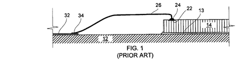
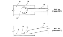
- ダイ上のダイパッドと、底部よりも頂部が小さい台形状の横断面を有するリードフィンガーとの間のワイヤボンド相互接続であって、前記リードフィンガーのボンドサイト上のサポート台座と、ダイパッド上のボールボンドと、前記サポート台座上のスティッチボンドとを備え、当該サポート台座は、当該リードフィンガーのみによって支持されるとともに、前記リードフィンガーの頂部にボンドされ、前記リードフィンガーの底部から離れている、ことを特徴とするワイヤボンド相互接続。
- ボンドサイトにおいてリードフィンガーは、サポート台座の径より狭くなっていることを特徴とする請求項1に記載のワイヤボンド相互接続。
- ボンドサイトにおいてリードフィンガーは、サポート台座の径より狭い平坦部を備えることを特徴とする請求項1に記載のワイヤボンド相互接続。
- ボンドサイトにおいてリードフィンガーの断面は、ベースと平坦部との間に傾斜した側面を備える略台形状の外観を有することを特徴とする請求項1に記載のワイヤボンド相互接続。
- ボンドサイトにおいてリードフィンガーは、ベースと、平坦部へ向けて集束する傾斜した側面を備え、サポート台座は、傾斜した側面の少なくとも1つについての少なくとも上部に一致するように変形することを特徴とする請求項1に記載のワイヤボンド相互接続。
- 複数のワイヤボンドによって基板にマウントされると共に電気的に接続されるダイを備える半導体パッケージであって、各前記ワイヤボンドは、前記ダイ上のパッドへボンドされるワイヤボールと、底部よりも頂部が小さい台形状の横断面を有するリードフィンガー上の、ボンドサイトの上のサポート台座へボンドされるスティッチとを備え、当該サポート台座は、当該リードフィンガーのみによって支持され、前記リードフィンガーの底部から離れていることを特徴とする半導体パッケージ。
- ボンドサイトにおいてリードフィンガーの幅は、サポート台座の径より小さいことを特徴とする請求項6に記載の半導体パッケージ。
- リードフィンガーボンドピッチは、100μmより小さいことを特徴とする請求項6に記載の半導体パッケージ。
- リードフィンガーボンドピッチは、ダイパッドピッチと同じであることを特徴とする請求項6に記載の半導体パッケージ。
- パッケージ基板は、2段の基板であり、各段は、複数のリードフィンガーを備え、第1段及び第2段のリードフィンガーは、前記2段の基板についてのリードフィンガーピッチが基板の各段についてのリードフィンガーピッチの半分となるように交互に配列されていることを特徴とする請求項6に記載の半導体パッケージ。
- 半導体ダイと基板との間のワイヤボンド相互接続を形成する方法であって、パターン付けされた配線を有する基板が底部よりも頂部が小さい台形状の横断面を有するリードフィンガーを備え、当該底部は当該基板の第1面上にあり、当該基板の第1面のダイマウント部に取付けられ、アクティブ面を基板から離れた方向へ向けられるダイを供給する工程と、リードフィンガーのボンドサイト上にサポート台座を形成する工程と、ダイパッド上に第1ボンドを形成する工程と、サポート台座上に第2ボンドを成形する工程とを備え、当該サポート台座は当該リードフィンガーによってのみ支持されるとともに、前記リードフィンガーの頂部にボンドされ、当該基板から離れている、ことを特徴とする方法。
- 第1ボンドは、ボールボンドを備えることを特徴とする請求項11に記載の方法。
- 第2ボンドは、スティッチボンドであることを特徴とする請求項11に記載の方法。
- サポート台座は、リードフィンガーへボンドされることを特徴とする請求項11に記載の方法。
- サポート台座は、スタッドバンピング操作にて形成されることを特徴とする請求項11に記載の方法。
Applications Claiming Priority (3)
| Application Number | Priority Date | Filing Date | Title |
|---|---|---|---|
| US62765004P | 2004-11-12 | 2004-11-12 | |
| US60/627,650 | 2004-11-12 | ||
| PCT/US2005/041116 WO2006053277A2 (en) | 2004-11-12 | 2005-11-14 | Wire bond interconnection |
Publications (3)
| Publication Number | Publication Date |
|---|---|
| JP2008520111A JP2008520111A (ja) | 2008-06-12 |
| JP2008520111A5 JP2008520111A5 (ja) | 2008-12-25 |
| JP4964780B2 true JP4964780B2 (ja) | 2012-07-04 |
Family
ID=36337287
Family Applications (1)
| Application Number | Title | Priority Date | Filing Date |
|---|---|---|---|
| JP2007541391A Expired - Lifetime JP4964780B2 (ja) | 2004-11-12 | 2005-11-14 | ワイヤボンド相互接続、半導体パッケージ、および、ワイヤボンド相互接続の形成方法 |
Country Status (5)
| Country | Link |
|---|---|
| US (4) | US7453156B2 (ja) |
| JP (1) | JP4964780B2 (ja) |
| KR (1) | KR101227228B1 (ja) |
| TW (1) | TWI368974B (ja) |
| WO (1) | WO2006053277A2 (ja) |
Families Citing this family (34)
| Publication number | Priority date | Publication date | Assignee | Title |
|---|---|---|---|---|
| US7868468B2 (en) * | 2004-11-12 | 2011-01-11 | Stats Chippac Ltd. | Wire bonding structure and method that eliminates special wire bondable finish and reduces bonding pitch on substrates |
| JP4964780B2 (ja) * | 2004-11-12 | 2012-07-04 | スタッツ・チップパック・インコーポレイテッド | ワイヤボンド相互接続、半導体パッケージ、および、ワイヤボンド相互接続の形成方法 |
| US8519517B2 (en) * | 2004-11-13 | 2013-08-27 | Stats Chippac Ltd. | Semiconductor system with fine pitch lead fingers and method of manufacturing thereof |
| US7731078B2 (en) * | 2004-11-13 | 2010-06-08 | Stats Chippac Ltd. | Semiconductor system with fine pitch lead fingers |
| EP3479844B1 (en) | 2005-04-15 | 2023-11-22 | MacroGenics, Inc. | Covalent diabodies and uses thereof |
| TW200642012A (en) * | 2005-05-17 | 2006-12-01 | Advanced Semiconductor Eng | Chip package and wire bonding process thereof |
| US20070018292A1 (en) * | 2005-07-22 | 2007-01-25 | Sehat Sutardja | Packaging for high speed integrated circuits |
| US20070026573A1 (en) * | 2005-07-28 | 2007-02-01 | Aminuddin Ismail | Method of making a stacked die package |
| US7863099B2 (en) * | 2007-06-27 | 2011-01-04 | Stats Chippac Ltd. | Integrated circuit package system with overhanging connection stack |
| SG148901A1 (en) | 2007-07-09 | 2009-01-29 | Micron Technology Inc | Packaged semiconductor assemblies and methods for manufacturing such assemblies |
| US7701049B2 (en) * | 2007-08-03 | 2010-04-20 | Stats Chippac Ltd. | Integrated circuit packaging system for fine pitch substrates |
| US20090243051A1 (en) * | 2008-03-28 | 2009-10-01 | Micron Technology, Inc. | Integrated conductive shield for microelectronic device assemblies and associated methods |
| US7897502B2 (en) | 2008-09-10 | 2011-03-01 | Stats Chippac, Ltd. | Method of forming vertically offset bond on trace interconnects on recessed and raised bond fingers |
| US7973394B2 (en) * | 2009-06-10 | 2011-07-05 | Blondwich Limited | Enhanced integrated circuit package |
| KR102057221B1 (ko) * | 2009-09-16 | 2019-12-18 | 가부시키가이샤 한도오따이 에네루기 켄큐쇼 | 반도체 장치 및 그 제조 방법 |
| US8304921B2 (en) * | 2009-11-13 | 2012-11-06 | Stats Chippac Ltd. | Integrated circuit packaging system with interconnect and method of manufacture thereof |
| US8039384B2 (en) | 2010-03-09 | 2011-10-18 | Stats Chippac, Ltd. | Semiconductor device and method of forming vertically offset bond on trace interconnects on different height traces |
| US8409978B2 (en) | 2010-06-24 | 2013-04-02 | Stats Chippac, Ltd. | Semiconductor device and method of forming vertically offset bond on trace interconnect structure on leadframe |
| US8609525B2 (en) * | 2011-03-21 | 2013-12-17 | Stats Chippac Ltd. | Integrated circuit packaging system with interconnects and method of manufacture thereof |
| JP5990897B2 (ja) | 2011-11-25 | 2016-09-14 | ソニー株式会社 | 電力制御装置、送電装置、および電力制御システム |
| US8643159B2 (en) | 2012-04-09 | 2014-02-04 | Freescale Semiconductor, Inc. | Lead frame with grooved lead finger |
| JP2013229368A (ja) * | 2012-04-24 | 2013-11-07 | Denso Corp | 電子装置およびその製造方法 |
| JP5894502B2 (ja) * | 2012-06-04 | 2016-03-30 | ローム株式会社 | ワイヤボンディング構造および半導体装置 |
| US9837188B2 (en) * | 2012-07-06 | 2017-12-05 | Nxp B.V. | Differential return loss supporting high speed bus interfaces |
| KR20150056531A (ko) * | 2012-09-24 | 2015-05-26 | 르네사스 일렉트로닉스 가부시키가이샤 | 반도체 장치의 제조 방법 및 반도체 장치 |
| US8680660B1 (en) | 2013-03-12 | 2014-03-25 | Freescale Semiconductor, Inc. | Brace for bond wire |
| US20140312474A1 (en) * | 2013-04-19 | 2014-10-23 | Texas Instruments Incorporated | Semiconductor package with wire bonding |
| KR101563911B1 (ko) | 2013-10-24 | 2015-10-28 | 앰코 테크놀로지 코리아 주식회사 | 반도체 패키지 |
| JP6279339B2 (ja) * | 2014-02-07 | 2018-02-14 | ルネサスエレクトロニクス株式会社 | 半導体装置の製造方法 |
| US9881870B2 (en) * | 2015-12-30 | 2018-01-30 | Taiwan Semiconductor Manufacturing Co., Ltd. | Semiconductor device and manufacturing method thereof |
| US10600756B1 (en) | 2017-02-15 | 2020-03-24 | United States Of America, As Represented By The Secretary Of The Navy | Wire bonding technique for integrated circuit board connections |
| LT3976597T (lt) | 2019-05-31 | 2024-10-10 | Janssen Pharmaceutica Nv | Nf-κb indukuojančios kinazės mažos molekulės inhibitoriai |
| KR20230173269A (ko) | 2022-06-16 | 2023-12-27 | 삼성전자주식회사 | 반도체 패키지 |
| GB2621374B (en) | 2022-08-10 | 2026-03-11 | Toshiba Kk | An electronic package and method of manufacturing an electronic package |
Family Cites Families (56)
| Publication number | Priority date | Publication date | Assignee | Title |
|---|---|---|---|---|
| JPS5933894A (ja) * | 1982-08-19 | 1984-02-23 | 電気化学工業株式会社 | 混成集積用回路基板の製造法 |
| US4742023A (en) * | 1986-08-28 | 1988-05-03 | Fujitsu Limited | Method for producing a semiconductor device |
| US5007576A (en) * | 1989-12-26 | 1991-04-16 | Hughes Aircraft Company | Testable ribbon bonding method and wedge bonding tool for microcircuit device fabrication |
| US5158647A (en) * | 1991-01-10 | 1992-10-27 | Raymond Hurley | Capacitor papers of flash-spun synthetic pulp fibers |
| JP2601666Y2 (ja) * | 1992-05-08 | 1999-11-29 | 株式会社村田製作所 | 積層型コイル |
| US5340772A (en) * | 1992-07-17 | 1994-08-23 | Lsi Logic Corporation | Method of increasing the layout efficiency of dies on a wafer and increasing the ratio of I/O area to active area per die |
| US5340770A (en) * | 1992-10-23 | 1994-08-23 | Ncr Corporation | Method of making a shallow junction by using first and second SOG layers |
| US5328079A (en) * | 1993-03-19 | 1994-07-12 | National Semiconductor Corporation | Method of and arrangement for bond wire connecting together certain integrated circuit components |
| US5561086A (en) * | 1993-06-18 | 1996-10-01 | Lsi Logic Corporation | Techniques for mounting semiconductor dies in die-receiving areas having support structure having notches |
| US5480834A (en) * | 1993-12-13 | 1996-01-02 | Micron Communications, Inc. | Process of manufacturing an electrical bonding interconnect having a metal bond pad portion and having a conductive epoxy portion comprising an oxide reducing agent |
| KR0130534B1 (ko) | 1994-07-12 | 1998-04-09 | 김광호 | 세탁기용 리니어 모터 |
| US5444303A (en) * | 1994-08-10 | 1995-08-22 | Motorola, Inc. | Wire bond pad arrangement having improved pad density |
| JPH08102517A (ja) * | 1994-09-30 | 1996-04-16 | Nec Corp | 半導体装置及びリードフレーム |
| US5465899A (en) * | 1994-10-14 | 1995-11-14 | Texas Instruments Incorporated | Method and apparatus for fine pitch wire bonding using a shaved capillary |
| US5994169A (en) * | 1994-10-27 | 1999-11-30 | Texas Instruments Incorporated | Lead frame for integrated circuits and process of packaging |
| US5842628A (en) * | 1995-04-10 | 1998-12-01 | Fujitsu Limited | Wire bonding method, semiconductor device, capillary for wire bonding and ball bump forming method |
| JPH0982742A (ja) * | 1995-09-11 | 1997-03-28 | Fujitsu Ltd | ワイヤボンディング方法 |
| US5686762A (en) * | 1995-12-21 | 1997-11-11 | Micron Technology, Inc. | Semiconductor device with improved bond pads |
| US5734559A (en) | 1996-03-29 | 1998-03-31 | Intel Corporation | Staggered bond finger design for fine pitch integrated circuit packages |
| US5904288A (en) * | 1996-04-08 | 1999-05-18 | Texas Instruments Incorporated | Wire bond clamping method |
| US6001671A (en) * | 1996-04-18 | 1999-12-14 | Tessera, Inc. | Methods for manufacturing a semiconductor package having a sacrificial layer |
| US5735030A (en) * | 1996-06-04 | 1998-04-07 | Texas Instruments Incorporated | Low loop wire bonding |
| US5976964A (en) * | 1997-04-22 | 1999-11-02 | Micron Technology, Inc. | Method of improving interconnect of semiconductor device by utilizing a flattened ball bond |
| JP3022819B2 (ja) * | 1997-08-27 | 2000-03-21 | 日本電気アイシーマイコンシステム株式会社 | 半導体集積回路装置 |
| EP0903780A3 (en) | 1997-09-19 | 1999-08-25 | Texas Instruments Incorporated | Method and apparatus for a wire bonded package for integrated circuits |
| US5960262A (en) * | 1997-09-26 | 1999-09-28 | Texas Instruments Incorporated | Stitch bond enhancement for hard-to-bond materials |
| US6008532A (en) | 1997-10-23 | 1999-12-28 | Lsi Logic Corporation | Integrated circuit package having bond fingers with alternate bonding areas |
| US6064113A (en) | 1998-01-13 | 2000-05-16 | Lsi Logic Corporation | Semiconductor device package including a substrate having bonding fingers within an electrically conductive ring surrounding a die area and a combined power and ground plane to stabilize signal path impedances |
| JPH11312749A (ja) * | 1998-02-25 | 1999-11-09 | Fujitsu Ltd | 半導体装置及びその製造方法及びリードフレームの製造方法 |
| US6158647A (en) | 1998-09-29 | 2000-12-12 | Micron Technology, Inc. | Concave face wire bond capillary |
| TW410446B (en) | 1999-01-21 | 2000-11-01 | Siliconware Precision Industries Co Ltd | BGA semiconductor package |
| US6462414B1 (en) * | 1999-03-05 | 2002-10-08 | Altera Corporation | Integrated circuit package utilizing a conductive structure for interlocking a conductive ball to a ball pad |
| US6329278B1 (en) * | 2000-01-03 | 2001-12-11 | Lsi Logic Corporation | Multiple row wire bonding with ball bonds of outer bond pads bonded on the leads |
| JP2001338955A (ja) * | 2000-05-29 | 2001-12-07 | Texas Instr Japan Ltd | 半導体装置及びその製造方法 |
| US6333562B1 (en) * | 2000-07-13 | 2001-12-25 | Advanced Semiconductor Engineering, Inc. | Multichip module having stacked chip arrangement |
| TW531867B (en) * | 2000-10-13 | 2003-05-11 | Texas Instruments Inc | Circuit structure integrating the power distribution functions of circuits and leadframes into the chip surface |
| US7135759B2 (en) * | 2000-10-27 | 2006-11-14 | Texas Instruments Incorporated | Individualized low parasitic power distribution lines deposited over active integrated circuits |
| US6597065B1 (en) * | 2000-11-03 | 2003-07-22 | Texas Instruments Incorporated | Thermally enhanced semiconductor chip having integrated bonds over active circuits |
| TW465064B (en) * | 2000-12-22 | 2001-11-21 | Advanced Semiconductor Eng | Bonding process and the structure thereof |
| JP2002368176A (ja) * | 2001-06-11 | 2002-12-20 | Rohm Co Ltd | 半導体電子部品のリードフレーム |
| TW495940B (en) | 2001-07-20 | 2002-07-21 | Via Tech Inc | Method for forming a grid array packaged integrated circuit |
| US6787926B2 (en) * | 2001-09-05 | 2004-09-07 | Taiwan Semiconductor Manufacturing Co., Ltd | Wire stitch bond on an integrated circuit bond pad and method of making the same |
| KR100396787B1 (ko) * | 2001-11-13 | 2003-09-02 | 엘지전자 주식회사 | 반도체 패키지용 인쇄회로기판의 와이어 본딩패드 형성방법 |
| US7190060B1 (en) * | 2002-01-09 | 2007-03-13 | Bridge Semiconductor Corporation | Three-dimensional stacked semiconductor package device with bent and flat leads and method of making same |
| JP3824545B2 (ja) * | 2002-02-07 | 2006-09-20 | 松下電器産業株式会社 | 配線基板、それを用いた半導体装置、それらの製造方法 |
| US7229906B2 (en) * | 2002-09-19 | 2007-06-12 | Kulicke And Soffa Industries, Inc. | Method and apparatus for forming bumps for semiconductor interconnections using a wire bonding machine |
| US6815836B2 (en) * | 2003-03-24 | 2004-11-09 | Texas Instruments Incorporated | Wire bonding for thin semiconductor package |
| US6927479B2 (en) * | 2003-06-25 | 2005-08-09 | St Assembly Test Services Ltd | Method of manufacturing a semiconductor package for a die larger than a die pad |
| US6956286B2 (en) * | 2003-08-05 | 2005-10-18 | International Business Machines Corporation | Integrated circuit package with overlapping bond fingers |
| US20050133928A1 (en) * | 2003-12-19 | 2005-06-23 | Howard Gregory E. | Wire loop grid array package |
| US7375978B2 (en) | 2003-12-23 | 2008-05-20 | Intel Corporation | Method and apparatus for trace shielding and routing on a substrate |
| KR100604840B1 (ko) * | 2004-03-11 | 2006-07-28 | 삼성전자주식회사 | 미세 피치 범프에의 리버스 와이어 본딩 방법 및 이에의한 와이어 본드 구조체 |
| TWI304238B (en) * | 2004-09-07 | 2008-12-11 | Advanced Semiconductor Eng | Wire-bonding method for connecting wire-bond pads and chip and the structure formed thereby |
| JP4964780B2 (ja) | 2004-11-12 | 2012-07-04 | スタッツ・チップパック・インコーポレイテッド | ワイヤボンド相互接続、半導体パッケージ、および、ワイヤボンド相互接続の形成方法 |
| US7731078B2 (en) * | 2004-11-13 | 2010-06-08 | Stats Chippac Ltd. | Semiconductor system with fine pitch lead fingers |
| US7358617B2 (en) * | 2004-11-29 | 2008-04-15 | Texas Instruments Incorporated | Bond pad for ball grid array package |
-
2005
- 2005-11-14 JP JP2007541391A patent/JP4964780B2/ja not_active Expired - Lifetime
- 2005-11-14 US US11/273,635 patent/US7453156B2/en active Active
- 2005-11-14 KR KR1020077010429A patent/KR101227228B1/ko not_active Expired - Lifetime
- 2005-11-14 TW TW094139959A patent/TWI368974B/zh not_active IP Right Cessation
- 2005-11-14 WO PCT/US2005/041116 patent/WO2006053277A2/en not_active Ceased
-
2008
- 2008-02-15 US US12/032,159 patent/US7745322B2/en not_active Expired - Lifetime
-
2010
- 2010-05-19 US US12/783,039 patent/US7986047B2/en not_active Expired - Lifetime
-
2011
- 2011-07-07 US US13/178,331 patent/US8129263B2/en not_active Expired - Lifetime
Also Published As
| Publication number | Publication date |
|---|---|
| US20080135997A1 (en) | 2008-06-12 |
| TW200623373A (en) | 2006-07-01 |
| JP2008520111A (ja) | 2008-06-12 |
| US20110266700A1 (en) | 2011-11-03 |
| US7986047B2 (en) | 2011-07-26 |
| TWI368974B (en) | 2012-07-21 |
| US20100225008A1 (en) | 2010-09-09 |
| US7745322B2 (en) | 2010-06-29 |
| US8129263B2 (en) | 2012-03-06 |
| KR101227228B1 (ko) | 2013-01-28 |
| US7453156B2 (en) | 2008-11-18 |
| KR20070084060A (ko) | 2007-08-24 |
| WO2006053277A3 (en) | 2007-06-21 |
| US20060113665A1 (en) | 2006-06-01 |
| WO2006053277A2 (en) | 2006-05-18 |
Similar Documents
| Publication | Publication Date | Title |
|---|---|---|
| JP4964780B2 (ja) | ワイヤボンド相互接続、半導体パッケージ、および、ワイヤボンド相互接続の形成方法 | |
| US10510659B2 (en) | Substrate-less stackable package with wire-bond interconnect | |
| US7176570B2 (en) | Method for forming bump, semiconductor element having bumps and method of manufacturing the same, semiconductor device and method of manufacturing the same, circuit board, and electronic equipment | |
| US8008785B2 (en) | Microelectronic assembly with joined bond elements having lowered inductance | |
| US9685365B2 (en) | Method of forming a wire bond having a free end | |
| US7064425B2 (en) | Semiconductor device circuit board, and electronic equipment | |
| JP5651608B2 (ja) | インピーダンス制御されたワイヤ・ボンド及び導電性基準部品を有するマイクロ電子アセンブリ | |
| US6921016B2 (en) | Semiconductor device and method of manufacturing the same, circuit board, and electronic equipment | |
| TW201431030A (zh) | 具有阻抗控制引線接合及參考引線接合之微電子總成 | |
| US8269356B2 (en) | Wire bonding structure and method that eliminates special wire bondable finish and reduces bonding pitch on substrates | |
| JPS61274333A (ja) | 半導体装置 | |
| US20110147928A1 (en) | Microelectronic assembly with bond elements having lowered inductance | |
| JPH08306724A (ja) | 半導体装置およびその製造方法ならびにその実装方法 | |
| JP2003234427A (ja) | 配線基板、それを用いた半導体装置、それらの製造方法 | |
| JP5048990B2 (ja) | 半導体装置及びその製造方法 | |
| JP2010056349A (ja) | 半導体素子、半導体素子製造装置用ツールおよび半導体素子の製造方法 |
Legal Events
| Date | Code | Title | Description |
|---|---|---|---|
| A521 | Request for written amendment filed |
Free format text: JAPANESE INTERMEDIATE CODE: A523 Effective date: 20081110 |
|
| A621 | Written request for application examination |
Free format text: JAPANESE INTERMEDIATE CODE: A621 Effective date: 20081110 |
|
| A977 | Report on retrieval |
Free format text: JAPANESE INTERMEDIATE CODE: A971007 Effective date: 20100804 |
|
| RD02 | Notification of acceptance of power of attorney |
Free format text: JAPANESE INTERMEDIATE CODE: A7422 Effective date: 20100810 |
|
| RD04 | Notification of resignation of power of attorney |
Free format text: JAPANESE INTERMEDIATE CODE: A7424 Effective date: 20100823 |
|
| A521 | Request for written amendment filed |
Free format text: JAPANESE INTERMEDIATE CODE: A821 Effective date: 20100810 |
|
| RD04 | Notification of resignation of power of attorney |
Free format text: JAPANESE INTERMEDIATE CODE: A7424 Effective date: 20100823 |
|
| A131 | Notification of reasons for refusal |
Free format text: JAPANESE INTERMEDIATE CODE: A131 Effective date: 20110215 |
|
| A521 | Request for written amendment filed |
Free format text: JAPANESE INTERMEDIATE CODE: A523 Effective date: 20110513 |
|
| A02 | Decision of refusal |
Free format text: JAPANESE INTERMEDIATE CODE: A02 Effective date: 20110621 |
|
| A521 | Request for written amendment filed |
Free format text: JAPANESE INTERMEDIATE CODE: A523 Effective date: 20111020 |
|
| A911 | Transfer to examiner for re-examination before appeal (zenchi) |
Free format text: JAPANESE INTERMEDIATE CODE: A911 Effective date: 20111031 |
|
| A131 | Notification of reasons for refusal |
Free format text: JAPANESE INTERMEDIATE CODE: A131 Effective date: 20111115 |
|
| A521 | Request for written amendment filed |
Free format text: JAPANESE INTERMEDIATE CODE: A523 Effective date: 20120213 |
|
| TRDD | Decision of grant or rejection written | ||
| A01 | Written decision to grant a patent or to grant a registration (utility model) |
Free format text: JAPANESE INTERMEDIATE CODE: A01 Effective date: 20120306 |
|
| A01 | Written decision to grant a patent or to grant a registration (utility model) |
Free format text: JAPANESE INTERMEDIATE CODE: A01 |
|
| A61 | First payment of annual fees (during grant procedure) |
Free format text: JAPANESE INTERMEDIATE CODE: A61 Effective date: 20120328 |
|
| R150 | Certificate of patent or registration of utility model |
Ref document number: 4964780 Country of ref document: JP Free format text: JAPANESE INTERMEDIATE CODE: R150 |
|
| FPAY | Renewal fee payment (event date is renewal date of database) |
Free format text: PAYMENT UNTIL: 20150406 Year of fee payment: 3 |
|
| R250 | Receipt of annual fees |
Free format text: JAPANESE INTERMEDIATE CODE: R250 |
|
| R250 | Receipt of annual fees |
Free format text: JAPANESE INTERMEDIATE CODE: R250 |
|
| R250 | Receipt of annual fees |
Free format text: JAPANESE INTERMEDIATE CODE: R250 |
|
| R250 | Receipt of annual fees |
Free format text: JAPANESE INTERMEDIATE CODE: R250 |
|
| R250 | Receipt of annual fees |
Free format text: JAPANESE INTERMEDIATE CODE: R250 |
|
| R250 | Receipt of annual fees |
Free format text: JAPANESE INTERMEDIATE CODE: R250 |
|
| R250 | Receipt of annual fees |
Free format text: JAPANESE INTERMEDIATE CODE: R250 |
|
| R250 | Receipt of annual fees |
Free format text: JAPANESE INTERMEDIATE CODE: R250 |
|
| R250 | Receipt of annual fees |
Free format text: JAPANESE INTERMEDIATE CODE: R250 |
|
| R250 | Receipt of annual fees |
Free format text: JAPANESE INTERMEDIATE CODE: R250 |
|
| R250 | Receipt of annual fees |
Free format text: JAPANESE INTERMEDIATE CODE: R250 |
|
| EXPY | Cancellation because of completion of term |