US5480834A - Process of manufacturing an electrical bonding interconnect having a metal bond pad portion and having a conductive epoxy portion comprising an oxide reducing agent - Google Patents
Process of manufacturing an electrical bonding interconnect having a metal bond pad portion and having a conductive epoxy portion comprising an oxide reducing agent Download PDFInfo
- Publication number
- US5480834A US5480834A US08/166,747 US16674793A US5480834A US 5480834 A US5480834 A US 5480834A US 16674793 A US16674793 A US 16674793A US 5480834 A US5480834 A US 5480834A
- Authority
- US
- United States
- Prior art keywords
- conductive
- epoxy
- metal
- contact area
- conductive epoxy
- Prior art date
- Legal status (The legal status is an assumption and is not a legal conclusion. Google has not performed a legal analysis and makes no representation as to the accuracy of the status listed.)
- Expired - Lifetime
Links
Images
Classifications
-
- H—ELECTRICITY
- H05—ELECTRIC TECHNIQUES NOT OTHERWISE PROVIDED FOR
- H05K—PRINTED CIRCUITS; CASINGS OR CONSTRUCTIONAL DETAILS OF ELECTRIC APPARATUS; MANUFACTURE OF ASSEMBLAGES OF ELECTRICAL COMPONENTS
- H05K3/00—Apparatus or processes for manufacturing printed circuits
- H05K3/30—Assembling printed circuits with electric components, e.g. with resistor
- H05K3/32—Assembling printed circuits with electric components, e.g. with resistor electrically connecting electric components or wires to printed circuits
- H05K3/321—Assembling printed circuits with electric components, e.g. with resistor electrically connecting electric components or wires to printed circuits by conductive adhesives
-
- H—ELECTRICITY
- H01—ELECTRIC ELEMENTS
- H01L—SEMICONDUCTOR DEVICES NOT COVERED BY CLASS H10
- H01L24/00—Arrangements for connecting or disconnecting semiconductor or solid-state bodies; Methods or apparatus related thereto
- H01L24/01—Means for bonding being attached to, or being formed on, the surface to be connected, e.g. chip-to-package, die-attach, "first-level" interconnects; Manufacturing methods related thereto
- H01L24/02—Bonding areas ; Manufacturing methods related thereto
- H01L24/04—Structure, shape, material or disposition of the bonding areas prior to the connecting process
- H01L24/05—Structure, shape, material or disposition of the bonding areas prior to the connecting process of an individual bonding area
-
- H—ELECTRICITY
- H01—ELECTRIC ELEMENTS
- H01L—SEMICONDUCTOR DEVICES NOT COVERED BY CLASS H10
- H01L24/00—Arrangements for connecting or disconnecting semiconductor or solid-state bodies; Methods or apparatus related thereto
- H01L24/01—Means for bonding being attached to, or being formed on, the surface to be connected, e.g. chip-to-package, die-attach, "first-level" interconnects; Manufacturing methods related thereto
- H01L24/10—Bump connectors ; Manufacturing methods related thereto
- H01L24/11—Manufacturing methods
-
- H—ELECTRICITY
- H01—ELECTRIC ELEMENTS
- H01L—SEMICONDUCTOR DEVICES NOT COVERED BY CLASS H10
- H01L24/00—Arrangements for connecting or disconnecting semiconductor or solid-state bodies; Methods or apparatus related thereto
- H01L24/01—Means for bonding being attached to, or being formed on, the surface to be connected, e.g. chip-to-package, die-attach, "first-level" interconnects; Manufacturing methods related thereto
- H01L24/10—Bump connectors ; Manufacturing methods related thereto
- H01L24/12—Structure, shape, material or disposition of the bump connectors prior to the connecting process
- H01L24/13—Structure, shape, material or disposition of the bump connectors prior to the connecting process of an individual bump connector
-
- H—ELECTRICITY
- H01—ELECTRIC ELEMENTS
- H01L—SEMICONDUCTOR DEVICES NOT COVERED BY CLASS H10
- H01L24/00—Arrangements for connecting or disconnecting semiconductor or solid-state bodies; Methods or apparatus related thereto
- H01L24/01—Means for bonding being attached to, or being formed on, the surface to be connected, e.g. chip-to-package, die-attach, "first-level" interconnects; Manufacturing methods related thereto
- H01L24/26—Layer connectors, e.g. plate connectors, solder or adhesive layers; Manufacturing methods related thereto
- H01L24/28—Structure, shape, material or disposition of the layer connectors prior to the connecting process
- H01L24/29—Structure, shape, material or disposition of the layer connectors prior to the connecting process of an individual layer connector
-
- H—ELECTRICITY
- H01—ELECTRIC ELEMENTS
- H01L—SEMICONDUCTOR DEVICES NOT COVERED BY CLASS H10
- H01L24/00—Arrangements for connecting or disconnecting semiconductor or solid-state bodies; Methods or apparatus related thereto
- H01L24/80—Methods for connecting semiconductor or other solid state bodies using means for bonding being attached to, or being formed on, the surface to be connected
- H01L24/81—Methods for connecting semiconductor or other solid state bodies using means for bonding being attached to, or being formed on, the surface to be connected using a bump connector
-
- H—ELECTRICITY
- H01—ELECTRIC ELEMENTS
- H01L—SEMICONDUCTOR DEVICES NOT COVERED BY CLASS H10
- H01L24/00—Arrangements for connecting or disconnecting semiconductor or solid-state bodies; Methods or apparatus related thereto
- H01L24/80—Methods for connecting semiconductor or other solid state bodies using means for bonding being attached to, or being formed on, the surface to be connected
- H01L24/83—Methods for connecting semiconductor or other solid state bodies using means for bonding being attached to, or being formed on, the surface to be connected using a layer connector
-
- H—ELECTRICITY
- H01—ELECTRIC ELEMENTS
- H01L—SEMICONDUCTOR DEVICES NOT COVERED BY CLASS H10
- H01L2224/00—Indexing scheme for arrangements for connecting or disconnecting semiconductor or solid-state bodies and methods related thereto as covered by H01L24/00
- H01L2224/01—Means for bonding being attached to, or being formed on, the surface to be connected, e.g. chip-to-package, die-attach, "first-level" interconnects; Manufacturing methods related thereto
- H01L2224/02—Bonding areas; Manufacturing methods related thereto
- H01L2224/04—Structure, shape, material or disposition of the bonding areas prior to the connecting process
- H01L2224/05—Structure, shape, material or disposition of the bonding areas prior to the connecting process of an individual bonding area
- H01L2224/05001—Internal layers
- H01L2224/05099—Material
- H01L2224/051—Material with a principal constituent of the material being a metal or a metalloid, e.g. boron [B], silicon [Si], germanium [Ge], arsenic [As], antimony [Sb], tellurium [Te] and polonium [Po], and alloys thereof
- H01L2224/05117—Material with a principal constituent of the material being a metal or a metalloid, e.g. boron [B], silicon [Si], germanium [Ge], arsenic [As], antimony [Sb], tellurium [Te] and polonium [Po], and alloys thereof the principal constituent melting at a temperature of greater than or equal to 400°C and less than 950°C
- H01L2224/05124—Aluminium [Al] as principal constituent
-
- H—ELECTRICITY
- H01—ELECTRIC ELEMENTS
- H01L—SEMICONDUCTOR DEVICES NOT COVERED BY CLASS H10
- H01L2224/00—Indexing scheme for arrangements for connecting or disconnecting semiconductor or solid-state bodies and methods related thereto as covered by H01L24/00
- H01L2224/01—Means for bonding being attached to, or being formed on, the surface to be connected, e.g. chip-to-package, die-attach, "first-level" interconnects; Manufacturing methods related thereto
- H01L2224/02—Bonding areas; Manufacturing methods related thereto
- H01L2224/04—Structure, shape, material or disposition of the bonding areas prior to the connecting process
- H01L2224/05—Structure, shape, material or disposition of the bonding areas prior to the connecting process of an individual bonding area
- H01L2224/0554—External layer
- H01L2224/05599—Material
- H01L2224/056—Material with a principal constituent of the material being a metal or a metalloid, e.g. boron [B], silicon [Si], germanium [Ge], arsenic [As], antimony [Sb], tellurium [Te] and polonium [Po], and alloys thereof
- H01L2224/05638—Material with a principal constituent of the material being a metal or a metalloid, e.g. boron [B], silicon [Si], germanium [Ge], arsenic [As], antimony [Sb], tellurium [Te] and polonium [Po], and alloys thereof the principal constituent melting at a temperature of greater than or equal to 950°C and less than 1550°C
- H01L2224/05647—Copper [Cu] as principal constituent
-
- H—ELECTRICITY
- H01—ELECTRIC ELEMENTS
- H01L—SEMICONDUCTOR DEVICES NOT COVERED BY CLASS H10
- H01L2224/00—Indexing scheme for arrangements for connecting or disconnecting semiconductor or solid-state bodies and methods related thereto as covered by H01L24/00
- H01L2224/01—Means for bonding being attached to, or being formed on, the surface to be connected, e.g. chip-to-package, die-attach, "first-level" interconnects; Manufacturing methods related thereto
- H01L2224/10—Bump connectors; Manufacturing methods related thereto
- H01L2224/12—Structure, shape, material or disposition of the bump connectors prior to the connecting process
- H01L2224/13—Structure, shape, material or disposition of the bump connectors prior to the connecting process of an individual bump connector
- H01L2224/13001—Core members of the bump connector
- H01L2224/13099—Material
- H01L2224/1319—Material with a principal constituent of the material being a polymer, e.g. polyester, phenolic based polymer, epoxy
-
- H—ELECTRICITY
- H01—ELECTRIC ELEMENTS
- H01L—SEMICONDUCTOR DEVICES NOT COVERED BY CLASS H10
- H01L2224/00—Indexing scheme for arrangements for connecting or disconnecting semiconductor or solid-state bodies and methods related thereto as covered by H01L24/00
- H01L2224/01—Means for bonding being attached to, or being formed on, the surface to be connected, e.g. chip-to-package, die-attach, "first-level" interconnects; Manufacturing methods related thereto
- H01L2224/10—Bump connectors; Manufacturing methods related thereto
- H01L2224/15—Structure, shape, material or disposition of the bump connectors after the connecting process
- H01L2224/16—Structure, shape, material or disposition of the bump connectors after the connecting process of an individual bump connector
-
- H—ELECTRICITY
- H01—ELECTRIC ELEMENTS
- H01L—SEMICONDUCTOR DEVICES NOT COVERED BY CLASS H10
- H01L2224/00—Indexing scheme for arrangements for connecting or disconnecting semiconductor or solid-state bodies and methods related thereto as covered by H01L24/00
- H01L2224/01—Means for bonding being attached to, or being formed on, the surface to be connected, e.g. chip-to-package, die-attach, "first-level" interconnects; Manufacturing methods related thereto
- H01L2224/26—Layer connectors, e.g. plate connectors, solder or adhesive layers; Manufacturing methods related thereto
- H01L2224/28—Structure, shape, material or disposition of the layer connectors prior to the connecting process
- H01L2224/29—Structure, shape, material or disposition of the layer connectors prior to the connecting process of an individual layer connector
- H01L2224/29001—Core members of the layer connector
- H01L2224/29099—Material
- H01L2224/291—Material with a principal constituent of the material being a metal or a metalloid, e.g. boron [B], silicon [Si], germanium [Ge], arsenic [As], antimony [Sb], tellurium [Te] and polonium [Po], and alloys thereof
- H01L2224/29101—Material with a principal constituent of the material being a metal or a metalloid, e.g. boron [B], silicon [Si], germanium [Ge], arsenic [As], antimony [Sb], tellurium [Te] and polonium [Po], and alloys thereof the principal constituent melting at a temperature of less than 400°C
-
- H—ELECTRICITY
- H01—ELECTRIC ELEMENTS
- H01L—SEMICONDUCTOR DEVICES NOT COVERED BY CLASS H10
- H01L2224/00—Indexing scheme for arrangements for connecting or disconnecting semiconductor or solid-state bodies and methods related thereto as covered by H01L24/00
- H01L2224/01—Means for bonding being attached to, or being formed on, the surface to be connected, e.g. chip-to-package, die-attach, "first-level" interconnects; Manufacturing methods related thereto
- H01L2224/26—Layer connectors, e.g. plate connectors, solder or adhesive layers; Manufacturing methods related thereto
- H01L2224/28—Structure, shape, material or disposition of the layer connectors prior to the connecting process
- H01L2224/29—Structure, shape, material or disposition of the layer connectors prior to the connecting process of an individual layer connector
- H01L2224/29001—Core members of the layer connector
- H01L2224/29099—Material
- H01L2224/2919—Material with a principal constituent of the material being a polymer, e.g. polyester, phenolic based polymer, epoxy
-
- H—ELECTRICITY
- H01—ELECTRIC ELEMENTS
- H01L—SEMICONDUCTOR DEVICES NOT COVERED BY CLASS H10
- H01L2224/00—Indexing scheme for arrangements for connecting or disconnecting semiconductor or solid-state bodies and methods related thereto as covered by H01L24/00
- H01L2224/01—Means for bonding being attached to, or being formed on, the surface to be connected, e.g. chip-to-package, die-attach, "first-level" interconnects; Manufacturing methods related thereto
- H01L2224/42—Wire connectors; Manufacturing methods related thereto
- H01L2224/47—Structure, shape, material or disposition of the wire connectors after the connecting process
- H01L2224/48—Structure, shape, material or disposition of the wire connectors after the connecting process of an individual wire connector
- H01L2224/484—Connecting portions
- H01L2224/48463—Connecting portions the connecting portion on the bonding area of the semiconductor or solid-state body being a ball bond
-
- H—ELECTRICITY
- H01—ELECTRIC ELEMENTS
- H01L—SEMICONDUCTOR DEVICES NOT COVERED BY CLASS H10
- H01L2224/00—Indexing scheme for arrangements for connecting or disconnecting semiconductor or solid-state bodies and methods related thereto as covered by H01L24/00
- H01L2224/80—Methods for connecting semiconductor or other solid state bodies using means for bonding being attached to, or being formed on, the surface to be connected
- H01L2224/81—Methods for connecting semiconductor or other solid state bodies using means for bonding being attached to, or being formed on, the surface to be connected using a bump connector
- H01L2224/818—Bonding techniques
- H01L2224/81801—Soldering or alloying
-
- H—ELECTRICITY
- H01—ELECTRIC ELEMENTS
- H01L—SEMICONDUCTOR DEVICES NOT COVERED BY CLASS H10
- H01L2224/00—Indexing scheme for arrangements for connecting or disconnecting semiconductor or solid-state bodies and methods related thereto as covered by H01L24/00
- H01L2224/80—Methods for connecting semiconductor or other solid state bodies using means for bonding being attached to, or being formed on, the surface to be connected
- H01L2224/83—Methods for connecting semiconductor or other solid state bodies using means for bonding being attached to, or being formed on, the surface to be connected using a layer connector
- H01L2224/8319—Arrangement of the layer connectors prior to mounting
-
- H—ELECTRICITY
- H01—ELECTRIC ELEMENTS
- H01L—SEMICONDUCTOR DEVICES NOT COVERED BY CLASS H10
- H01L2224/00—Indexing scheme for arrangements for connecting or disconnecting semiconductor or solid-state bodies and methods related thereto as covered by H01L24/00
- H01L2224/80—Methods for connecting semiconductor or other solid state bodies using means for bonding being attached to, or being formed on, the surface to be connected
- H01L2224/83—Methods for connecting semiconductor or other solid state bodies using means for bonding being attached to, or being formed on, the surface to be connected using a layer connector
- H01L2224/838—Bonding techniques
-
- H—ELECTRICITY
- H01—ELECTRIC ELEMENTS
- H01L—SEMICONDUCTOR DEVICES NOT COVERED BY CLASS H10
- H01L24/00—Arrangements for connecting or disconnecting semiconductor or solid-state bodies; Methods or apparatus related thereto
- H01L24/01—Means for bonding being attached to, or being formed on, the surface to be connected, e.g. chip-to-package, die-attach, "first-level" interconnects; Manufacturing methods related thereto
- H01L24/10—Bump connectors ; Manufacturing methods related thereto
- H01L24/15—Structure, shape, material or disposition of the bump connectors after the connecting process
- H01L24/16—Structure, shape, material or disposition of the bump connectors after the connecting process of an individual bump connector
-
- H—ELECTRICITY
- H01—ELECTRIC ELEMENTS
- H01L—SEMICONDUCTOR DEVICES NOT COVERED BY CLASS H10
- H01L2924/00—Indexing scheme for arrangements or methods for connecting or disconnecting semiconductor or solid-state bodies as covered by H01L24/00
- H01L2924/01—Chemical elements
- H01L2924/01005—Boron [B]
-
- H—ELECTRICITY
- H01—ELECTRIC ELEMENTS
- H01L—SEMICONDUCTOR DEVICES NOT COVERED BY CLASS H10
- H01L2924/00—Indexing scheme for arrangements or methods for connecting or disconnecting semiconductor or solid-state bodies as covered by H01L24/00
- H01L2924/01—Chemical elements
- H01L2924/01006—Carbon [C]
-
- H—ELECTRICITY
- H01—ELECTRIC ELEMENTS
- H01L—SEMICONDUCTOR DEVICES NOT COVERED BY CLASS H10
- H01L2924/00—Indexing scheme for arrangements or methods for connecting or disconnecting semiconductor or solid-state bodies as covered by H01L24/00
- H01L2924/01—Chemical elements
- H01L2924/01013—Aluminum [Al]
-
- H—ELECTRICITY
- H01—ELECTRIC ELEMENTS
- H01L—SEMICONDUCTOR DEVICES NOT COVERED BY CLASS H10
- H01L2924/00—Indexing scheme for arrangements or methods for connecting or disconnecting semiconductor or solid-state bodies as covered by H01L24/00
- H01L2924/01—Chemical elements
- H01L2924/01029—Copper [Cu]
-
- H—ELECTRICITY
- H01—ELECTRIC ELEMENTS
- H01L—SEMICONDUCTOR DEVICES NOT COVERED BY CLASS H10
- H01L2924/00—Indexing scheme for arrangements or methods for connecting or disconnecting semiconductor or solid-state bodies as covered by H01L24/00
- H01L2924/01—Chemical elements
- H01L2924/01047—Silver [Ag]
-
- H—ELECTRICITY
- H01—ELECTRIC ELEMENTS
- H01L—SEMICONDUCTOR DEVICES NOT COVERED BY CLASS H10
- H01L2924/00—Indexing scheme for arrangements or methods for connecting or disconnecting semiconductor or solid-state bodies as covered by H01L24/00
- H01L2924/01—Chemical elements
- H01L2924/01078—Platinum [Pt]
-
- H—ELECTRICITY
- H01—ELECTRIC ELEMENTS
- H01L—SEMICONDUCTOR DEVICES NOT COVERED BY CLASS H10
- H01L2924/00—Indexing scheme for arrangements or methods for connecting or disconnecting semiconductor or solid-state bodies as covered by H01L24/00
- H01L2924/01—Chemical elements
- H01L2924/01079—Gold [Au]
-
- H—ELECTRICITY
- H01—ELECTRIC ELEMENTS
- H01L—SEMICONDUCTOR DEVICES NOT COVERED BY CLASS H10
- H01L2924/00—Indexing scheme for arrangements or methods for connecting or disconnecting semiconductor or solid-state bodies as covered by H01L24/00
- H01L2924/013—Alloys
- H01L2924/014—Solder alloys
-
- H—ELECTRICITY
- H01—ELECTRIC ELEMENTS
- H01L—SEMICONDUCTOR DEVICES NOT COVERED BY CLASS H10
- H01L2924/00—Indexing scheme for arrangements or methods for connecting or disconnecting semiconductor or solid-state bodies as covered by H01L24/00
- H01L2924/06—Polymers
- H01L2924/0665—Epoxy resin
-
- H—ELECTRICITY
- H01—ELECTRIC ELEMENTS
- H01L—SEMICONDUCTOR DEVICES NOT COVERED BY CLASS H10
- H01L2924/00—Indexing scheme for arrangements or methods for connecting or disconnecting semiconductor or solid-state bodies as covered by H01L24/00
- H01L2924/06—Polymers
- H01L2924/078—Adhesive characteristics other than chemical
- H01L2924/0781—Adhesive characteristics other than chemical being an ohmic electrical conductor
-
- H—ELECTRICITY
- H05—ELECTRIC TECHNIQUES NOT OTHERWISE PROVIDED FOR
- H05K—PRINTED CIRCUITS; CASINGS OR CONSTRUCTIONAL DETAILS OF ELECTRIC APPARATUS; MANUFACTURE OF ASSEMBLAGES OF ELECTRICAL COMPONENTS
- H05K2201/00—Indexing scheme relating to printed circuits covered by H05K1/00
- H05K2201/10—Details of components or other objects attached to or integrated in a printed circuit board
- H05K2201/10613—Details of electrical connections of non-printed components, e.g. special leads
- H05K2201/10621—Components characterised by their electrical contacts
- H05K2201/10674—Flip chip
-
- H—ELECTRICITY
- H05—ELECTRIC TECHNIQUES NOT OTHERWISE PROVIDED FOR
- H05K—PRINTED CIRCUITS; CASINGS OR CONSTRUCTIONAL DETAILS OF ELECTRIC APPARATUS; MANUFACTURE OF ASSEMBLAGES OF ELECTRICAL COMPONENTS
- H05K2201/00—Indexing scheme relating to printed circuits covered by H05K1/00
- H05K2201/10—Details of components or other objects attached to or integrated in a printed circuit board
- H05K2201/10613—Details of electrical connections of non-printed components, e.g. special leads
- H05K2201/10954—Other details of electrical connections
- H05K2201/10984—Component carrying a connection agent, e.g. solder, adhesive
Definitions
- the invention relates to semiconductor flip chip technology and more particularly to conductive epoxy attachment of a die pad to a supporting substrate.
- Flip chip interconnections made to connect a semiconductor die pad circuit to a semiconductor supporting substrate have historically been made with exotic plating methods and reflow solder attachment. More recently electrically conductive epoxy has been used to make the flip chip interconnections. These conductive epoxy interconnects have typically been plagued with high contact resistance. For example, when used to contact an aluminum bond pad, which is the semiconductor industry standard, a tenacious nonconductive oxide coated surface forms in a short amount of time, even at room temperature. Because of the nonconductive oxides present, electrically conductive epoxies on otherwise bare aluminum form an interconnect having an extremely high contact resistance. The resistance typically ranges from hundreds of ohms to millions of ohms.
- a more noble metal such as gold
- gold has been used to provide a very inert, oxide free surface over which the conductive epoxy may be applied.
- Gold precludes the formation of nonconductive metal oxides at the surface of the contact.
- gold, plated on an existing contact has a direct low contact resistance when it is bonded with a conductive epoxy.
- the gold plating of a semiconductor die pad is an elaborate process that can be very difficult, expensive and time consuming. It is very difficult because the process is typically not an electroless deposition process and therefore requires the substrates to be electrically connected to a power supply.
- the oxide formed during the epoxy application is mechanically removed, typically with abrasive action.
- the base metal is subjected to a chemical pre-treatment to prohibit oxide formation.
- the invention is a bonding interconnect comprising a bond pad portion and a conductive epoxy portion.
- the conductive epoxy portion comprises an oxide reducing agent which reduces oxides formed on the bond pad.
- the conductive epoxy is cured to bond the epoxy to the plated portion.
- the bonding interconnect of the invention has a low contact resistance and creates a good electrical interconnect to bond a die pad to a supporting substrate.
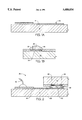
- FIG. 1A is a supporting substrate having a circuit trace.
- Figure 1B depicts a die pad having a copper plated bond pad bonded to conductive epoxy.
- FIG. 2 depicts a memory module comprising the supporting substrate and die pad of FIG. 1.
- the invention is an inexpensive low contact resistance electrical bonding interconnect and the method of forming the bonding interconnect.
- the bonding interconnect comprises a metal bond pad portion and a conductive epoxy portion.
- the conductive epoxy portion comprises a metal oxide reducing agent for reducing oxides formed on the metal bond pad.
- FIG. 1A depicts a supporting substrate 5, and FIG. 1B depicts a die pad 10.
- the die pad 10 typically consists of circuitry fabricated on a semiconductor substrate.
- the supporting substrate 5 is fabricated to have a circuit trace 14.
- the circuit trace 14 may be fabricated using any circuit trace technology including, but not limited to copper, aluminum, printed polymer thick film (copper, silver, or carbon) technologies.
- a portion of the circuit trace 14 is an electrical contact area 15.
- the die pad 10 is fabricated to have an electrical contact area 20.
- the contact area 20 is also referred to as a bond pad. Because of practical manufacturing considerations the contact area 20 of the present embodiment is aluminum, although other conductive metals may be used.
- the exposed aluminum on the die pad 10 is electroless copper plated to form a copper layer 26.
- Electroless copper plating is well known to those skilled in the art. Although copper is the metal of choice in the preferred embodiment other conductive metals may be used in place of copper.
- a conductive epoxy 30 is formulated to have a copper oxide reducing agent and is applied to the copper layer 26 overlying contact area 20.
- the copper layer 26 forms an interface layer on the aluminum contact area 20 in order to provide a desired surface for the conductive epoxy 30.
- the copper layer 26 and the contact area 20 form the metal bond pad portion and the conductive epoxy 30 forms the conductive epoxy portion of the electrical bonding interconnect 31.
- the epoxy is cured to harden it and increase the adhesive bond between the conductive epoxy 30 and the copper layer 26, thereby completing the fabrication of the electrical bonding interconnect.
- a wide variety of metal oxide reducing agents are compatible with the epoxy used in the epoxy industry, including, but not limited to, alkoxylated polyalkyl amine and ethylene diamine.
- alkoxylated polyalkyl amine and ethylene diamine One example of an epoxy containing a curing agent which is also a copper oxide reducing agent that was found to have a very low contact resistance is manufactured by Tra-Con, Incorporated located at 55 North Street, Medford, Mass., 02155. The specific material was Tra-Con hardener "Tra-Duct 2922 Hardener", containing in significant part polyalkyl amine and ethylene diamine.
- Other epoxies contain curing agents which are not oxide reducing agents, and accordingly were ineffective in reducing copper oxide.
- An ineffective material, having no alkoxylated polyalkyl amine or ethylene diamine is "Ablebond 8380" manufactured by Ablestik located at 20021 Suzana Road, Collinso Dominguez, Calif.
- the oxide reducing agent in the conductive epoxy is selected to reduce the oxides formed before and/or during the process of the invention.
- the conductive epoxy portion 30 is applied to the die pad by placing a screen over the die pad 10 and over the copper layer 26. Correct positioning of the screen aligns a screen opening with the contact area 20. The screen opening is filled with the conductive epoxy and excess epoxy is removed. The screen is then removed and the conductive epoxy portion 30 overlying the contact area 15 remains.
- the process can be continued to form a memory module 35 shown in FIG. 2.
- a small amount of liquid conductive epoxy is applied to the contact area 15 of the substrate 5.
- the die pad 10 is positioned over the supporting substrate 5 such that the contact areas 15 and 20 are aligned.
- the cured epoxy functions as a standoff between the die pad 10 and substrate 5.
- the wet epoxy is then cured, bonding the die pad 10 and the substrate 5 together.
- a wire bond 40 may be used to electrically connect the supporting substrate to an external electrical connection.
- the bonding pad of the described embodiment comprises a first conductive layer and a plated layer the invention is equally applicable in the case where the conductive epoxy is applied to a conductive layer which is not plated.
Landscapes
- Engineering & Computer Science (AREA)
- Microelectronics & Electronic Packaging (AREA)
- Computer Hardware Design (AREA)
- Power Engineering (AREA)
- Manufacturing & Machinery (AREA)
- Wire Bonding (AREA)
Abstract
Description
Claims (3)
Priority Applications (4)
| Application Number | Priority Date | Filing Date | Title |
|---|---|---|---|
| US08/166,747 US5480834A (en) | 1993-12-13 | 1993-12-13 | Process of manufacturing an electrical bonding interconnect having a metal bond pad portion and having a conductive epoxy portion comprising an oxide reducing agent |
| US08/553,762 US5663598A (en) | 1993-12-13 | 1995-10-23 | Electrical circuit bonding interconnect component and flip chip interconnect bond |
| US08/853,852 US5804876A (en) | 1993-12-13 | 1997-05-09 | Electronic circuit bonding interconnect component and flip chip interconnect bond |
| US09/111,921 US6114239A (en) | 1993-12-13 | 1998-07-08 | Electronic circuit bonding interconnect component and flip chip interconnect bond |
Applications Claiming Priority (1)
| Application Number | Priority Date | Filing Date | Title |
|---|---|---|---|
| US08/166,747 US5480834A (en) | 1993-12-13 | 1993-12-13 | Process of manufacturing an electrical bonding interconnect having a metal bond pad portion and having a conductive epoxy portion comprising an oxide reducing agent |
Related Child Applications (1)
| Application Number | Title | Priority Date | Filing Date |
|---|---|---|---|
| US08/553,762 Division US5663598A (en) | 1993-12-13 | 1995-10-23 | Electrical circuit bonding interconnect component and flip chip interconnect bond |
Publications (1)
| Publication Number | Publication Date |
|---|---|
| US5480834A true US5480834A (en) | 1996-01-02 |
Family
ID=22604547
Family Applications (4)
| Application Number | Title | Priority Date | Filing Date |
|---|---|---|---|
| US08/166,747 Expired - Lifetime US5480834A (en) | 1993-12-13 | 1993-12-13 | Process of manufacturing an electrical bonding interconnect having a metal bond pad portion and having a conductive epoxy portion comprising an oxide reducing agent |
| US08/553,762 Expired - Lifetime US5663598A (en) | 1993-12-13 | 1995-10-23 | Electrical circuit bonding interconnect component and flip chip interconnect bond |
| US08/853,852 Expired - Lifetime US5804876A (en) | 1993-12-13 | 1997-05-09 | Electronic circuit bonding interconnect component and flip chip interconnect bond |
| US09/111,921 Expired - Lifetime US6114239A (en) | 1993-12-13 | 1998-07-08 | Electronic circuit bonding interconnect component and flip chip interconnect bond |
Family Applications After (3)
| Application Number | Title | Priority Date | Filing Date |
|---|---|---|---|
| US08/553,762 Expired - Lifetime US5663598A (en) | 1993-12-13 | 1995-10-23 | Electrical circuit bonding interconnect component and flip chip interconnect bond |
| US08/853,852 Expired - Lifetime US5804876A (en) | 1993-12-13 | 1997-05-09 | Electronic circuit bonding interconnect component and flip chip interconnect bond |
| US09/111,921 Expired - Lifetime US6114239A (en) | 1993-12-13 | 1998-07-08 | Electronic circuit bonding interconnect component and flip chip interconnect bond |
Country Status (1)
| Country | Link |
|---|---|
| US (4) | US5480834A (en) |
Cited By (21)
| Publication number | Priority date | Publication date | Assignee | Title |
|---|---|---|---|---|
| US5720859A (en) * | 1996-06-03 | 1998-02-24 | Raychem Corporation | Method of forming an electrode on a substrate |
| US5898223A (en) * | 1997-10-08 | 1999-04-27 | Lucent Technologies Inc. | Chip-on-chip IC packages |
| US5937277A (en) * | 1994-01-31 | 1999-08-10 | Fujitsu Limited | Semiconductor device with reliable electrodes of projecting shape and method of forming same |
| US6051879A (en) * | 1997-12-16 | 2000-04-18 | Micron Technology, Inc. | Electrical interconnection for attachment to a substrate |
| US6088215A (en) * | 1997-11-03 | 2000-07-11 | Motorola, Inc. | Capacitor and method of manufacture |
| US6114239A (en) * | 1993-12-13 | 2000-09-05 | Micron Communications, Inc. | Electronic circuit bonding interconnect component and flip chip interconnect bond |
| US6204074B1 (en) * | 1995-01-09 | 2001-03-20 | International Business Machines Corporation | Chip design process for wire bond and flip-chip package |
| US6229216B1 (en) * | 1999-01-11 | 2001-05-08 | Intel Corporation | Silicon interposer and multi-chip-module (MCM) with through substrate vias |
| US20010002826A1 (en) * | 1997-05-01 | 2001-06-07 | Mark E. Tuttle | Embedded circuits |
| US20040085190A1 (en) * | 1996-07-30 | 2004-05-06 | Tuttle Mark E. | Radio frequency data communications device with adjustable receiver sensitivity and method |
| US6890065B1 (en) | 2000-07-25 | 2005-05-10 | Lexmark International, Inc. | Heater chip for an inkjet printhead |
| US20050242964A1 (en) * | 1992-08-12 | 2005-11-03 | Tuttle John R | Miniature radio frequency transceiver |
| US20060082445A1 (en) * | 1996-05-13 | 2006-04-20 | O'toole James E | Radio frequency data communications device |
| US20060097849A1 (en) * | 1997-08-18 | 2006-05-11 | Dando Ross S | Wireless communication devices and methods of forming and operating the same |
| US7064447B2 (en) | 2001-08-10 | 2006-06-20 | Micron Technology, Inc. | Bond pad structure comprising multiple bond pads with metal overlap |
| US20070124897A1 (en) * | 2005-12-01 | 2007-06-07 | Wilson Eric J | Clamp for circular objects |
| US20070222611A1 (en) * | 2000-04-26 | 2007-09-27 | Micron Technology, Inc. | Automated antenna trim for transmitting and receiving semiconductor devices |
| US20080291027A1 (en) * | 1998-02-12 | 2008-11-27 | Lake Rickie C | Thin Profile Battery Bonding Method, Method Of Conductively Interconnecting Electronic Components, Battery Powerable Apparatus, Radio Frequency Communication Device, And Electric Circuit |
| US7839285B2 (en) | 1997-08-20 | 2010-11-23 | Round Rock Resarch, LLC | Electronic communication devices, methods of forming electrical communication devices, and communications methods |
| USRE42773E1 (en) | 1992-06-17 | 2011-10-04 | Round Rock Research, Llc | Method of manufacturing an enclosed transceiver |
| CN113192971A (en) * | 2021-04-01 | 2021-07-30 | 深圳市华星光电半导体显示技术有限公司 | Driving back plate and preparation method of micro light-emitting diode back plate |
Families Citing this family (77)
| Publication number | Priority date | Publication date | Assignee | Title |
|---|---|---|---|---|
| JP3561084B2 (en) * | 1995-07-24 | 2004-09-02 | シャープ株式会社 | Photodetector with built-in circuit, electronic component, optical pickup device, and method of manufacturing photodetector with built-in circuit |
| JPH1126631A (en) * | 1997-07-02 | 1999-01-29 | Matsushita Electric Ind Co Ltd | Semiconductor device and manufacture thereof |
| TW392325B (en) * | 1998-05-01 | 2000-06-01 | United Microelectronics Corp | Structure of metallization and process thereof |
| US6406939B1 (en) | 1998-05-02 | 2002-06-18 | Charles W. C. Lin | Flip chip assembly with via interconnection |
| SG75841A1 (en) | 1998-05-02 | 2000-10-24 | Eriston Invest Pte Ltd | Flip chip assembly with via interconnection |
| US5897341A (en) * | 1998-07-02 | 1999-04-27 | Fujitsu Limited | Diffusion bonded interconnect |
| US6452271B2 (en) | 1998-07-31 | 2002-09-17 | Micron Technology, Inc. | Interconnect component for a semiconductor die including a ruthenium layer and a method for its fabrication |
| US6179659B1 (en) | 1998-08-11 | 2001-01-30 | Micron Technology, Inc. | Electrical contact device and associated method of manufacture |
| US6169331B1 (en) | 1998-08-28 | 2001-01-02 | Micron Technology, Inc. | Apparatus for electrically coupling bond pads of a microelectronic device |
| TW396462B (en) | 1998-12-17 | 2000-07-01 | Eriston Technologies Pte Ltd | Bumpless flip chip assembly with solder via |
| SG78324A1 (en) | 1998-12-17 | 2001-02-20 | Eriston Technologies Pte Ltd | Bumpless flip chip assembly with strips-in-via and plating |
| TW444236B (en) | 1998-12-17 | 2001-07-01 | Charles Wen Chyang Lin | Bumpless flip chip assembly with strips and via-fill |
| US6303500B1 (en) * | 1999-02-24 | 2001-10-16 | Micron Technology, Inc. | Method and apparatus for electroless plating a contact pad |
| US6403457B2 (en) * | 1999-08-25 | 2002-06-11 | Micron Technology, Inc. | Selectively coating bond pads |
| US6570251B1 (en) * | 1999-09-02 | 2003-05-27 | Micron Technology, Inc. | Under bump metalization pad and solder bump connections |
| US6306751B1 (en) * | 1999-09-27 | 2001-10-23 | Lsi Logic Corporation | Apparatus and method for improving ball joints in semiconductor packages |
| US6821888B2 (en) * | 2000-07-07 | 2004-11-23 | Chartered Semiconductor Manufacturing Ltd. | Method of copper/copper surface bonding using a conducting polymer for application in IC chip bonding |
| US6340608B1 (en) | 2000-07-07 | 2002-01-22 | Chartered Semiconductor Manufacturing Ltd. | Method of fabricating copper metal bumps for flip-chip or chip-on-board IC bonding on terminating copper pads |
| US6551861B1 (en) | 2000-08-22 | 2003-04-22 | Charles W. C. Lin | Method of making a semiconductor chip assembly by joining the chip to a support circuit with an adhesive |
| US6402970B1 (en) | 2000-08-22 | 2002-06-11 | Charles W. C. Lin | Method of making a support circuit for a semiconductor chip assembly |
| US6350633B1 (en) | 2000-08-22 | 2002-02-26 | Charles W. C. Lin | Semiconductor chip assembly with simultaneously electroplated contact terminal and connection joint |
| US6660626B1 (en) | 2000-08-22 | 2003-12-09 | Charles W. C. Lin | Semiconductor chip assembly with simultaneously electrolessly plated contact terminal and connection joint |
| US6403460B1 (en) | 2000-08-22 | 2002-06-11 | Charles W. C. Lin | Method of making a semiconductor chip assembly |
| US6562657B1 (en) | 2000-08-22 | 2003-05-13 | Charles W. C. Lin | Semiconductor chip assembly with simultaneously electrolessly plated contact terminal and connection joint |
| US6562709B1 (en) | 2000-08-22 | 2003-05-13 | Charles W. C. Lin | Semiconductor chip assembly with simultaneously electroplated contact terminal and connection joint |
| US6436734B1 (en) | 2000-08-22 | 2002-08-20 | Charles W. C. Lin | Method of making a support circuit for a semiconductor chip assembly |
| US6511865B1 (en) | 2000-09-20 | 2003-01-28 | Charles W. C. Lin | Method for forming a ball bond connection joint on a conductive trace and conductive pad in a semiconductor chip assembly |
| US6350386B1 (en) | 2000-09-20 | 2002-02-26 | Charles W. C. Lin | Method of making a support circuit with a tapered through-hole for a semiconductor chip assembly |
| US6350632B1 (en) | 2000-09-20 | 2002-02-26 | Charles W. C. Lin | Semiconductor chip assembly with ball bond connection joint |
| US6544813B1 (en) | 2000-10-02 | 2003-04-08 | Charles W. C. Lin | Method of making a semiconductor chip assembly with a conductive trace subtractively formed before and after chip attachment |
| US6448108B1 (en) | 2000-10-02 | 2002-09-10 | Charles W. C. Lin | Method of making a semiconductor chip assembly with a conductive trace subtractively formed before and after chip attachment |
| US7129113B1 (en) | 2000-10-13 | 2006-10-31 | Bridge Semiconductor Corporation | Method of making a three-dimensional stacked semiconductor package with a metal pillar in an encapsulant aperture |
| US6740576B1 (en) | 2000-10-13 | 2004-05-25 | Bridge Semiconductor Corporation | Method of making a contact terminal with a plated metal peripheral sidewall portion for a semiconductor chip assembly |
| US6699780B1 (en) | 2000-10-13 | 2004-03-02 | Bridge Semiconductor Corporation | Method of connecting a conductive trace to a semiconductor chip using plasma undercut etching |
| US7009297B1 (en) | 2000-10-13 | 2006-03-07 | Bridge Semiconductor Corporation | Semiconductor chip assembly with embedded metal particle |
| US6440835B1 (en) | 2000-10-13 | 2002-08-27 | Charles W. C. Lin | Method of connecting a conductive trace to a semiconductor chip |
| US7132741B1 (en) | 2000-10-13 | 2006-11-07 | Bridge Semiconductor Corporation | Semiconductor chip assembly with carved bumped terminal |
| US6908788B1 (en) | 2000-10-13 | 2005-06-21 | Bridge Semiconductor Corporation | Method of connecting a conductive trace to a semiconductor chip using a metal base |
| US6673710B1 (en) | 2000-10-13 | 2004-01-06 | Bridge Semiconductor Corporation | Method of connecting a conductive trace and an insulative base to a semiconductor chip |
| US6492252B1 (en) | 2000-10-13 | 2002-12-10 | Bridge Semiconductor Corporation | Method of connecting a bumped conductive trace to a semiconductor chip |
| US6876072B1 (en) | 2000-10-13 | 2005-04-05 | Bridge Semiconductor Corporation | Semiconductor chip assembly with chip in substrate cavity |
| US7262082B1 (en) | 2000-10-13 | 2007-08-28 | Bridge Semiconductor Corporation | Method of making a three-dimensional stacked semiconductor package with a metal pillar and a conductive interconnect in an encapsulant aperture |
| US6949408B1 (en) | 2000-10-13 | 2005-09-27 | Bridge Semiconductor Corporation | Method of connecting a conductive trace and an insulative base to a semiconductor chip using multiple etch steps |
| US7414319B2 (en) | 2000-10-13 | 2008-08-19 | Bridge Semiconductor Corporation | Semiconductor chip assembly with metal containment wall and solder terminal |
| US7319265B1 (en) | 2000-10-13 | 2008-01-15 | Bridge Semiconductor Corporation | Semiconductor chip assembly with precision-formed metal pillar |
| US6667229B1 (en) | 2000-10-13 | 2003-12-23 | Bridge Semiconductor Corporation | Method of connecting a bumped compliant conductive trace and an insulative base to a semiconductor chip |
| US6872591B1 (en) | 2000-10-13 | 2005-03-29 | Bridge Semiconductor Corporation | Method of making a semiconductor chip assembly with a conductive trace and a substrate |
| US7071089B1 (en) | 2000-10-13 | 2006-07-04 | Bridge Semiconductor Corporation | Method of making a semiconductor chip assembly with a carved bumped terminal |
| US7190080B1 (en) | 2000-10-13 | 2007-03-13 | Bridge Semiconductor Corporation | Semiconductor chip assembly with embedded metal pillar |
| US6576539B1 (en) | 2000-10-13 | 2003-06-10 | Charles W.C. Lin | Semiconductor chip assembly with interlocked conductive trace |
| US7094676B1 (en) | 2000-10-13 | 2006-08-22 | Bridge Semiconductor Corporation | Semiconductor chip assembly with embedded metal pillar |
| US7075186B1 (en) | 2000-10-13 | 2006-07-11 | Bridge Semiconductor Corporation | Semiconductor chip assembly with interlocked contact terminal |
| US6576493B1 (en) | 2000-10-13 | 2003-06-10 | Bridge Semiconductor Corporation | Method of connecting a conductive trace and an insulative base to a semiconductor chip using multiple etch steps |
| US6537851B1 (en) | 2000-10-13 | 2003-03-25 | Bridge Semiconductor Corporation | Method of connecting a bumped compliant conductive trace to a semiconductor chip |
| US6548393B1 (en) | 2000-10-13 | 2003-04-15 | Charles W. C. Lin | Semiconductor chip assembly with hardened connection joint |
| US6984576B1 (en) | 2000-10-13 | 2006-01-10 | Bridge Semiconductor Corporation | Method of connecting an additively and subtractively formed conductive trace and an insulative base to a semiconductor chip |
| US7264991B1 (en) | 2000-10-13 | 2007-09-04 | Bridge Semiconductor Corporation | Method of connecting a conductive trace to a semiconductor chip using conductive adhesive |
| US7129575B1 (en) | 2000-10-13 | 2006-10-31 | Bridge Semiconductor Corporation | Semiconductor chip assembly with bumped metal pillar |
| US6444489B1 (en) | 2000-12-15 | 2002-09-03 | Charles W. C. Lin | Semiconductor chip assembly with bumped molded substrate |
| US6653170B1 (en) | 2001-02-06 | 2003-11-25 | Charles W. C. Lin | Semiconductor chip assembly with elongated wire ball bonded to chip and electrolessly plated to support circuit |
| TW564527B (en) * | 2002-10-17 | 2003-12-01 | Via Tech Inc | Hybrid interconnect substrate and method of manufacture thereof |
| US7993983B1 (en) | 2003-11-17 | 2011-08-09 | Bridge Semiconductor Corporation | Method of making a semiconductor chip assembly with chip and encapsulant grinding |
| US7538415B1 (en) | 2003-11-20 | 2009-05-26 | Bridge Semiconductor Corporation | Semiconductor chip assembly with bumped terminal, filler and insulative base |
| US7425759B1 (en) | 2003-11-20 | 2008-09-16 | Bridge Semiconductor Corporation | Semiconductor chip assembly with bumped terminal and filler |
| US7446419B1 (en) | 2004-11-10 | 2008-11-04 | Bridge Semiconductor Corporation | Semiconductor chip assembly with welded metal pillar of stacked metal balls |
| US7750483B1 (en) | 2004-11-10 | 2010-07-06 | Bridge Semiconductor Corporation | Semiconductor chip assembly with welded metal pillar and enlarged plated contact terminal |
| US7268421B1 (en) | 2004-11-10 | 2007-09-11 | Bridge Semiconductor Corporation | Semiconductor chip assembly with welded metal pillar that includes enlarged ball bond |
| US7868468B2 (en) * | 2004-11-12 | 2011-01-11 | Stats Chippac Ltd. | Wire bonding structure and method that eliminates special wire bondable finish and reduces bonding pitch on substrates |
| KR101227228B1 (en) * | 2004-11-12 | 2013-01-28 | 스태츠 칩팩, 엘티디. | Wire bond interconnection |
| US7731078B2 (en) * | 2004-11-13 | 2010-06-08 | Stats Chippac Ltd. | Semiconductor system with fine pitch lead fingers |
| US8519517B2 (en) | 2004-11-13 | 2013-08-27 | Stats Chippac Ltd. | Semiconductor system with fine pitch lead fingers and method of manufacturing thereof |
| US7811863B1 (en) | 2006-10-26 | 2010-10-12 | Bridge Semiconductor Corporation | Method of making a semiconductor chip assembly with metal pillar and encapsulant grinding and heat sink attachment |
| US7494843B1 (en) | 2006-12-26 | 2009-02-24 | Bridge Semiconductor Corporation | Method of making a semiconductor chip assembly with thermal conductor and encapsulant grinding |
| SG148056A1 (en) * | 2007-05-17 | 2008-12-31 | Micron Technology Inc | Integrated circuit packages, methods of forming integrated circuit packages, and methods of assembling intgrated circuit packages |
| US7701049B2 (en) * | 2007-08-03 | 2010-04-20 | Stats Chippac Ltd. | Integrated circuit packaging system for fine pitch substrates |
| US8598048B2 (en) * | 2011-07-27 | 2013-12-03 | Texas Instruments Incorporated | Integrated circuit package including a direct connect pad, a blind via, and a bond pad electrically coupled to the direct connect pad |
| KR102555721B1 (en) * | 2018-08-20 | 2023-07-17 | 삼성전자주식회사 | method for bonding flip chip |
Citations (7)
| Publication number | Priority date | Publication date | Assignee | Title |
|---|---|---|---|---|
| US3871015A (en) * | 1969-08-14 | 1975-03-11 | Ibm | Flip chip module with non-uniform connector joints |
| US3871014A (en) * | 1969-08-14 | 1975-03-11 | Ibm | Flip chip module with non-uniform solder wettable areas on the substrate |
| US4582724A (en) * | 1985-04-23 | 1986-04-15 | The United States Of America As Represented By The Secretary Of The Navy | Chemical Bonding Agent for the suppression of "rusty bolt" Intermodulation Interference |
| JPS63276237A (en) * | 1987-05-08 | 1988-11-14 | Citizen Watch Co Ltd | Method for bonding integrated circuit to substrate |
| US5029585A (en) * | 1989-07-14 | 1991-07-09 | Baxter International Inc. | Comformable intralumen electrodes |
| US5196371A (en) * | 1989-12-18 | 1993-03-23 | Epoxy Technology, Inc. | Flip chip bonding method using electrically conductive polymer bumps |
| US5384284A (en) * | 1993-10-01 | 1995-01-24 | Micron Semiconductor, Inc. | Method to form a low resistant bond pad interconnect |
Family Cites Families (5)
| Publication number | Priority date | Publication date | Assignee | Title |
|---|---|---|---|---|
| JPH0815152B2 (en) * | 1986-01-27 | 1996-02-14 | 三菱電機株式会社 | Semiconductor device and manufacturing method thereof |
| JPH02139933A (en) * | 1988-11-21 | 1990-05-29 | Seiko Epson Corp | Semiconductor device |
| US5235140A (en) * | 1992-05-21 | 1993-08-10 | Eastman Kodak Company | Electrode bump for flip chip die attachment |
| JPH05335316A (en) * | 1992-06-01 | 1993-12-17 | Casio Comput Co Ltd | Electronic component and connecting structure therefor |
| US5480834A (en) * | 1993-12-13 | 1996-01-02 | Micron Communications, Inc. | Process of manufacturing an electrical bonding interconnect having a metal bond pad portion and having a conductive epoxy portion comprising an oxide reducing agent |
-
1993
- 1993-12-13 US US08/166,747 patent/US5480834A/en not_active Expired - Lifetime
-
1995
- 1995-10-23 US US08/553,762 patent/US5663598A/en not_active Expired - Lifetime
-
1997
- 1997-05-09 US US08/853,852 patent/US5804876A/en not_active Expired - Lifetime
-
1998
- 1998-07-08 US US09/111,921 patent/US6114239A/en not_active Expired - Lifetime
Patent Citations (7)
| Publication number | Priority date | Publication date | Assignee | Title |
|---|---|---|---|---|
| US3871015A (en) * | 1969-08-14 | 1975-03-11 | Ibm | Flip chip module with non-uniform connector joints |
| US3871014A (en) * | 1969-08-14 | 1975-03-11 | Ibm | Flip chip module with non-uniform solder wettable areas on the substrate |
| US4582724A (en) * | 1985-04-23 | 1986-04-15 | The United States Of America As Represented By The Secretary Of The Navy | Chemical Bonding Agent for the suppression of "rusty bolt" Intermodulation Interference |
| JPS63276237A (en) * | 1987-05-08 | 1988-11-14 | Citizen Watch Co Ltd | Method for bonding integrated circuit to substrate |
| US5029585A (en) * | 1989-07-14 | 1991-07-09 | Baxter International Inc. | Comformable intralumen electrodes |
| US5196371A (en) * | 1989-12-18 | 1993-03-23 | Epoxy Technology, Inc. | Flip chip bonding method using electrically conductive polymer bumps |
| US5384284A (en) * | 1993-10-01 | 1995-01-24 | Micron Semiconductor, Inc. | Method to form a low resistant bond pad interconnect |
Non-Patent Citations (2)
| Title |
|---|
| Tummala, Rao R. & Rymaszewski, Eugene J., "Microelectronics Packaging Handbook", Jan. 1, 1989, pp. 366-391, Van Nostrand Reinhold. |
| Tummala, Rao R. & Rymaszewski, Eugene J., Microelectronics Packaging Handbook , Jan. 1, 1989, pp. 366 391, Van Nostrand Reinhold. * |
Cited By (41)
| Publication number | Priority date | Publication date | Assignee | Title |
|---|---|---|---|---|
| USRE42773E1 (en) | 1992-06-17 | 2011-10-04 | Round Rock Research, Llc | Method of manufacturing an enclosed transceiver |
| US20070040685A1 (en) * | 1992-08-12 | 2007-02-22 | Tuttle John R | Miniature radio frequency transceiver |
| US20050242964A1 (en) * | 1992-08-12 | 2005-11-03 | Tuttle John R | Miniature radio frequency transceiver |
| US20070290812A1 (en) * | 1992-08-12 | 2007-12-20 | Tuttle John R | Miniature Radio Frequency Transceiver |
| US8018340B2 (en) | 1992-08-12 | 2011-09-13 | Round Rock Research, Llc | System and method to track articles at a point of origin and at a point of destination using RFID |
| US6114239A (en) * | 1993-12-13 | 2000-09-05 | Micron Communications, Inc. | Electronic circuit bonding interconnect component and flip chip interconnect bond |
| US5937277A (en) * | 1994-01-31 | 1999-08-10 | Fujitsu Limited | Semiconductor device with reliable electrodes of projecting shape and method of forming same |
| US6204074B1 (en) * | 1995-01-09 | 2001-03-20 | International Business Machines Corporation | Chip design process for wire bond and flip-chip package |
| US20060082445A1 (en) * | 1996-05-13 | 2006-04-20 | O'toole James E | Radio frequency data communications device |
| US7385477B2 (en) | 1996-05-13 | 2008-06-10 | Keystone Technology Solutions, Llc | Radio frequency data communications device |
| US5720859A (en) * | 1996-06-03 | 1998-02-24 | Raychem Corporation | Method of forming an electrode on a substrate |
| US7884724B2 (en) | 1996-07-30 | 2011-02-08 | Round Rock Research, Llc | Radio frequency data communications device with selectively removable antenna portion and method |
| US20070075837A1 (en) * | 1996-07-30 | 2007-04-05 | Tuttle Mark E | Radio frequency data communications device with selectively removable antenna portion and method |
| US6781508B2 (en) | 1996-07-30 | 2004-08-24 | Micron Technology Inc | Radio frequency data communications device with adjustable receiver sensitivity and method |
| US20080100422A1 (en) * | 1996-07-30 | 2008-05-01 | Tuttle Mark E | Radio Frequency Identification Device Operating Methods, Radio Frequency Identification Device Configuration Methods, and Radio Frequency Identification Devices |
| US7345575B2 (en) | 1996-07-30 | 2008-03-18 | Micron Technology, Inc. | Radio frequency data communications device with adjustable receiver sensitivity and method |
| US7283035B2 (en) | 1996-07-30 | 2007-10-16 | Micron Technology, Inc. | Radio frequency data communications device with selectively removable antenna portion and method |
| US20040085190A1 (en) * | 1996-07-30 | 2004-05-06 | Tuttle Mark E. | Radio frequency data communications device with adjustable receiver sensitivity and method |
| US20060143899A1 (en) * | 1996-07-30 | 2006-07-06 | Tuttle Mark E | Radio frequency data communications device with selectively removable antenna portion and method |
| US8624711B2 (en) | 1996-07-30 | 2014-01-07 | Round Rock Research, Llc | Radio frequency identification device operating methods, radio frequency identification device configuration methods, and radio frequency identification devices |
| US20010002826A1 (en) * | 1997-05-01 | 2001-06-07 | Mark E. Tuttle | Embedded circuits |
| US20060097849A1 (en) * | 1997-08-18 | 2006-05-11 | Dando Ross S | Wireless communication devices and methods of forming and operating the same |
| US7839285B2 (en) | 1997-08-20 | 2010-11-23 | Round Rock Resarch, LLC | Electronic communication devices, methods of forming electrical communication devices, and communications methods |
| US7948382B2 (en) | 1997-08-20 | 2011-05-24 | Round Rock Research, Llc | Electronic communication devices, methods of forming electrical communication devices, and communications methods |
| US5898223A (en) * | 1997-10-08 | 1999-04-27 | Lucent Technologies Inc. | Chip-on-chip IC packages |
| US6088215A (en) * | 1997-11-03 | 2000-07-11 | Motorola, Inc. | Capacitor and method of manufacture |
| US6380626B1 (en) | 1997-12-16 | 2002-04-30 | Micron Technology, Inc. | Semiconductor device for attachment to a semiconductor substrate |
| US6566253B2 (en) | 1997-12-16 | 2003-05-20 | Micron Technology, Inc. | Method of making electrical interconnection for attachment to a substrate |
| US6051879A (en) * | 1997-12-16 | 2000-04-18 | Micron Technology, Inc. | Electrical interconnection for attachment to a substrate |
| US20080291027A1 (en) * | 1998-02-12 | 2008-11-27 | Lake Rickie C | Thin Profile Battery Bonding Method, Method Of Conductively Interconnecting Electronic Components, Battery Powerable Apparatus, Radio Frequency Communication Device, And Electric Circuit |
| US6562653B1 (en) | 1999-01-11 | 2003-05-13 | Intel Corporation | Silicon interposer and multi-chip-module (MCM) with through substrate vias |
| US6229216B1 (en) * | 1999-01-11 | 2001-05-08 | Intel Corporation | Silicon interposer and multi-chip-module (MCM) with through substrate vias |
| US20070290861A1 (en) * | 2000-04-26 | 2007-12-20 | Micron Technology, Inc. | Automated antenna trim for transmitting and receiving semiconductor devices |
| US7812728B2 (en) | 2000-04-26 | 2010-10-12 | Round Rock Research, Llc | Methods and apparatuses for radio frequency identification (RFID) tags configured to allow antenna trim |
| US20070222611A1 (en) * | 2000-04-26 | 2007-09-27 | Micron Technology, Inc. | Automated antenna trim for transmitting and receiving semiconductor devices |
| US8134467B2 (en) | 2000-04-26 | 2012-03-13 | Round Rock Research, Llc | Automated antenna trim for transmitting and receiving semiconductor devices |
| US6890065B1 (en) | 2000-07-25 | 2005-05-10 | Lexmark International, Inc. | Heater chip for an inkjet printhead |
| US7146722B2 (en) | 2001-08-10 | 2006-12-12 | Micron Technology, Inc. | Method of forming a bond pad structure |
| US7064447B2 (en) | 2001-08-10 | 2006-06-20 | Micron Technology, Inc. | Bond pad structure comprising multiple bond pads with metal overlap |
| US20070124897A1 (en) * | 2005-12-01 | 2007-06-07 | Wilson Eric J | Clamp for circular objects |
| CN113192971A (en) * | 2021-04-01 | 2021-07-30 | 深圳市华星光电半导体显示技术有限公司 | Driving back plate and preparation method of micro light-emitting diode back plate |
Also Published As
| Publication number | Publication date |
|---|---|
| US6114239A (en) | 2000-09-05 |
| US5804876A (en) | 1998-09-08 |
| US5663598A (en) | 1997-09-02 |
Similar Documents
| Publication | Publication Date | Title |
|---|---|---|
| US5480834A (en) | Process of manufacturing an electrical bonding interconnect having a metal bond pad portion and having a conductive epoxy portion comprising an oxide reducing agent | |
| US5784261A (en) | Microchip module assemblies | |
| US6413862B1 (en) | Use of palladium in IC manufacturing | |
| US4902857A (en) | Polymer interconnect structure | |
| KR100290993B1 (en) | Semiconductor device, wiring board for mounting semiconductor and method of production of semiconductor device | |
| US6103551A (en) | Semiconductor unit and method for manufacturing the same | |
| US5136365A (en) | Anisotropic conductive adhesive and encapsulant material | |
| US5128746A (en) | Adhesive and encapsulant material with fluxing properties | |
| US7759240B2 (en) | Use of palladium in IC manufacturing with conductive polymer bump | |
| US4417386A (en) | Method for mounting a semiconductor device in a housing | |
| US20080001271A1 (en) | Flipped, stacked-chip IC packaging for high bandwidth data transfer buses | |
| US5731636A (en) | Semiconductor bonding package | |
| US6739046B1 (en) | Method for producing dendrite interconnect for planarization | |
| EP0969503A2 (en) | Electronic circuit device | |
| JP3279470B2 (en) | Semiconductor device and manufacturing method thereof | |
| JP3496569B2 (en) | Semiconductor device, its manufacturing method and its mounting structure | |
| US6734041B2 (en) | Semiconductor chip module and method for manufacturing the same | |
| JP2572570B2 (en) | Pinless package mounting method | |
| GB2297652A (en) | Microchip module assemblies | |
| JPH05267394A (en) | Mounting of semiconductor element | |
| JPS58103198A (en) | Method of mounting electronic part | |
| KR100320729B1 (en) | Semiconductor chip module and method for manufacturing the same | |
| KR100203927B1 (en) | Method manufacture of power module | |
| KR100357837B1 (en) | Method of lead frame manufacturing | |
| KR940008317B1 (en) | Method of connecting semiconductor chip |
Legal Events
| Date | Code | Title | Description |
|---|---|---|---|
| AS | Assignment |
Owner name: MICRON COMMUNICATIONS, INC., IDAHO Free format text: ASSIGNMENT OF ASSIGNORS INTEREST;ASSIGNORS:LAKE, RICKIE C.;TUTTLE, MARK E.;REEL/FRAME:006814/0235 Effective date: 19931213 |
|
| STCF | Information on status: patent grant |
Free format text: PATENTED CASE |
|
| FPAY | Fee payment |
Year of fee payment: 4 |
|
| AS | Assignment |
Owner name: MICRON TECHNOLOGY, INC., IDAHO Free format text: MERGER;ASSIGNOR:MICRON COMMUNICATIONS, INC.;REEL/FRAME:010404/0134 Effective date: 19990901 |
|
| FEPP | Fee payment procedure |
Free format text: PAYOR NUMBER ASSIGNED (ORIGINAL EVENT CODE: ASPN); ENTITY STATUS OF PATENT OWNER: LARGE ENTITY |
|
| FPAY | Fee payment |
Year of fee payment: 8 |
|
| FPAY | Fee payment |
Year of fee payment: 12 |
|
| AS | Assignment |
Owner name: KEYSTONE TECHNOLOGY SOLUTIONS, LLC, IDAHO Free format text: ASSIGNMENT OF ASSIGNORS INTEREST;ASSIGNOR:MICRON TECHNOLOGY, INC.;REEL/FRAME:019825/0542 Effective date: 20070628 Owner name: KEYSTONE TECHNOLOGY SOLUTIONS, LLC,IDAHO Free format text: ASSIGNMENT OF ASSIGNORS INTEREST;ASSIGNOR:MICRON TECHNOLOGY, INC.;REEL/FRAME:019825/0542 Effective date: 20070628 |
|
| AS | Assignment |
Owner name: ROUND ROCK RESEARCH, LLC,NEW YORK Free format text: ASSIGNMENT OF ASSIGNORS INTEREST;ASSIGNOR:MICRON TECHNOLOGY, INC.;REEL/FRAME:023786/0416 Effective date: 20091223 Owner name: ROUND ROCK RESEARCH, LLC, NEW YORK Free format text: ASSIGNMENT OF ASSIGNORS INTEREST;ASSIGNOR:MICRON TECHNOLOGY, INC.;REEL/FRAME:023786/0416 Effective date: 20091223 |
|
| AS | Assignment |
Owner name: MICRON TECHNOLOGY, INC., IDAHO Free format text: ASSIGNMENT OF ASSIGNORS INTEREST;ASSIGNOR:KEYSTONE TECHNOLOGY SOLUTIONS, LLC;REEL/FRAME:023839/0881 Effective date: 20091222 Owner name: MICRON TECHNOLOGY, INC.,IDAHO Free format text: ASSIGNMENT OF ASSIGNORS INTEREST;ASSIGNOR:KEYSTONE TECHNOLOGY SOLUTIONS, LLC;REEL/FRAME:023839/0881 Effective date: 20091222 |