JP4960026B2 - Film defect inspection apparatus and film manufacturing method - Google Patents
Film defect inspection apparatus and film manufacturing method Download PDFInfo
- Publication number
- JP4960026B2 JP4960026B2 JP2006161280A JP2006161280A JP4960026B2 JP 4960026 B2 JP4960026 B2 JP 4960026B2 JP 2006161280 A JP2006161280 A JP 2006161280A JP 2006161280 A JP2006161280 A JP 2006161280A JP 4960026 B2 JP4960026 B2 JP 4960026B2
- Authority
- JP
- Japan
- Prior art keywords
- film
- inspected
- light
- inspection
- optical axis
- Prior art date
- Legal status (The legal status is an assumption and is not a legal conclusion. Google has not performed a legal analysis and makes no representation as to the accuracy of the status listed.)
- Active
Links
- 238000007689 inspection Methods 0.000 title claims description 163
- 230000007547 defect Effects 0.000 title claims description 96
- 238000004519 manufacturing process Methods 0.000 title claims description 10
- 230000003287 optical effect Effects 0.000 claims description 77
- 239000004973 liquid crystal related substance Substances 0.000 claims description 35
- 150000001875 compounds Chemical class 0.000 claims description 31
- 238000002834 transmittance Methods 0.000 claims description 31
- 230000005540 biological transmission Effects 0.000 claims description 22
- 230000010287 polarization Effects 0.000 claims description 19
- 230000001747 exhibiting effect Effects 0.000 claims description 12
- 238000000034 method Methods 0.000 claims description 9
- 230000001678 irradiating effect Effects 0.000 claims description 4
- 238000005286 illumination Methods 0.000 claims description 2
- 238000001514 detection method Methods 0.000 description 49
- 239000011347 resin Substances 0.000 description 8
- 229920005989 resin Polymers 0.000 description 8
- 230000002950 deficient Effects 0.000 description 6
- 230000015572 biosynthetic process Effects 0.000 description 5
- 230000000052 comparative effect Effects 0.000 description 5
- 229910052736 halogen Inorganic materials 0.000 description 4
- 150000002367 halogens Chemical class 0.000 description 4
- 230000003595 spectral effect Effects 0.000 description 4
- 239000004372 Polyvinyl alcohol Substances 0.000 description 3
- 229920002451 polyvinyl alcohol Polymers 0.000 description 3
- 235000002597 Solanum melongena Nutrition 0.000 description 2
- 244000061458 Solanum melongena Species 0.000 description 2
- 239000011248 coating agent Substances 0.000 description 2
- 238000000576 coating method Methods 0.000 description 2
- 239000007788 liquid Substances 0.000 description 2
- 230000035699 permeability Effects 0.000 description 2
- 230000001681 protective effect Effects 0.000 description 2
- 230000035945 sensitivity Effects 0.000 description 2
- 239000000126 substance Substances 0.000 description 2
- 239000004985 Discotic Liquid Crystal Substance Substances 0.000 description 1
- 238000011109 contamination Methods 0.000 description 1
- 238000001035 drying Methods 0.000 description 1
- 238000004043 dyeing Methods 0.000 description 1
- 238000001704 evaporation Methods 0.000 description 1
- 238000010438 heat treatment Methods 0.000 description 1
- PNDPGZBMCMUPRI-UHFFFAOYSA-N iodine Chemical compound II PNDPGZBMCMUPRI-UHFFFAOYSA-N 0.000 description 1
- 230000007257 malfunction Effects 0.000 description 1
- 239000000463 material Substances 0.000 description 1
- 239000004798 oriented polystyrene Substances 0.000 description 1
- 229920003023 plastic Polymers 0.000 description 1
- 239000004033 plastic Substances 0.000 description 1
- 229920006289 polycarbonate film Polymers 0.000 description 1
- 239000010453 quartz Substances 0.000 description 1
- 239000005268 rod-like liquid crystal Substances 0.000 description 1
- VYPSYNLAJGMNEJ-UHFFFAOYSA-N silicon dioxide Inorganic materials O=[Si]=O VYPSYNLAJGMNEJ-UHFFFAOYSA-N 0.000 description 1
- 239000002904 solvent Substances 0.000 description 1
- 230000007723 transport mechanism Effects 0.000 description 1
Images


Classifications
-
- G—PHYSICS
- G02—OPTICS
- G02F—OPTICAL DEVICES OR ARRANGEMENTS FOR THE CONTROL OF LIGHT BY MODIFICATION OF THE OPTICAL PROPERTIES OF THE MEDIA OF THE ELEMENTS INVOLVED THEREIN; NON-LINEAR OPTICS; FREQUENCY-CHANGING OF LIGHT; OPTICAL LOGIC ELEMENTS; OPTICAL ANALOGUE/DIGITAL CONVERTERS
- G02F1/00—Devices or arrangements for the control of the intensity, colour, phase, polarisation or direction of light arriving from an independent light source, e.g. switching, gating or modulating; Non-linear optics
- G02F1/01—Devices or arrangements for the control of the intensity, colour, phase, polarisation or direction of light arriving from an independent light source, e.g. switching, gating or modulating; Non-linear optics for the control of the intensity, phase, polarisation or colour
- G02F1/13—Devices or arrangements for the control of the intensity, colour, phase, polarisation or direction of light arriving from an independent light source, e.g. switching, gating or modulating; Non-linear optics for the control of the intensity, phase, polarisation or colour based on liquid crystals, e.g. single liquid crystal display cells
-
- G—PHYSICS
- G01—MEASURING; TESTING
- G01N—INVESTIGATING OR ANALYSING MATERIALS BY DETERMINING THEIR CHEMICAL OR PHYSICAL PROPERTIES
- G01N21/00—Investigating or analysing materials by the use of optical means, i.e. using sub-millimetre waves, infrared, visible or ultraviolet light
- G01N21/17—Systems in which incident light is modified in accordance with the properties of the material investigated
- G01N21/21—Polarisation-affecting properties
-
- G—PHYSICS
- G01—MEASURING; TESTING
- G01N—INVESTIGATING OR ANALYSING MATERIALS BY DETERMINING THEIR CHEMICAL OR PHYSICAL PROPERTIES
- G01N21/00—Investigating or analysing materials by the use of optical means, i.e. using sub-millimetre waves, infrared, visible or ultraviolet light
- G01N21/84—Systems specially adapted for particular applications
- G01N21/88—Investigating the presence of flaws or contamination
- G01N21/89—Investigating the presence of flaws or contamination in moving material, e.g. running paper or textiles
- G01N21/8901—Optical details; Scanning details
-
- G—PHYSICS
- G01—MEASURING; TESTING
- G01N—INVESTIGATING OR ANALYSING MATERIALS BY DETERMINING THEIR CHEMICAL OR PHYSICAL PROPERTIES
- G01N21/00—Investigating or analysing materials by the use of optical means, i.e. using sub-millimetre waves, infrared, visible or ultraviolet light
- G01N21/84—Systems specially adapted for particular applications
- G01N21/88—Investigating the presence of flaws or contamination
- G01N21/89—Investigating the presence of flaws or contamination in moving material, e.g. running paper or textiles
- G01N21/892—Investigating the presence of flaws or contamination in moving material, e.g. running paper or textiles characterised by the flaw, defect or object feature examined
- G01N21/896—Optical defects in or on transparent materials, e.g. distortion, surface flaws in conveyed flat sheet or rod
-
- G—PHYSICS
- G01—MEASURING; TESTING
- G01N—INVESTIGATING OR ANALYSING MATERIALS BY DETERMINING THEIR CHEMICAL OR PHYSICAL PROPERTIES
- G01N21/00—Investigating or analysing materials by the use of optical means, i.e. using sub-millimetre waves, infrared, visible or ultraviolet light
- G01N21/84—Systems specially adapted for particular applications
- G01N21/88—Investigating the presence of flaws or contamination
- G01N21/8806—Specially adapted optical and illumination features
- G01N2021/8848—Polarisation of light
-
- G—PHYSICS
- G01—MEASURING; TESTING
- G01N—INVESTIGATING OR ANALYSING MATERIALS BY DETERMINING THEIR CHEMICAL OR PHYSICAL PROPERTIES
- G01N21/00—Investigating or analysing materials by the use of optical means, i.e. using sub-millimetre waves, infrared, visible or ultraviolet light
- G01N21/84—Systems specially adapted for particular applications
- G01N21/88—Investigating the presence of flaws or contamination
- G01N21/89—Investigating the presence of flaws or contamination in moving material, e.g. running paper or textiles
- G01N21/8901—Optical details; Scanning details
- G01N2021/8908—Strip illuminator, e.g. light tube
-
- G—PHYSICS
- G01—MEASURING; TESTING
- G01N—INVESTIGATING OR ANALYSING MATERIALS BY DETERMINING THEIR CHEMICAL OR PHYSICAL PROPERTIES
- G01N21/00—Investigating or analysing materials by the use of optical means, i.e. using sub-millimetre waves, infrared, visible or ultraviolet light
- G01N21/17—Systems in which incident light is modified in accordance with the properties of the material investigated
- G01N21/21—Polarisation-affecting properties
- G01N21/23—Bi-refringence
Landscapes
- Physics & Mathematics (AREA)
- Chemical & Material Sciences (AREA)
- General Physics & Mathematics (AREA)
- Immunology (AREA)
- Analytical Chemistry (AREA)
- Biochemistry (AREA)
- General Health & Medical Sciences (AREA)
- Life Sciences & Earth Sciences (AREA)
- Health & Medical Sciences (AREA)
- Pathology (AREA)
- Engineering & Computer Science (AREA)
- Textile Engineering (AREA)
- Nonlinear Science (AREA)
- Crystallography & Structural Chemistry (AREA)
- Optics & Photonics (AREA)
- Investigating Materials By The Use Of Optical Means Adapted For Particular Applications (AREA)
Description
本発明は、フイルムに光を照射し、その透過光に基づいてフイルムの欠陥を検出するフイルムの欠陥検査装置及びフイルムの製造方法に関するものである。 The present invention relates to a film defect inspection apparatus and a film manufacturing method for irradiating a film with light and detecting a film defect based on the transmitted light.
光学異方性のある液晶化合物層を透明なフイルム上に形成することにより、液晶表示装置の視野角を改善することができる光学補償フイルム(位相差フイルム)が知られている。この光学補償フイルムとしては、例えば特許文献1で知られるように、長尺な透明フイルムに配向膜を形成し、その上に液晶化合物を塗布してから乾燥して液晶化合物層を形成することで製造されるものがある。 An optical compensation film (retardation film) is known which can improve the viewing angle of a liquid crystal display device by forming a liquid crystal compound layer having optical anisotropy on a transparent film. As this optical compensation film, for example, as known in Patent Document 1, an alignment film is formed on a long transparent film, a liquid crystal compound is applied thereon, and then dried to form a liquid crystal compound layer. Some are manufactured.
上記のような光学補償フイルムは、製造工程での各種要因によって欠陥が生じる。液晶化合物層を有する光学補償フイルムの故障としては、異物の混入に起因する輝点故障、支持体となるフイルム上の一部に液晶化合物層が形成されないハジキ故障、液晶の配向乱れに起因するムラ故障等がある。また、支持体となるフイルムの厚みムラ等も光学補償フイルムの欠陥となる。上記のような欠陥の発生を防止するために、光学補償フイルムの製造工程は、厳格な管理下に置かれるが、その欠陥を完全になくすことは困難である。このため、製造ライン上で検査を行ういわゆるオンライン検査を実施し、上記のような欠陥が発生した光学補償フイルム上の位置を把握する必要があった。 The optical compensation film as described above is defective due to various factors in the manufacturing process. The failure of the optical compensation film having a liquid crystal compound layer includes a bright spot failure caused by the inclusion of foreign matter, a repellency failure in which a liquid crystal compound layer is not formed on a part of the support film, and unevenness caused by liquid crystal orientation disorder. There is a malfunction. In addition, unevenness in the thickness of the film serving as the support becomes a defect in the optical compensation film. In order to prevent the occurrence of defects as described above, the optical compensation film manufacturing process is under strict control, but it is difficult to eliminate the defects completely. For this reason, it is necessary to carry out a so-called on-line inspection in which inspection is performed on the production line, and to grasp the position on the optical compensation film where the above-described defect has occurred.
光学補償フイルム等のフイルムの欠陥を検査する方法は、例えば特許文献2〜5等により各種のものが知られている。特許文献2は、検査対象となる搬送中の透明フイルムに光源から検査光を照射し、その反射光、または透過光をラインセンサで受光することによって、フイルム表面に生じた微小な凹凸や、フイルム内部の異物混入、気泡欠陥さらにフイルム表面に施した反射防止膜部に生じる突起等を自動的に、そして高速に検出できるようにした検査方法を提案している。 Various methods for inspecting defects in a film such as an optical compensation film are known from Patent Documents 2 to 5, for example. Japanese Patent Laid-Open No. 2004-260688 irradiates inspection light from a light source onto a transparent film that is being inspected and receives reflected light or transmitted light with a line sensor. We have proposed an inspection method that enables automatic and high-speed detection of internal foreign matter contamination, bubble defects, and protrusions formed on the antireflection film on the film surface.
また、特許文献3は、連続的に移送される透明シートの一方の面に高輝度、高指向性の光を5°〜15°の角度で照射し、その透明シートを透過してきた光をカメラで受光し、カメラからの出力信号に画像処理を施したものに基づいて欠陥検出を行うようにしたものであり、微細な厚みムラ(深さ:0.1μm〜5μm、幅0.1μm〜10μm)を検出できるようにしている。 Further, Patent Document 3 irradiates light having high brightness and high directivity at an angle of 5 ° to 15 ° on one surface of a transparent sheet that is continuously transferred, and the light transmitted through the transparent sheet is a camera. In this case, the defect detection is performed based on the output signal from the camera and image processing applied to the output signal from the camera. Fine thickness unevenness (depth: 0.1 μm to 5 μm, width 0.1 μm to 10 μm) ) Can be detected.
特許文献4は、検査対象となるフイルムを挟んで光源とカメラとを対向して配置するとともに、フイルムと光源、フイルムとカメラとの間にそれぞれ偏光板を配置し、カメラからの出力信号に基づいて欠陥検出を行うようにしたものである。この特許文献4の検査方法は、各偏光板の偏光方向のずれを±20°以内になるように配置することで、フイルムの分子配向ムラや若干の小さな歪みによる直角偏光成分を低減し、地合信号やフイルムの場所による透過光量変化を減少させ、混入した気泡や異物等の欠陥部による偏光状態の変化を暗部信号として顕在化させるものである。 In Patent Document 4, a light source and a camera are arranged facing each other with a film to be inspected in between, and a polarizing plate is arranged between the film and the light source, and between the film and the camera, and based on an output signal from the camera. Thus, defect detection is performed. In the inspection method of Patent Document 4, the polarization direction of each polarizing plate is arranged so as to be within ± 20 °, thereby reducing the perpendicularly polarized light component caused by uneven molecular orientation of the film or slight distortion. The change in the amount of transmitted light depending on the signal position or the film location is reduced, and the change in the polarization state due to the defective portion such as a mixed bubble or a foreign matter is manifested as a dark portion signal.
特許文献5は、検査対象となるフイルムとを挟んで一対の偏光板をフイルムにそれぞれ平行に配置し、フイルムの遅相軸に対する一方の偏光板の偏光透過軸の角度である交差角を5°以上15°以下とするとともに、視角依存性をなくすために検査対象と実質同等の光学補償フイルムをフイルム面内で180°回転させてあるいは表裏反転させた状態でいずれかの偏光板とフイルムとの間に配置して、フイルム面の法線方向からCCDカメラによって受光を行うことにより、小さな光学的欠陥を検出するようにしたものである。
ところで、光学補償フイルム、特にフイルム上に液晶化合物層を形成した光学補償フイルムの製造工程において、液晶化合物層に混入した異物に起因する輝点故障は、異物による液晶化合物層の配向の乱れ程度が極めて高いため、偏光透過軸を互いに直交させた偏光板の間に検査対象の光学補償フイルムを配し、光学補償フイルムの法線方向からカメラ等で撮影することで十分に検出可能であり、透明なフイルム上に液晶化合物層が形成されないために生じるハジキ故障についても同様に検出することが容易であった。しかしながら、近年では、液晶表示装置の高輝度化、高精細化にともない、これまでは視認できなかった輝度の低いムラ故障が外観故障として問題となっている。このような、ムラ故障は、例えば液晶化合物層の局所的な光学軸のズレに起因して発生するが、前述のような光学補償フイルムの法線方向からカメラ等で撮影することでは検出することができなかった。 By the way, in the manufacturing process of an optical compensation film, in particular, an optical compensation film in which a liquid crystal compound layer is formed on the film, a bright spot failure caused by a foreign substance mixed in the liquid crystal compound layer is a degree of disorder of the alignment of the liquid crystal compound layer due to the foreign substance. Because it is extremely high, it can be detected sufficiently by placing the optical compensation film to be inspected between polarizing plates with polarization transmission axes orthogonal to each other, and photographing with a camera etc. from the normal direction of the optical compensation film, and a transparent film It was also easy to detect a cissing failure that occurs because the liquid crystal compound layer is not formed thereon. However, in recent years, with the increase in brightness and resolution of liquid crystal display devices, uneven brightness failure with low brightness, which could not be seen before, has become a problem as appearance failure. Such a non-uniformity failure occurs due to, for example, a local optical axis shift of the liquid crystal compound layer, but can be detected by photographing with a camera or the like from the normal direction of the optical compensation film as described above. I could not.
本発明は上記課題に鑑みてなされたもので、光学補償フイルム等に用いられるフイルムのムラ故障を検出することができるフイルムの欠陥検査装置及びフイルムの製造方法を提供することを目的とする。 The present invention has been made in view of the above problems, and an object of the present invention is to provide a film defect inspection apparatus and a film manufacturing method capable of detecting a mura failure in a film used for an optical compensation film or the like.
上記目的を達成するにあたり、本発明のフイルムの欠陥検査装置では、検査対象フイルムの一方の面側に配置された第1の偏光板と検査対象フイルムの他方の面側に配置された第2の偏光板とからなり、各偏光板が前記フイルム面と平行とされるとともに、いずれか一方の偏光板の偏光透過軸が検査対象フイルムの遅相軸に対して略平行であり、各偏光板がクロスニコル配置とされた偏光ユニットと、検査対象フイルムの一方の面側に配置され、前記第1の偏光板を介して検査対象フイルム上のライン状の検査エリアに光を照射する光源と、検査対象フイルムの他方の面側に配置され、検査対象フイルムから射出され前記第2の偏光板を透過した前記光源からの光を受光して光電信号を出力する受光手段とを備え、前記受光手段を、複数の受光素子をライン状に配列したラインセンサを有し、前記ラインセンサに対応した前記検査エリアからの光を受光させるとともに、その光軸とフイルム面の法線とのなすあおり角θ1、及び光軸とフイルム面上における検査対象フイルムの遅相軸に直交する基準線とのなす回転角θ2が「15°≦θ1≦35°」、「20°≦θ2≦60°」の条件を満たす位置に配し、前記検査エリアを検査対象フイルムの幅方向に対して傾けたものである。 In achieving the above object, in the film defect inspection apparatus of the present invention, the first polarizing plate disposed on one surface side of the inspection target film and the second polarizing plate disposed on the other surface side of the inspection target film. Each polarizing plate is parallel to the film surface, and the polarization transmission axis of one of the polarizing plates is substantially parallel to the slow axis of the film to be inspected. A polarizing unit having a crossed Nicol arrangement, a light source that is arranged on one surface side of the inspection target film and that irradiates light onto a line-shaped inspection area on the inspection target film via the first polarizing plate, and inspection A light receiving unit disposed on the other surface side of the target film, receiving light from the light source that has been emitted from the inspection target film and transmitted through the second polarizing plate, and that outputs a photoelectric signal; Multiple recipients It has a line sensor in which elements are arranged linearly, along with to receive light from the inspection area corresponding to said line sensor, eggplant tilt angle θ1 with the normal line of the optical axis and the film plane, and the optical axis The rotation angle θ2 formed by the reference line perpendicular to the slow axis of the film to be inspected on the film surface is arranged at a position satisfying the conditions of “15 ° ≦ θ1 ≦ 35 °” and “20 ° ≦ θ2 ≦ 60 °”. The inspection area is inclined with respect to the width direction of the inspection target film.
本発明のフイルムの欠陥検査装置は、光学軸がフイルム面の法線に対して傾斜した正または負の一軸性複屈折を示すフイルム、光学軸がフイルム面の法線に対して傾斜した液晶化合物層を積層した正または負の一軸性複屈折を示すフイルムを検査対象フイルムとする場合に有用である。 The film defect inspection apparatus of the present invention includes a film exhibiting positive or negative uniaxial birefringence whose optical axis is inclined with respect to the normal of the film surface, and a liquid crystal compound whose optical axis is inclined with respect to the normal of the film surface. This is useful when a film exhibiting positive or negative uniaxial birefringence in which layers are stacked is used as an inspection target film.
第1,第2の偏光板としては、これらの直交透過率が低いほど好ましく、第1,第2の偏光板をクロスニコル配置し、それら間に検査対象フイルムを配した状態で測定される500〜750nmの波長域の光に対する平均直交透過率が0.027%以下であることが好ましく、さらには750nmの波長の光に対する直交透過率が0.030%以下であることがより好ましい。 As the first and second polarizing plates, these orthogonal transmittances are preferably as low as possible, and are measured in a state where the first and second polarizing plates are arranged in crossed Nicols and the film to be inspected is arranged therebetween. The average orthogonal transmittance for light having a wavelength region of ˜750 nm is preferably 0.027% or less, and more preferably, the orthogonal transmittance for light having a wavelength of 750 nm is 0.030% or less.
また、本発明のフイルムの欠陥検査装置では、一方の面に偏光子層が形成され、前記偏光子層の偏光透過軸が遅相軸と略平行なフイルムを検査対象フイルムとしたときに、検査対象フイルムの偏光子層と反対の他方の面側に配置され、前記偏光子層とクロスニコル配置となるようにされた偏光板と、検査対象フイルムの他方の面側に配置されて前記偏光板を介して検査対象フイルム上のライン状の検査エリアに光を照射し、または検査対象フイルムの一方の面側に配置されて検査対象フイルム上のライン状の検査エリアに光を照射する光源と、検査対象フイルムを挟んで前記光源と反対側に配置され、前記偏光板を介して検査対象フイルムに入射し前記偏光子層側から射出される光を受光し、または前記偏光子層側から検査対象フイルムに入射し他方の面から射出される光を受光して光電信号を出力する受光手段とを備え、前記受光手段を、複数の受光素子をライン状に配列したラインセンサを有し、前記ラインセンサに対応した前記検査エリアからの光を受光させるとともに、その光軸とフイルム面の法線とのなすあおり角θ1、及び光軸とフイルム面上における検査対象フイルムの遅相軸に直交する基準線とのなす回転角θ2が、「15°≦θ1≦35°」、「20°≦θ2≦60°」の条件を満たす位置に配し、前記検査エリアを検査対象フイルムの幅方向に対して傾けたものである。 Further, in the film defect inspection apparatus of the present invention, a polarizer layer is formed on one surface, and when a film whose polarization transmission axis of the polarizer layer is substantially parallel to a slow axis is used as an inspection target film, the inspection is performed. A polarizing plate disposed on the other side of the target film opposite to the polarizer layer and arranged in a crossed Nicol configuration with the polarizer layer, and a polarizing plate disposed on the other side of the inspection target film A light source for irradiating light on a line-shaped inspection area on a film to be inspected via, or on one side of the film to be inspected and irradiating light on a line-shaped inspection area on the film for inspection ; It is arranged on the opposite side of the light source across the inspection target film, receives light that enters the inspection target film through the polarizing plate and exits from the polarizer layer side, or is inspected from the polarizer layer side Enter the film And a light receiving means for receiving a light emitted from the other surface and outputting a photoelectric signal, and the light receiving means has a line sensor in which a plurality of light receiving elements are arranged in a line, and corresponds to the line sensor. were together to receive light from the test area, the reference line perpendicular to the slow axis of the inspection target film at the optical axis and formed tilt angle θ1 of the normal to the film plane, and the optical axis and the film plane The rotation angle θ2 formed is arranged at a position satisfying the conditions of “15 ° ≦ θ1 ≦ 35 °” and “20 ° ≦ θ2 ≦ 60 °”, and the inspection area is inclined with respect to the width direction of the inspection target film It is.
光学軸がフイルム面の法線に対して傾斜した正または負の一軸性複屈折を示すフイルム、光学軸がフイルム面の法線に対して傾斜した液晶化合物層を他方の面に積層した正または負の一軸性複屈折を示すフイルムを検査対象フイルムとする場合に有用である。 A positive or negative uniaxial birefringence film whose optical axis is inclined with respect to the normal of the film surface, and a liquid crystal compound layer whose optical axis is inclined with respect to the normal of the film surface is laminated on the other surface. This is useful when a film exhibiting negative uniaxial birefringence is a film to be inspected.
偏光子層と偏光板との直交透過率が低いほど好ましく、偏光子層とクロスニコル配置となるように前記検査対象フイルムの他方の面側に前記偏光板を配した状態で測定される偏光子層と偏光板の500〜750nmの波長域の光に対する平均直交透過率が0.027%以下であることが好ましく、さらに750nmの波長の光に対する直交透過率が0.030%以下であることが好ましい。 The lower the orthogonal transmittance between the polarizer layer and the polarizing plate, the better. The polarizer is measured with the polarizing plate disposed on the other surface side of the film to be inspected so as to be in a crossed Nicol arrangement with the polarizer layer. The average orthogonal transmittance for light in the wavelength region of 500 to 750 nm of the layer and the polarizing plate is preferably 0.027% or less, and further, the orthogonal transmittance for light having a wavelength of 750 nm is 0.030% or less. preferable.
検査対象フイルムが負の一軸性複屈折を示すフイルムである場合には、受光手段の光軸と交差する検査対象フイルムの遅相軸を境界にして、受光手段が配されたフイルム面側から外に向かって伸びる検査対象フイルムの光学軸が正射影される側の範囲で回転角θ2を与えるように受光手段が配置されていることが好ましく、検査対象フイルムが正の一軸性複屈折を示すフイルムである場合には、光学軸が正射影されない側の範囲で回転角θ2を与えるように受光手段を配置することが好ましい。 When the film to be inspected is a film exhibiting negative uniaxial birefringence, the film is removed from the film surface side where the light receiving means is disposed, with the slow axis of the film to be inspected intersecting the optical axis of the light receiving means as a boundary. The light receiving means is preferably arranged so as to give the rotation angle θ2 in the range where the optical axis of the film to be inspected extending toward the side is orthogonally projected, and the film to be inspected exhibits positive uniaxial birefringence. In this case, it is preferable to arrange the light receiving means so as to give the rotation angle θ2 in the range where the optical axis is not orthogonally projected.
受光手段としては、撮影レンズと前記ラインセンサとから構成し、前記検査エリアが検査対象フイルムの遅相軸に対して回転角θ2で傾けるのがよい。また、受光手段で受光する場合には、検査対象フイルム上の検査エリア内から受光手段を向く方向と、前記受光手段の光軸とのなす最大角が3〜10°の範囲内とするのが好ましく、最大角が3〜5°の範囲内とするのがより好ましい。 The light receiving means, and composed of a photographing lens and the line sensor, it is pre-dangerous査area that tilts with rotation angle θ2 with respect to the slow axis of the inspected film. When receiving light with the light receiving means, the maximum angle formed by the direction from the inspection area on the film to be inspected toward the light receiving means and the optical axis of the light receiving means should be within a range of 3 to 10 °. Preferably, the maximum angle is more preferably in the range of 3 to 5 °.
さらに、本発明のフイルムの製造方法では、検査対象となるフイルムを形成する形成工程と、検査対象のフイルムを挟んで平行に配置された一対の偏光手段のうちの一方を介して検査対象フイルム上のライン状の検査エリアに照明光を照射し、このフイルムから射出される光を他方の偏光手段を介して受光手段で受光することによって得られる光電信号に基づいて、フイルムの光学軸のズレに起因した欠陥を検査する検査工程とを有し、前記検査工程では、前記一対の偏光手段がクロスニコル配置とされるとともに、いずれか一方の偏光手段の偏光透過軸が検査対象のフイルムの遅相軸に対して略平行とされ、前記受光手段が、その光軸とフイルム面の法線とのなすあおり角θ1,及び光軸とフイルム面上における検査対象フイルムの遅相軸に直交する基準線とのなす回転角θ2が、「15°≦θ1≦35°」、「20°≦θ2≦60°」の条件を満たす位置に配されるとともに、複数の受光素子をライン状に配列したラインセンサによって検査対象フイルムの幅方向に対して傾けられた検査対象フイルム上のライン状の前記検査エリアから射出される光を受光するようにしたものである。 Further, in the film production method of the present invention, a forming step of forming a film to be inspected, the inspection target film through one of the pair of polarizing means arranged in parallel across the film to be inspected The line-shaped inspection area is irradiated with illumination light, and the light emitted from the film is received by the light receiving means via the other polarizing means, and the optical axis of the film is shifted. An inspection step for inspecting a defect caused by the pair of polarizing means in the cross-Nicol arrangement, and the polarization transmission axis of one of the polarizing means is a slow phase of the film to be inspected. The light receiving means has a tilt angle θ1 between the optical axis and the normal of the film surface, and a slow axis of the film to be inspected on the optical axis and the film surface. The rotation angle θ2 formed with the orthogonal reference line is arranged at a position satisfying the conditions of “15 ° ≦ θ1 ≦ 35 °” and “20 ° ≦ θ2 ≦ 60 °”, and a plurality of light receiving elements are arranged in a line is obtained so as to receive light emitted from the line-like of the test area on the test object film which is inclined with respect to the width direction of the inspection target film by sequence the line sensor.
本発明によれば、検査対象フイルムを挟んで一対の偏光板あるいは偏光子等の偏光手段を平行に配置するとともに、これら偏光手段をクロスニコル配置し、そのうちの一方を介して検査対象フイルムに照明光を照射し、他方の偏光手段を介して射出される光を受光する際に、受光手段の光軸とフイルム面の法線となすあおり角をθ1,光軸とフイルム面上における検査対象フイルムの遅相軸と直交する基準線とのなす回転角をθ2としたときに、「15°≦θ1≦35°」、「20°≦θ2≦60°」の条件を満たすように受光手段を配したから、フイルムの光学軸のズレに起因した微細なムラ故障までを精度良く検出することができる。 According to the present invention, the polarizing means such as a pair of polarizing plates or polarizers are arranged in parallel with the inspection target film interposed therebetween, and these polarizing means are arranged in crossed Nicols, and the inspection target film is illuminated via one of them. When receiving light and receiving light emitted through the other polarizing means, the tilt angle between the optical axis of the light receiving means and the normal of the film surface is θ1, the film to be inspected on the optical axis and the film surface the eggplant rotation angle when the .theta.2 of the reference line to the slow axis of the orthogonal, "15 ° ≦ θ1 ≦ 35 °", the light receiving means to satisfy the condition of "20 ° ≦ θ2 ≦ 60 °" Since it is arranged, it is possible to accurately detect even a minute unevenness failure caused by the deviation of the optical axis of the film.
本発明の第1実施形態について説明する。図1に示すように、フイルムロール3から送り出された長尺の透明樹脂フイルム3aは、配向膜を形成する装置4に送られ、その表面に配向膜形成用樹脂を含む塗布液が塗布・加熱乾燥されて、配向膜形成用樹脂層が形成される。そして、透明樹脂フイルム3aの配向膜形成用樹脂層を、ラビング処理を施して配向膜とした後に、液晶化合物層を形成する装置5に送られる。 A first embodiment of the present invention will be described. As shown in FIG. 1, the long transparent resin film 3a sent out from the film roll 3 is sent to an apparatus 4 for forming an alignment film, and a coating liquid containing the alignment film forming resin is applied and heated on the surface thereof. By drying, an alignment film forming resin layer is formed. Then, the alignment resin forming resin layer of the transparent resin film 3a is subjected to rubbing treatment to obtain an alignment film, and then sent to the apparatus 5 for forming a liquid crystal compound layer.
装置5では、透明樹脂フイルム3aの配向膜上に、液晶化合物を含む塗布液を塗布し、溶剤を蒸発させた後に液晶相形成温度に加熱して液晶化合物層を形成する。この後に、液晶化合物層に紫外線を照射して、液晶化合物層を架橋する。このようにして液晶化合物層が形成された透明樹脂フイルム、すなわち透明な位相差フイルムが製造される。この位相差フイルムは、視野角を改善するための透過型の光学補償フイルムとして利用される。 In the apparatus 5, a coating liquid containing a liquid crystal compound is applied onto the alignment film of the transparent resin film 3a, and after evaporating the solvent, the liquid crystal compound layer is formed by heating to the liquid crystal phase formation temperature. Thereafter, the liquid crystal compound layer is irradiated with ultraviolet rays to crosslink the liquid crystal compound layer. Thus, a transparent resin film having a liquid crystal compound layer formed thereon, that is, a transparent retardation film is produced. This phase difference film is used as a transmission type optical compensation film for improving the viewing angle.
欠陥検査装置10は、上記のようにして製造される位相差フイルムを検査対象フイルム7とし、液晶化合物層の液晶の配向乱れ(光学軸のズレ)に起因して生じるムラ故障(以下、これを欠陥という)を検出できるようにしてある。
The
なお、検査対象フイルム7は、上記のように製造される液晶化合物層を有したフイルムに限られるものではなく、光学異方性を有し正または負の一軸性複屈折を示し、光学軸がフイルム面の法線に対して傾斜しているものに利用できる。このような例えば負の一軸性複屈折を示すフイルムとしては、ディスコティック液晶の液晶化合物層を形成したフイルム、一軸配向ポリスチレンフイルム等をあげることができる。また、正の一軸性複屈折を示すフイルムとしては、棒状液晶の液晶化合物層を形成したフイルム、一軸配向ポリカーボネイトフイルム等をあげることができる。
The
欠陥検査装置10では、搬送機構11によって検査対象フイルム7を搬送方向(矢線S方向)に搬送する。検査対象フイルム7の搬送路には、所定の間隔で2本のガイドローラ12,13を配してあり、各ガイドローラ12,13に検査対象フイルム7が掛けられる。ガイドローラ12,13は、回動自在であり、検査対象フイルム7の搬送に従動して回転する。また、各ガイドローラ12,13にフイルム7を掛けることにより、各ガイドローラ12,13の間の検査ステージで検査対象フイルム7が平面状に保持される。
In the
検査ステージには、光源部15と、受光器16と、第1,第2偏光板18,19とを配してある。光源部15と受光器16とは、検査対象フイルム7を挟んで互いに反対側に配してある。
On the inspection stage, a
この例では光源部15は、搬送路の下側に配してあり、第1偏光板18を介して搬送中のフイルム7の下面に向けて一様に光を照射する。この光源部15は、例えばハロゲンランプからの光を石英やプラスチック製のライトガイドを用いてライン状の光に変換して出力する構成となっており、後述するように検査対象フイルム7の幅方向(矢線M方向)に対して傾けられた検査対象フイルム7上の細長い検査エリア17を照明する。なお、光源部15の構成は、これに限られるものではない。
In this example, the
受光器16は、搬送路の上側に配してあり、第2偏光板19を介して検査対象フイルム7上の検査エリア17を光電検出する。この受光器16は、撮影レンズ16aと、ライン状に並べた多数の受光素子からなるラインセンサ16bとを有するリニアアレイカメラとなっており、検査対象フイルム7が一定長搬送されるごとに検査エリア17を第2偏光板19を介して1ラインずつ撮影することにより、検査エリア17から射出される光のうち第2偏光板19を透過した光成分を電気的な検出信号に変換して出力する。
The
第1偏光板18は、光源部15と検査対象フイルム7との間に配してあり、第2偏光板19は、検査対象フイルム7と受光器16との間に、検査対象フイルム7に平行に配置してある。これにより、光源部15からの光は第1偏光板18を介して検査対象フイルム7に照射され、受光器16は、第2偏光板19を透過する光を受光する。
The first
各偏光板18,19は、いずれも直線偏光タイプのものであり、図2に示すように、それぞれの偏光透過軸P1,P2が互い直交する、いわゆるクロスニコル配置としてある。また、第1偏光板18と第2偏光板19とのいずれか一方の偏光透過軸が検査対象フイルム7の遅相軸xと略平行となるようにしてある。この例では、第2偏光板19の偏光透過軸P2が検査対象フイルム7の遅相軸xと略平行となるようにしてある。遅相軸xは、屈折率が最大となる方向を意味する。
Each of the
なお、偏光透過軸が遅相軸x平行とする場合には、厳密に平行にする必要はなく、遅相軸と液晶化合物層の液晶を配向するためのラビング角度との間の角度に0〜5°の範囲の広がりがあるので、この角度の範囲内であればよい。また、各偏光板をクロスニコル配置とする場合に、厳密に直交にすることは要しないが±2°程度のズレに抑えるのがよい。 When the polarization transmission axis is parallel to the slow axis x, it is not necessary to be strictly parallel, and the angle between the slow axis and the rubbing angle for aligning the liquid crystal of the liquid crystal compound layer is 0 to 0. Since there is a range of 5 °, the angle may be within the range. Further, when the polarizing plates are arranged in a crossed Nicol arrangement, it is not necessary to be strictly orthogonal, but it is preferable to suppress the deviation to about ± 2 °.
第1偏光板18,第2偏光板19としては、これらをクロスニコル配置とした状態での直交透過率が低いほど輝度が低い欠陥をより良好に検出できることが推定され、第1偏光板18,第2偏光板19をクロスニコル配置とし正常な検査対象フイルム7をそれら間に配した状態で測定される波長500nm〜750nmにおける平均直交透過率が0.027%以下であり、さらに波長750nmにおける直交透過率が0.030%以下を満たすものを用いることが欠陥のうちでも輝度が特に小さい欠陥をも検出できる点で好ましい。
As the first
受光器16からの検出信号は、判定装置21に送られる。この判定装置21は、検出信号に対して、強調処理などの各種信号処理を施し、その検出信号の変化に基づいて欠陥の有無を判定する。ガイドローラ13には、検査対象フイルム7が一定長搬送されるごとにエンコードパルスを発生するエンコーダ22が連結されている。判定装置21は、このエンコーダ22からのエンコードパルス信号と、1ライン分の検出信号の欠陥箇所に対応する信号位置とから、検出した欠陥の検査対象フイルム7の長手方向と幅方向の位置情報を算出し、その位置情報を出力装置23、例えばモニタに表示し、またそれを後工程に送る。後工程では、この位置情報に基づき検査対象フイルム7の欠陥の部分を破棄する。
A detection signal from the
図3,図4は検査対象フイルム7に対する受光器16の受光位置を模式的に示している。図3に示すにように、受光器16は、その光軸Pと検査エリア17のフイルム面の法線Lnとの間にあおり角θ1がつけられ、検査対象フイルム7を俯瞰するように配置されている。あおり角θ1は、15°〜35°の範囲内、より好ましくは20°〜25°の範囲内の角度に決められる。また、図4に上方から見た状態を示すように、受光器16は、法線Lnを回転中心として、その光軸Pが遅相軸xに直交する基準線Lmに対して回転角θ2だけ回転した位置から受光するようになっている。この回転角θ2は、20°〜60°の範囲内の角度とするのが好ましく、30°〜60°も範囲内の角度とするのがより好ましい。
3 and 4 schematically show the light receiving position of the
なお、あおり角θ1は、光軸Pと法線Lnとを含む平面上において光軸Pと法線Lnとがなす角度である。また、回転角θ2は、フィルム平面上で光軸Pと基準線Lmとのなす角、すなわち基準線Lmと遅相軸xとを含む平面上に正射影した光軸Pと、基準線Lmとのなす角度である。 The tilt angle θ1 is an angle formed between the optical axis P and the normal line Ln on a plane including the optical axis P and the normal line Ln. The rotation angle θ2 is an angle formed between the optical axis P and the reference line Lm on the film plane, that is, the optical axis P orthogonally projected onto the plane including the reference line Lm and the slow axis x, and the reference line Lm. This is the angle formed by
上記のようにあおり角θ1、回転角θ2に設定するのは、受光器16から出力される検出信号のS/N比(信号強度比)を大きくしてサイズが小さな欠陥や輝度が極めて小さい欠陥までを確実に検出することができるためである。
As described above, the tilt angle θ1 and the rotation angle θ2 are set so that the S / N ratio (signal intensity ratio) of the detection signal output from the
すなわち、検出対象となる欠陥は例えば搬送方向や幅方向に伸びるような方向性と長さを有し、また地合についても同様に一定の方向性と長さを有し、これらを識別するためには欠陥部分を連続した信号として取得する必要性があり、検出信号のS/N比を大きくして正常な地合部分から射出されて受光器16で受光される光(以下、地合検出光という)によって出力される検出信号のノイズと、欠陥部分からから射出されて受光器16で受光される光(以下、欠陥検出光という)によって出力される検出信号との識別を容易にするためである。
That is, the defect to be detected has, for example, a direction and length that extend in the transport direction and the width direction, and the formation also has a certain direction and length in order to identify these. In this case, it is necessary to acquire a defective portion as a continuous signal, and the light that is emitted from a normal formation portion and received by the
受光器16からの検出信号のS/N比が2.0よりも低い場合には、種々の判別装置を使ってもまた種々の信号処理を行っても正常分部分と欠陥との判別が困難となることから、実用レベルとしてS/N比を2.0以上とし、この実用レベル以上のS/N比が得られる範囲として、上記のようにあおり角θ1,回転角θ2を規定してある。
When the S / N ratio of the detection signal from the
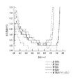
図5に回転角θ2を一定(θ1=+40°)として、あおり角θ1を変化させて欠陥部分を検出させた際の検出信号のS/N比の変化を示す。また、図6に、あおり角θ1を「20°」として、回転角θ2を変化させて欠陥部分を検出させた際の検出信号のS/N比の変化を示す。 FIG. 5 shows a change in the S / N ratio of the detection signal when the rotation angle θ2 is constant (θ1 = + 40 °) and the defect angle is detected by changing the tilt angle θ1. FIG. 6 shows a change in the S / N ratio of the detection signal when the tilt angle θ1 is “20 °” and the rotation angle θ2 is changed to detect a defective portion.
図5に示されるように、回転角θ2を一定としてあおり角θ1を変化させて欠陥を検出させた際には、あおり角θ1の増減に応じて検出信号のS/N比が変化する。そして、あおり角θ1が15°〜35°の範囲内で、検出信号のS/N比を実用レベル(S/N比=2.0)以上とすることができ、あおり角θ1が20°〜25°の範囲内では、検出信号のS/N比を十分に大きくして輝度が極めて小さい欠陥(後述の故障ランク4)までを検出することが可能である。 As shown in FIG. 5, when a defect is detected by changing the tilt angle θ1 while keeping the rotation angle θ2 constant, the S / N ratio of the detection signal changes according to the increase / decrease of the tilt angle θ1. The S / N ratio of the detection signal can be set to a practical level (S / N ratio = 2.0) or more within the range of the tilt angle θ1 of 15 ° to 35 °, and the tilt angle θ1 is set to 20 ° to 20 °. Within a range of 25 °, it is possible to detect even a defect (failure rank 4 to be described later) having a very low luminance by sufficiently increasing the S / N ratio of the detection signal.
すなわち、あおり角θ1が15°〜35°の範囲では、地合検出光に対して欠陥検出光を大きくし、欠陥検出光であるか否かを十分に弁別することができ、20°〜25°の範囲内では極めて微弱な欠陥検出光までを弁別することができる。しかし、あおり角θ1が15°よりも小さい場合には、地合検出光が小さくなるがそれと同時に欠陥部分検出光がより小さくなってしまい、またあおり角θ1が35°よりも大きい場合には、欠陥検出光が大きくなるが地合検出光がより大きくなってしまい、いずれの場合にも欠陥検出光であるか否かを弁別することが困難になってしまう。 That is, when the tilt angle θ1 is in the range of 15 ° to 35 °, the defect detection light can be increased with respect to the formation detection light, and whether or not it is the defect detection light can be sufficiently distinguished. Within the range of °, even very weak defect detection light can be discriminated. However, when the tilt angle θ1 is smaller than 15 °, the ground detection light becomes small, but at the same time, the defect portion detection light becomes smaller, and when the tilt angle θ1 is larger than 35 °, Although the defect detection light becomes large, the ground detection light becomes larger, and in any case, it becomes difficult to discriminate whether or not the defect detection light is.
また、図6に示されるように、回転角θ2に応じて検出信号のS/比が変化し、−60°〜−20°、+20°〜+60°の範囲のときに、欠陥を確実に検出できる実用レベル(S/N比=2.0)以上の検出信号が得られ、−60°〜−30°、+30°〜+60°の範囲内では、検出信号のS/N比を十分に大きく輝度が極めて小さい欠陥(故障ランク4)までを検出することが可能である。なお、回転角θ2の正負は、図4において基準線Lmから反時計方向に回転させた方向を「正」、時計方向に回転させた方向を「負」としてある。 Further, as shown in FIG. 6, the S / ratio of the detection signal changes according to the rotation angle θ2, and the defect is reliably detected when the range is from −60 ° to −20 °, + 20 ° to + 60 °. A detection signal with a practical level (S / N ratio = 2.0) or higher that can be obtained is obtained, and within a range of −60 ° to −30 ° and + 30 ° to + 60 °, the S / N ratio of the detection signal is sufficiently large. It is possible to detect even defects with a very low luminance (failure rank 4). The positive / negative sign of the rotation angle θ2 is defined as “positive” when rotated counterclockwise from the reference line Lm in FIG. 4 and “negative” when rotated clockwise.
そこで、欠陥を精度良く検出するために、上記のようにあおり角θ1を15°〜35°の範囲内の角度に、回転角θ2を20°〜60°の範囲内の角度に設定するようにしており、より好ましくは、あおり角θ1を20°〜25°の範囲内の角度とし、回転角θ2を30°〜60°としている。なお、あおり角θ1を大きくした場合には、視角依存性による1ライン分の検出信号の傾きが大きくなって検出エリア17内での欠陥の検出に影響を与える。この点からもあおり角θ1を20°とするのは特に好ましい。
Therefore, in order to detect defects with high accuracy, the tilt angle θ1 is set to an angle in the range of 15 ° to 35 ° and the rotation angle θ2 is set to an angle in the range of 20 ° to 60 ° as described above. More preferably, the tilt angle θ1 is set to an angle in the range of 20 ° to 25 °, and the rotation angle θ2 is set to 30 ° to 60 °. When the tilt angle θ1 is increased, the inclination of the detection signal for one line due to the viewing angle dependency is increased, which affects the detection of defects in the
回転角θ2の基準となる基準線Lmは、遅相軸xに対して、時計方向、反時計方向のいずれの方向にも90°をなすように設定することができるので、上記角度範囲を満たす位置は回転対称に4カ所(範囲)あり、いずれの位置に受光器16をおいても検査を行うことができるが、より確実に欠陥を検出するためには、検査対象フイルム7の透過光量が多くなる側に受光器16を配置するのがよい。
Since the reference line Lm serving as a reference for the rotation angle θ2 can be set to be 90 ° in either the clockwise direction or the counterclockwise direction with respect to the slow axis x, the above angle range is satisfied. There are four positions (ranges) in rotational symmetry, and inspection can be performed with the
すなわち、検査対象フイルム7が負の一軸性複屈折を示す場合には、図7(a)に示すように、受光器16の光軸Pと交差する遅相軸xを境界にして、受光器16が配されたフイルム面から外に向かって伸びる検査対象フイルム7の光学軸Nが正射影される側の範囲θaで回転角θ2を与えるように、受光器16を配置するのがよい。一方、検査対象フイルム7が正の一軸性複屈折を示す場合には、図7(b)に示すように、受光器16の光軸Pと交差する遅相軸xを境界にして、受光器16が配されたフイルム面から外に向かって伸びる検査対象フイルム7の光学軸Nが正射影される側と反対側の範囲θbで回転角θ2を与えるようにするのがよい。
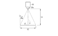
That is, when the
図8に模式的に示すように、受光器16は、その撮影レンズ16aの焦点距離に応じて検査対象フイルム7との受光距離L1を調整することにより、検査エリア17が所定の検査幅L2(この例では250mm)となるように調整されるが、撮影レンズ16aの焦点距離を長くして検査対象フイルム7との受光距離L1を大きくとり、検査エリア17から受光器16を望む方向と光軸Pとのなす最大角φができるだけ小さくするのがよく、3°〜10°の範囲内、より好ましくは3°〜5°の範囲内となるように設定するのが好ましい。なお、図8では、説明のために、受光器16を望む方向と光軸Pに平行な直線Lpとのなす最大角φを示してある。
As schematically shown in FIG. 8, the
このように最大角φを設定するのは、検査対象フイルム7のように複屈折特性を有するフイルムからの光を受光器16で受光する場合の視角依存性の影響を少なくして精度良く欠陥を検出するためである。
The maximum angle φ is set in this way by reducing the influence of viewing angle dependency when receiving light from a film having birefringence characteristics, such as the
図9に検査エリア17に対応する1ライン分の検出信号の例を示す。図9(a)は最大角φが3.2°の場合の、図9(b)は最大角φが4.8°の場合の、図9(c)は最大角φが11.8°の場合の1ライン分の検出信号を示している。各最大角φにおける撮影レンズ16aの焦点距離と、受光器16と検査対象フイルム7との受光距離L1との関係は、表1に示す通りである。なお、いずれの場合も検査エリア17の検査幅L2は250mmである。
FIG. 9 shows an example of detection signals for one line corresponding to the

受光器16が出力する1ライン分の検出信号は、一定なレベルとなるのではなく、検出エリア17の一端側に対応する信号レベルが低く、他端側の信号レベルが高くなるように傾きを持っている。このように検出信号が傾くのは、受光器16にあおり角θ1、回転角θ2が与えられている状態で、視角依存性の影響を受けるためであり、検査エリア17が受光器16によって一端側が暗部として、他端側が明部として観察され、傾きが大きくなるとその暗部と明部との差が大きくなることを意味する。
The detection signal for one line output from the
上記のようにして検出信号の傾きは最大角φに応じて変化し、最大角φが大きくなるほどその傾きが大きくなるが、最大角φを一定値よりも大きくすると、受光器16によって観察される暗部と明部との差がその受光器16のラチチユードを超えて端部を信号変化として検出することができなくなってしまい、あるいはラチチユードに制限されて欠陥の信号レベルの変化を検出できなくなってしまう。このため上記のように最大角φを設定している。
As described above, the inclination of the detection signal changes in accordance with the maximum angle φ, and the inclination increases as the maximum angle φ increases. However, when the maximum angle φ is larger than a certain value, it is observed by the
上記欠陥検査装置10の作用について説明する。装置4,5によって製造された位相差フイルムが検査対象フイルム7として検査装置10に送り込まれ、検査ステージを通って、さらに下流へと搬送される。この搬送中には、光源部15からの光が第1偏光板18を介してフイルム7に照射され、検査対象フイルム7が一定長送られるごとに受光器16で1ライン分の撮影が行われる。
The operation of the
1ライン分の撮影を行うごとに受光器16からは1ライン分の検出信号が出力され、その検出信号が判定装置21に順次に送られる。そして、この判定装置21により、欠陥の有無が判定されるとともに、その欠陥の箇所が特定される。例えばフイルム7の欠陥がある部分では、正常な部分よりも検出信号が高くなり、それが欠陥として判定され、その欠陥の検査対象フイルム7の長手方向と幅方向の各位置情報が出力装置23によって出力されるとともに、後工程に送られる。
Each time one line is photographed, a detection signal for one line is output from the
上記のように、第1偏光板18を介して照明された検査対象フイルム7から射出された光のうち第2偏光板19を透過した光成分をあおり角θ1、回転角θ2を持たせて配置した受光器16によって受光して得られる検出信号に基づいて欠陥の判定を行っているので、微細な欠陥を精度良く検出することができる。
As described above, the light component transmitted through the second
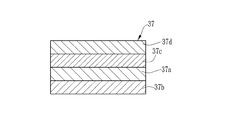
次に第2実施形態について説明する。なお、以下に説明する他は、第1実施形態と同じであり、同じ構成部材には同一の符号を付してその説明を省略する。図10に一例を示すように、検査対象フイルム37は、透明なベースフイルム37aの一方の面に、液晶化合物層37bを、他方の面に偏光子層37cを形成してあり、偏光子層37cの表面に透明な保護フイルム37dを形成してある。ベースフイルム37aと液晶化合物層37bとは、第1実施形態の検査対象フイルム7と同等なものとなっており、光学軸がフイルム面の法線に対して傾斜した正または負の一軸性複屈折を示すフイルムとなっている。
Next, a second embodiment will be described. In addition, except being demonstrated below, it is the same as 1st Embodiment, The same code | symbol is attached | subjected to the same structural member, and the description is abbreviate | omitted. As shown in FIG. 10, the
このような検査対象フイルム37は、例えば例えばヨウ素でPVA(ポリビニールアルコール)フイルムを染色した後にそのPVAフイルムを延伸することにより製造される偏光子層37cとなる偏光フイルムの表面に保護フイルム37dが貼り合わせられたフイルムを作成し、そのフイルムに液晶化合物層37bを形成したベースフイルム37aを貼り合わせることによって製造されている。なお、検査対象フイルム37の製造方法は限られるものではない。
Such a
図11に上記検査対象フイルム37の欠陥を検査する欠陥検査装置38を示す。欠陥検査装置38は、検査対象フイルム37の偏光子層37cを一方の偏光板として用いるため、検査ステージには第1偏光板18を配してあるが、第2偏光板19を設けていない。また、検査対象フイルム37が偏光子層37cを上に向けた姿勢で検査ステージを搬送されるようにしてあり、このときの偏光子層37cと第1偏光板18とがクロスニコル配置となるように第1偏光板18の偏光透過軸の向きを決めてある。
FIG. 11 shows a
偏光子層37cまたは第1偏光板18のいずれか一方が検査対象フイルム37の遅相軸に対して略平行としてある。上記のように検査対象フイルム37を製造する場合には、一般的には、偏光子層37cの偏光透過軸と、検査対象フイルム37の遅相軸とが実質的に平行となるように製造されるので、それに合わせて第1偏光板18の透過軸方向を決定すればよい。もちろん、偏光子層37cの偏光透過軸が検査対象フイルム37の遅相軸と直交する方向とされている場合では、第1偏光板18の透過軸方向が検査対象フイルム37の遅相軸と平行となるように配置すればよい。
Either the
受光器16に関するあおり角θ1,回転角θ2,検査エリア17から受光器16を望む方向と光軸Pとのなす最大角φ等の条件は、第1実施形態と同様である。また、第1偏光板18と偏光子層37cは、第1実施形態における第1,第2偏光板と同様に、第1偏光板18と偏光子層37cは、偏光子層37cとクロスニコル配置となるように検査対象フイルムの液晶化合物層側に第1偏光板18を配した状態で測定される波長500nm〜750nmにおける平均直交透過率が0.027%以下、波長750nmにおける直交透過率が0.030%以下を満たすものを用いることが好ましい。
The conditions such as the tilt angle θ1, the rotation angle θ2, the direction in which the
以上のように構成することにより、第1実施形態と同様に検査対象フイルム37の欠陥を検出することが可能である。なお、検査対象フイルム37としては、正または負の一軸性複屈折を示すものであれば、液晶化合物層を形成したものに限られるものではない。
By configuring as described above, it is possible to detect a defect in the
実施例1〜4として、第1実施形態のように欠陥検査装置10を構成し、前述のような装置4,5で作成され、透過型の光学補償フイルムとして利用される位相差フイルムを検査対象フイルム7として、第1,第2偏光板18,19としての直交透過率の異なる偏光板A〜Dを用いて欠陥、すなわち液晶化合物層の局所的な光学軸のズレに起因して発生する欠陥の検出を行った。各実施例では、第1,第2偏光板18,19には同じ種類の偏光板を使用した。
As Examples 1 to 4, the
実施例1〜4では、あおり角θ1を20°、回転角θ2を40°とし、光源部15として、ハロゲンランプからの光をライトガイドを通して照射するものを用いた。この光源部15の分光分布は図12に示すようなものであった。
In Examples 1 to 4, the tilt angle θ1 is set to 20 °, the rotation angle θ2 is set to 40 °, and the
各偏光板A〜Dの直交透過率の波長分布特性を測定したグラフを図13に示し、透過率のスケールを変更して750nm付近の透過率の違いを明確化したグラフを図14に示す。また、各偏光板A〜Dの570nm〜750nmの波長域の光に対する平均直交透過率、及び波長750nmの光に対する直交透過率を表2に示す。図13,図14及び表2に示す各直交透過率は、同じ種類の一対の偏光板をクロスニコル配置し、それらの間に検査対象フイルム37を配した状態で測定したものであり、第1偏光板18と第2偏光板19とをクロスニコル配置し、それらの間に検査対象フイルム37を配した状態で測定した直交透過率になる。また、図13では、各偏光板の間に検査対象フイルム7を配しない状態で測定した結果をあわせて描いてある。
FIG. 13 shows a graph obtained by measuring the wavelength distribution characteristics of the orthogonal transmittances of the respective polarizing plates A to D, and FIG. 14 shows a graph in which the difference in transmittance around 750 nm is clarified by changing the transmittance scale. Table 2 shows the average orthogonal transmittance for light in the wavelength region of 570 nm to 750 nm and the orthogonal transmittance for light at a wavelength of 750 nm. Each of the orthogonal transmittances shown in FIGS. 13, 14 and Table 2 is measured in a state where a pair of polarizing plates of the same type are arranged in a crossed Nicol state and an
また、比較例5,6として、実施例1,4とに用いた各偏光板A,Dを用い、特許文献5に記載された構成で欠陥の検出を実施した。すなわち、一対の偏光板Aまたは偏光板Dを検査対象フイルム7を挟んで平行に配置するとともに、検査対象フイルム7の遅相軸に対して一方の偏光板の偏光透過軸を適当な交差角をつけて配置した。また、検査対象フイルム7と実質同等の光学補償フイルムを一方の偏光板とフイルムとの間に配置し、フイルム面の法線方向からCCDカメラによって受光を行う構成としている。なお、検査対象フイルム7の遅相軸に対する一方の偏光板の偏光透過軸とのなす交差角は15°、偏光板とフイルムとの間の光学補償フイルムは、フイルム面内で180°回転させた状態に配した。また、光源は、実施例1〜4と同じものを用いた。
Further, as Comparative Examples 5 and 6, the respective polarizing plates A and D used in Examples 1 and 4 were used, and defects were detected with the configuration described in Patent Document 5. That is, a pair of polarizing plates A or D are arranged in parallel with the
実施例1〜4では、受光器16としては、白黒タイプのCCDラインセンサを用い、比較例5,6では、CCDカメラとして、実施例1〜4の受光器16として用いたものと同じCCDラインセンサを用いた。このCCDラインセンサの分光感度特性を図15に示す。
In Examples 1 to 4, a black-and-white type CCD line sensor is used as the
実施例と比較例1〜6の検出結果を表3に示す。表3の故障ランク1〜4は、欠陥箇所とその周囲の濃淡(輝度)の差によって欠陥の程度を示したものであり、故障ランク1が最も濃淡差が大きく、故障ランク2,故障ランク3,故障ランク4の順に濃淡差が小さくなる。 Table 3 shows the detection results of Examples and Comparative Examples 1 to 6. The failure ranks 1 to 4 in Table 3 indicate the degree of the defect by the difference in density (brightness) between the defect location and the surrounding area. The failure rank 1 has the largest difference in shade, and the failure rank 2 and the failure rank 3 , The difference in shade becomes smaller in order of failure rank 4.
上記表3からわかるように、本発明の構成の実施例1〜4は、いずれも故障ランク1,2の欠陥を検出することができ、波長500nm〜750nmにおける平均直交透過率が0.027%であり、波長750nmにおける直交透過率が0.030%である偏光板Dを第1,第2偏光板18,19として用いた実施例4では、極めて欠陥の程度が低い故障ランク4までを良好に検出することができた。これに対して、実施例1と同じ偏光板Aを用いた比較例5、実施例4と同じ偏光板Dを用いた比較例6では、故障ランク1〜4のいずれの欠陥をも検出することができなかった。
As can be seen from Table 3 above, each of Examples 1 to 4 of the configuration of the present invention can detect defects of failure ranks 1 and 2, and the average orthogonal transmittance at wavelengths of 500 nm to 750 nm is 0.027%. In Example 4 in which the polarizing plate D having an orthogonal transmittance of 0.030% at a wavelength of 750 nm was used as the first and second
以上のことから、本発明の構成が光学軸のズレに起因して発生する欠陥に対して有効であることが確認でき、また波長500nm〜750nmにおける平均直交透過率、および特定波長(750nm)における直交透過率が低いほど輝度が低い欠陥をより良好に検出できることが推定されることから、波長500nm〜750nmにおける平均直交透過率が0.027%以下、また波長750nmにおける直交透過率が0.030%以下であることが微細な光漏れ欠陥の検出に有用であることも確認できる。光源をハロゲン光源とした場合には、図12に示す通り、ハロゲン光源の相対強度が波長550〜630nmに極大値を持ち、かつ、波長700〜800nmでも相対強度を有することから、微細な光漏れ欠陥の検出により有用である。 From the above, it can be confirmed that the configuration of the present invention is effective against defects generated due to the deviation of the optical axis, and the average orthogonal transmittance at a wavelength of 500 nm to 750 nm and at a specific wavelength (750 nm). Since it is presumed that defects with lower luminance can be detected better as the orthogonal transmittance is lower, the average orthogonal transmittance at a wavelength of 500 nm to 750 nm is 0.027% or less, and the orthogonal transmittance at a wavelength of 750 nm is 0.030. % Or less can also be confirmed to be useful for detecting fine light leakage defects. When the light source is a halogen light source, as shown in FIG. 12, the relative intensity of the halogen light source has a maximum value at a wavelength of 550 to 630 nm, and also has a relative intensity at a wavelength of 700 to 800 nm. Useful for detecting defects.
7,37 検査対象フイルム
10,39 欠陥検査装置
15 光源部
16 受光器
18,19 偏光板
7, 37 Film to be inspected 10, 39
Claims (15)
検査対象フイルムの一方の面側に配置された第1の偏光板と検査対象フイルムの他方の面側に配置された第2の偏光板とからなり、各偏光板が前記フイルム面と平行とされるとともに、いずれか一方の偏光板の偏光透過軸が検査対象フイルムの遅相軸に対して略平行であり、各偏光板がクロスニコル配置とされた偏光ユニットと、
検査対象フイルムの一方の面側に配置され、前記第1の偏光板を介して検査対象フイルム上のライン状の検査エリアに光を照射する光源と、
検査対象フイルムの他方の面側に配置され、検査対象フイルムから射出され前記第2の偏光板を透過した前記光源からの光を受光して光電信号を出力する受光手段とを備え、
前記受光手段は、複数の受光素子をライン状に配列したラインセンサを有し、前記ラインセンサに対応した前記検査エリアからの光を受光するとともに、その光軸とフイルム面の法線とのなすあおり角θ1、及び前記光軸とフイルム面上における検査対象フイルムの遅相軸に直交する基準線とのなす回転角θ2が、「15°≦θ1≦35°」、「20°≦θ2≦60°」の条件を満たす位置に配され、前記検査エリアが検査対象フイルムの幅方向に対して傾けられていることを特徴とするフイルムの欠陥検査装置。 In a defect inspection apparatus for a film for inspecting defects caused by a deviation of the optical axis of the film based on a photoelectric signal obtained by optically detecting a film to be inspected,
It consists of a first polarizing plate arranged on one surface side of the inspection object film and a second polarizing plate arranged on the other surface side of the inspection object film, and each polarizing plate is parallel to the film surface. And a polarizing unit in which the polarization transmission axis of one of the polarizing plates is substantially parallel to the slow axis of the film to be inspected, and each polarizing plate has a crossed Nicol arrangement,
A light source that is disposed on one surface side of the inspection target film and that irradiates light onto a line-shaped inspection area on the inspection target film via the first polarizing plate;
A light receiving means disposed on the other surface side of the inspection target film, receiving light from the light source that is emitted from the inspection target film and transmitted through the second polarizing plate, and outputs a photoelectric signal;
The light receiving means has a line sensor in which a plurality of light receiving elements in a line, with receiving light from said inspection area corresponding to the line sensor, formed by the normal line of the optical axis and the film plane The tilt angle θ1 and the rotation angle θ2 between the optical axis and the reference line orthogonal to the slow axis of the film to be inspected on the film surface are “15 ° ≦ θ1 ≦ 35 °”, “20 ° ≦ θ2 ≦ 60”. A defect inspection apparatus for a film, wherein the inspection area is tilted with respect to the width direction of the film to be inspected.
検査対象フイルムの偏光子層と反対の他方の面側に配置され、前記偏光子層とクロスニコル配置となるようにされた偏光板と、
検査対象フイルムの他方の面側に配置されて前記偏光板を介して検査対象フイルム上のライン状の検査エリアに光を照射し、または検査対象フイルムの一方の面側に配置されて検査対象フイルム上のライン状の検査エリアに光を照射する光源と、
検査対象フイルムを挟んで前記光源と反対側に配置され、前記偏光板を介して検査対象フイルムに入射し前記偏光子層側から射出される光を受光し、または前記偏光子層側から検査対象フイルムに入射し他方の面から射出される光を受光して光電信号を出力する受光手段とを備え、
前記受光手段は、複数の受光素子をライン状に配列したラインセンサを有し、前記ラインセンサに対応した前記検査エリアからの光を受光するとともに、その光軸とフイルム面の法線とのなすあおり角θ1、及び前記光軸とフイルム面上における検査対象フイルムの遅相軸に直交する基準線とのなす回転角θ2が、「15°≦θ1≦35°」、「20°≦θ2≦60°」の条件を満たす位置に配され、前記検査エリアが検査対象フイルムの幅方向に対して傾けられていることを特徴とするフイルムの欠陥検査装置。 A polarizer layer is formed on one side, and a film whose polarization transmission axis of the polarizer layer is substantially parallel to the slow axis is used as an inspection target film, and the inspection target film is inspected based on a photoelectric signal optically detected. In a defect inspection apparatus for a film for inspecting a defect caused by a deviation of an optical axis of a target film,
A polarizing plate disposed on the other surface side opposite to the polarizer layer of the film to be inspected, and configured to be in a crossed Nicol arrangement with the polarizer layer;
Light is applied to the line-shaped inspection area on the inspection target film via the polarizing plate and arranged on the other surface side of the inspection target film, or the inspection target film is arranged on one surface side of the inspection target film. A light source for irradiating light on the upper line-shaped inspection area ;
It is arranged on the opposite side of the light source across the inspection target film, receives light that enters the inspection target film through the polarizing plate and exits from the polarizer layer side, or is inspected from the polarizer layer side A light receiving means for receiving light incident on the film and emitted from the other surface and outputting a photoelectric signal;
The light receiving means has a line sensor in which a plurality of light receiving elements in a line, with receiving light from said inspection area corresponding to the line sensor, formed by the normal line of the optical axis and the film plane The tilt angle θ1 and the rotation angle θ2 between the optical axis and the reference line orthogonal to the slow axis of the film to be inspected on the film surface are “15 ° ≦ θ1 ≦ 35 °”, “20 ° ≦ θ2 ≦ 60”. A defect inspection apparatus for a film, wherein the inspection area is tilted with respect to the width direction of the film to be inspected.
検査対象のフイルムを挟んで平行に配置された一対の偏光手段のうちの一方を介してフイルム上のライン状の検査エリアに照明光を照射し、このフイルムから射出される光を他方の偏光手段を介して受光手段が受光することによって得られる光電信号に基づいて、フイルムの光学軸のズレに起因した欠陥を検査する検査工程とを有し、
前記検査工程では、前記一対の偏光手段がクロスニコル配置とされるとともに、いずれか一方の偏光手段の偏光透過軸が検査対象のフイルムの遅相軸に対して略平行とされ、前記受光手段が、その光軸とフイルム面の法線とのなすあおり角θ1、及び前記光軸とフイルム面上における検査対象フイルムの遅相軸に直交する基準線とのなす回転角θ2が、「15°≦θ1≦35°」、「20°≦θ2≦60°」の条件を満たす位置に配されるとともに、複数の受光素子をライン状に配列したラインセンサによって検査対象フイルムの幅方向に対して傾けられた検査対象フイルム上のライン状の前記検査エリアから射出される光を受光することを特徴とするフイルムの製造方法。 A forming process for forming a film to be inspected;
Illumination light is irradiated to the line-shaped inspection area on the film through one of a pair of polarizing means arranged in parallel across the film to be inspected, and the light emitted from this film is used as the other polarizing means. An inspection process for inspecting defects caused by deviation of the optical axis of the film, based on a photoelectric signal obtained by receiving light through the light receiving means,
In the inspection step, the pair of polarizing means are arranged in a crossed Nicols arrangement, the polarization transmission axis of one of the polarizing means is substantially parallel to the slow axis of the film to be inspected, and the light receiving means The tilt angle θ1 formed between the optical axis and the normal of the film surface, and the rotation angle θ2 formed between the optical axis and the reference line perpendicular to the slow axis of the film to be inspected on the film surface are “15 ° ≦ It is arranged at a position satisfying the conditions of “θ1 ≦ 35 °” and “20 ° ≦ θ2 ≦ 60 °”, and is tilted with respect to the width direction of the inspection target film by a line sensor in which a plurality of light receiving elements are arranged in a line. method for producing a film, characterized by receiving the light emitted from the line-like of the inspection area on the inspected film was.
Priority Applications (4)
| Application Number | Priority Date | Filing Date | Title |
|---|---|---|---|
| JP2006161280A JP4960026B2 (en) | 2006-06-09 | 2006-06-09 | Film defect inspection apparatus and film manufacturing method |
| CN2007101388870A CN101086483B (en) | 2006-06-09 | 2007-06-08 | Apparatus and method for inspecting film defect |
| US11/759,976 US7428049B2 (en) | 2006-06-09 | 2007-06-08 | Apparatus and method for inspecting film defect |
| KR1020070056971A KR101376648B1 (en) | 2006-06-09 | 2007-06-11 | Apparatus and method for inspecting film defect |
Applications Claiming Priority (1)
| Application Number | Priority Date | Filing Date | Title |
|---|---|---|---|
| JP2006161280A JP4960026B2 (en) | 2006-06-09 | 2006-06-09 | Film defect inspection apparatus and film manufacturing method |
Publications (3)
| Publication Number | Publication Date |
|---|---|
| JP2007327915A JP2007327915A (en) | 2007-12-20 |
| JP2007327915A5 JP2007327915A5 (en) | 2009-11-26 |
| JP4960026B2 true JP4960026B2 (en) | 2012-06-27 |
Family
ID=38821584
Family Applications (1)
| Application Number | Title | Priority Date | Filing Date |
|---|---|---|---|
| JP2006161280A Active JP4960026B2 (en) | 2006-06-09 | 2006-06-09 | Film defect inspection apparatus and film manufacturing method |
Country Status (4)
| Country | Link |
|---|---|
| US (1) | US7428049B2 (en) |
| JP (1) | JP4960026B2 (en) |
| KR (1) | KR101376648B1 (en) |
| CN (1) | CN101086483B (en) |
Families Citing this family (36)
| Publication number | Priority date | Publication date | Assignee | Title |
|---|---|---|---|---|
| JP4217918B2 (en) * | 2006-11-28 | 2009-02-04 | 村田機械株式会社 | Mobile system |
| JP5024935B2 (en) * | 2007-01-16 | 2012-09-12 | 富士フイルム株式会社 | Device and method for detecting defect of light transmitting member |
| KR101057626B1 (en) * | 2008-01-07 | 2011-08-19 | 주식회사 엘지화학 | Polarizer Stain Inspection Method Using Image Analysis and Polarizer Stain Automatic Inspection System Using The Same |
| JP5258349B2 (en) * | 2008-03-28 | 2013-08-07 | 富士フイルム株式会社 | Defect detection apparatus and method |
| KR101676333B1 (en) * | 2008-03-28 | 2016-11-15 | 후지필름 가부시키가이샤 | Method and device for detecting defect |
| JP5175600B2 (en) * | 2008-04-09 | 2013-04-03 | 株式会社日立ハイテクノロジーズ | Inspection device |
| JP2011033564A (en) * | 2009-08-05 | 2011-02-17 | Sumitomo Chemical Co Ltd | Optical film inspection method |
| TW201107817A (en) * | 2009-08-18 | 2011-03-01 | Hirose Tech Co Ltd | Image inspection apparatus |
| CN101806966B (en) * | 2010-03-31 | 2012-05-23 | 苏州达信科技电子有限公司 | Detection device and detection method |
| JP2012163533A (en) * | 2011-02-09 | 2012-08-30 | Fujifilm Corp | Defect inspection apparatus and method for lenticular sheet |
| TWI536003B (en) * | 2011-08-31 | 2016-06-01 | 富士軟片股份有限公司 | Apparatus and method of detecting defect for patterned retardation film and method of manufacturing patterned retardation film |
| KR101294220B1 (en) * | 2011-11-21 | 2013-08-07 | 동우 화인켐 주식회사 | Apparatus for acquiring image of patterned retarder |
| CN102539482B (en) * | 2012-02-09 | 2013-10-23 | 重庆师范大学 | Micro-current detection system for micropore defect of transparent film |
| JP2013205091A (en) * | 2012-03-27 | 2013-10-07 | Dainippon Printing Co Ltd | Film inspection system, and film inspection method |
| JP2013210245A (en) * | 2012-03-30 | 2013-10-10 | Dainippon Printing Co Ltd | Film inspection system, and film inspection method |
| JP5173047B2 (en) * | 2012-05-15 | 2013-03-27 | 株式会社ナナオ | Screen light calculation device or method thereof |
| EP2703772B1 (en) * | 2012-08-28 | 2015-05-20 | Texmag GmbH Vertriebsgesellschaft | Sensor for detecting a moving strip |
| CN110071427B (en) * | 2012-12-28 | 2020-08-21 | 大金工业株式会社 | Polarized resin film and method for producing same |
| KR20140087715A (en) * | 2012-12-31 | 2014-07-09 | 동우 화인켐 주식회사 | Apparatus for in-line measurement |
| KR101446061B1 (en) * | 2013-10-15 | 2014-10-01 | 기가비스주식회사 | Apparatus for measuring a defect of surface pattern of transparent substrate |
| KR101697071B1 (en) * | 2014-04-18 | 2017-01-17 | 동우 화인켐 주식회사 | Method for discriminating defect of polarizing plate |
| CN104317075B (en) * | 2014-10-14 | 2017-10-24 | 深圳市华星光电技术有限公司 | Lighting-up equipment of liquid crystal cell |
| CN105115429B (en) * | 2015-05-26 | 2016-06-29 | 雷艳梅 | A kind of reflective chemical liquid smears uniformity detecting method and device |
| WO2017171153A1 (en) * | 2016-03-31 | 2017-10-05 | 동우화인켐 주식회사 | Polarizing plate inspection method and polarizing plate inspection device |
| US11391678B2 (en) * | 2017-07-28 | 2022-07-19 | Shanjin Optoelectronics (Suzhou) Co., Ltd. | Device and method for detecting defect of optical film |
| JP6924645B2 (en) * | 2017-07-31 | 2021-08-25 | 日東電工株式会社 | Polarizing film imaging device, inspection device, and inspection method |
| JP7095966B2 (en) * | 2017-09-22 | 2022-07-05 | 株式会社Screenホールディングス | Inspection equipment and inspection method |
| CN107703152A (en) * | 2017-10-27 | 2018-02-16 | 深圳精创视觉科技有限公司 | The automatic indication device of optical film shortcoming |
| CN108273768B (en) * | 2018-02-09 | 2020-04-21 | 明基材料有限公司 | Polaroid screening device and method |
| CN109187577A (en) * | 2018-08-29 | 2019-01-11 | 深圳市盛波光电科技有限公司 | A kind of polaroid recessiveness defect light detection means and method |
| CN109540902A (en) * | 2018-11-14 | 2019-03-29 | 苏州襄行软件有限公司 | A kind of polaroid Defect Detection system and its detection method |
| CN110033433B (en) * | 2019-03-04 | 2021-07-02 | 深圳市智能机器人研究院 | Texture defect detection method, system, device and storage medium |
| JP2020173188A (en) * | 2019-04-11 | 2020-10-22 | 住友化学株式会社 | Inspection device, inspection method, and film manufacturing method |
| JP2022072182A (en) * | 2020-10-29 | 2022-05-17 | 住友化学株式会社 | Inspection method |
| CN114324369B (en) * | 2022-03-11 | 2022-06-07 | 北京新研创能科技有限公司 | System and method for detecting scratches on surface of bipolar plate |
| CN116559199A (en) * | 2023-07-10 | 2023-08-08 | 杭州百子尖科技股份有限公司 | Film defect detection device and detection method based on machine vision |
Family Cites Families (11)
| Publication number | Priority date | Publication date | Assignee | Title |
|---|---|---|---|---|
| JPH06235624A (en) | 1992-12-15 | 1994-08-23 | Hitachi Ltd | Inspecting method and apparatus for transparent sheet |
| JP3368512B2 (en) | 1994-08-12 | 2003-01-20 | 住友化学工業株式会社 | Defect inspection method for transparent sheet-like molded product |
| JP3554619B2 (en) | 1995-09-06 | 2004-08-18 | 富士写真フイルム株式会社 | Manufacturing method of long optical compensation sheet |
| JPH1130591A (en) | 1997-07-11 | 1999-02-02 | Asahi Chem Ind Co Ltd | Method and device for inspecting film sheet defect |
| JP3803999B2 (en) * | 1999-08-25 | 2006-08-02 | 富士写真フイルム株式会社 | Defect inspection equipment |
| US6650410B2 (en) * | 2000-03-08 | 2003-11-18 | Fuji Photo Film Co., Ltd. | Apparatus, system and method for checking film for defects |
| JP4440485B2 (en) * | 2000-03-08 | 2010-03-24 | 富士フイルム株式会社 | Film defect inspection apparatus, defect inspection system, defect inspection method, and method for manufacturing film having birefringence characteristics |
| JP2003344301A (en) * | 2002-05-31 | 2003-12-03 | Sumitomo Chem Co Ltd | Method and equipment for inspecting polarization film |
| JP2004198163A (en) * | 2002-12-17 | 2004-07-15 | Sumitomo Chem Co Ltd | Defect inspection method for protective film adhered polarizing plate |
| JP4411139B2 (en) | 2004-05-25 | 2010-02-10 | 新日本石油株式会社 | Optical film inspection method |
| JP4628824B2 (en) | 2005-03-10 | 2011-02-09 | 富士フイルム株式会社 | Film defect inspection apparatus and film manufacturing method |
-
2006
- 2006-06-09 JP JP2006161280A patent/JP4960026B2/en active Active
-
2007
- 2007-06-08 CN CN2007101388870A patent/CN101086483B/en active Active
- 2007-06-08 US US11/759,976 patent/US7428049B2/en not_active Expired - Fee Related
- 2007-06-11 KR KR1020070056971A patent/KR101376648B1/en active IP Right Grant
Also Published As
| Publication number | Publication date |
|---|---|
| KR20070118053A (en) | 2007-12-13 |
| CN101086483A (en) | 2007-12-12 |
| US20070285665A1 (en) | 2007-12-13 |
| JP2007327915A (en) | 2007-12-20 |
| KR101376648B1 (en) | 2014-03-20 |
| US7428049B2 (en) | 2008-09-23 |
| CN101086483B (en) | 2011-08-31 |
Similar Documents
| Publication | Publication Date | Title |
|---|---|---|
| JP4960026B2 (en) | Film defect inspection apparatus and film manufacturing method | |
| JP4628824B2 (en) | Film defect inspection apparatus and film manufacturing method | |
| KR101249119B1 (en) | Layered film fabrication method, layered film defect detection method, layered film defect detection device, layered film, and image display device | |
| JP2007327915A5 (en) | ||
| JP5024935B2 (en) | Device and method for detecting defect of light transmitting member | |
| KR101744606B1 (en) | Film defect inspection device, defect inspection method, and release film | |
| KR20080086929A (en) | Layered film fabrication method, layered film defect detection method, layered film defect detection device, layered film, and image display device | |
| JP2012137502A (en) | Inspection method and manufacturing method for component having double refraction characteristic | |
| JP2008298566A (en) | Apparatus and method for inspecting defect of film | |
| WO2021176797A1 (en) | Inspection method | |
| TW202129263A (en) | Inspection method, inspection apparatus and inspection system | |
| KR20170002220A (en) | uneveness inspection apparatus for polaroid film | |
| TW202129249A (en) | Inspection method, inspection device and inspection system | |
| JP2008267991A (en) | Phase difference film inspecting device, phase difference film inspecting method, and method of manufacturing phase difference film using same | |
| KR20160005445A (en) | Apparatus of inspecting defect of polarizing plate and method of inspecting the same | |
| WO2021124646A1 (en) | Inspection method, inspection device, and inspection system | |
| JP7105925B2 (en) | Contaminant inspection system for display units | |
| WO2022092006A1 (en) | Inspection method | |
| JP2007212330A (en) | Optical anisotropic parameter measuring method and measuring instrument | |
| JP2009025593A (en) | Inspection method of optical compensation plate | |
| CN116519711A (en) | Inspection method | |
| CN115015280A (en) | Defect inspection method and defect inspection apparatus |
Legal Events
| Date | Code | Title | Description |
|---|---|---|---|
| A621 | Written request for application examination |
Free format text: JAPANESE INTERMEDIATE CODE: A621 Effective date: 20090204 |
|
| A521 | Request for written amendment filed |
Free format text: JAPANESE INTERMEDIATE CODE: A523 Effective date: 20091013 |
|
| A131 | Notification of reasons for refusal |
Free format text: JAPANESE INTERMEDIATE CODE: A131 Effective date: 20110518 |
|
| A521 | Request for written amendment filed |
Free format text: JAPANESE INTERMEDIATE CODE: A523 Effective date: 20110719 |
|
| A02 | Decision of refusal |
Free format text: JAPANESE INTERMEDIATE CODE: A02 Effective date: 20110817 |
|
| A521 | Request for written amendment filed |
Free format text: JAPANESE INTERMEDIATE CODE: A523 Effective date: 20111117 |
|
| A911 | Transfer to examiner for re-examination before appeal (zenchi) |
Free format text: JAPANESE INTERMEDIATE CODE: A911 Effective date: 20111222 |
|
| A131 | Notification of reasons for refusal |
Free format text: JAPANESE INTERMEDIATE CODE: A131 Effective date: 20120125 |
|
| A521 | Request for written amendment filed |
Free format text: JAPANESE INTERMEDIATE CODE: A523 Effective date: 20120208 |
|
| TRDD | Decision of grant or rejection written | ||
| A01 | Written decision to grant a patent or to grant a registration (utility model) |
Free format text: JAPANESE INTERMEDIATE CODE: A01 Effective date: 20120314 |
|
| A01 | Written decision to grant a patent or to grant a registration (utility model) |
Free format text: JAPANESE INTERMEDIATE CODE: A01 |
|
| A61 | First payment of annual fees (during grant procedure) |
Free format text: JAPANESE INTERMEDIATE CODE: A61 Effective date: 20120322 |
|
| FPAY | Renewal fee payment (event date is renewal date of database) |
Free format text: PAYMENT UNTIL: 20150330 Year of fee payment: 3 |
|
| R150 | Certificate of patent or registration of utility model |
Ref document number: 4960026 Country of ref document: JP Free format text: JAPANESE INTERMEDIATE CODE: R150 Free format text: JAPANESE INTERMEDIATE CODE: R150 |
|
| R250 | Receipt of annual fees |
Free format text: JAPANESE INTERMEDIATE CODE: R250 |
|
| R250 | Receipt of annual fees |
Free format text: JAPANESE INTERMEDIATE CODE: R250 |
|
| R250 | Receipt of annual fees |
Free format text: JAPANESE INTERMEDIATE CODE: R250 |
|
| R250 | Receipt of annual fees |
Free format text: JAPANESE INTERMEDIATE CODE: R250 |
|
| R250 | Receipt of annual fees |
Free format text: JAPANESE INTERMEDIATE CODE: R250 |
|
| R250 | Receipt of annual fees |
Free format text: JAPANESE INTERMEDIATE CODE: R250 |
|
| R250 | Receipt of annual fees |
Free format text: JAPANESE INTERMEDIATE CODE: R250 |
|
| R250 | Receipt of annual fees |
Free format text: JAPANESE INTERMEDIATE CODE: R250 |
|
| R250 | Receipt of annual fees |
Free format text: JAPANESE INTERMEDIATE CODE: R250 |
|
| R250 | Receipt of annual fees |
Free format text: JAPANESE INTERMEDIATE CODE: R250 |