JP4896830B2 - 磁気ランダムアクセスメモリ - Google Patents
磁気ランダムアクセスメモリ Download PDFInfo
- Publication number
- JP4896830B2 JP4896830B2 JP2007175564A JP2007175564A JP4896830B2 JP 4896830 B2 JP4896830 B2 JP 4896830B2 JP 2007175564 A JP2007175564 A JP 2007175564A JP 2007175564 A JP2007175564 A JP 2007175564A JP 4896830 B2 JP4896830 B2 JP 4896830B2
- Authority
- JP
- Japan
- Prior art keywords
- mosfet
- gate terminal
- resistance state
- transistor
- circuit
- Prior art date
- Legal status (The legal status is an assumption and is not a legal conclusion. Google has not performed a legal analysis and makes no representation as to the accuracy of the status listed.)
- Expired - Fee Related
Links
Images


Classifications
-
- G—PHYSICS
- G11—INFORMATION STORAGE
- G11C—STATIC STORES
- G11C11/00—Digital stores characterised by the use of particular electric or magnetic storage elements; Storage elements therefor
- G11C11/02—Digital stores characterised by the use of particular electric or magnetic storage elements; Storage elements therefor using magnetic elements
- G11C11/14—Digital stores characterised by the use of particular electric or magnetic storage elements; Storage elements therefor using magnetic elements using thin-film elements
- G11C11/15—Digital stores characterised by the use of particular electric or magnetic storage elements; Storage elements therefor using magnetic elements using thin-film elements using multiple magnetic layers
-
- G—PHYSICS
- G11—INFORMATION STORAGE
- G11C—STATIC STORES
- G11C11/00—Digital stores characterised by the use of particular electric or magnetic storage elements; Storage elements therefor
- G11C11/02—Digital stores characterised by the use of particular electric or magnetic storage elements; Storage elements therefor using magnetic elements
- G11C11/16—Digital stores characterised by the use of particular electric or magnetic storage elements; Storage elements therefor using magnetic elements using elements in which the storage effect is based on magnetic spin effect
- G11C11/165—Auxiliary circuits
- G11C11/1673—Reading or sensing circuits or methods
Landscapes
- Engineering & Computer Science (AREA)
- Computer Hardware Design (AREA)
- Hall/Mr Elements (AREA)
- Mram Or Spin Memory Techniques (AREA)
Description
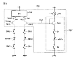
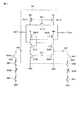
図1乃至図3を参照して、本発明の第1実施形態に係る磁気ランダムアクセスメモリについて説明する。図1は、第1実施形態に係る磁気ランダムアクセスメモリの主要部を概略的に示す回路図である。図1に示すように、メモリセルMCおよび参照セルRCが行列状に配置される。メモリセルMC、直列接続された磁気抵抗効果(MR)素子MRMと選択トランジスタTMとからなる。参照セルRCは、直列接続されたMR素子MRRと選択トランジスタTRとからなる。選択トランジスタTM、TRは、例えば、n型のMOSFET(metal oxide semiconductor field effect transistor)から構成される。
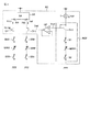
第2実施形態は、トランジスタQn2とトランジスタQn3との接続の仕方に関する。図4は、本発明の第2実施形態に係る磁気ランダムアクセスメモリの主要部を概略的に示す回路図である。図4に示すように、読み出し回路RCにおいて、トランジスタQn3のゲート端子の電位は、ユニティゲインバッファを介して、トランジスタQn2のゲート端子に転送される。
第3実施形態は、第1、第2実施形態の定電流回路Iの具体例に関する。
第4実施形態は、第1、第2実施形態の定電流回路Iの具体例に関する。
第5実施形態は、第1乃至第4実施形態のセンスアンプSAの具体例に関する。
Claims (5)
- 低抵抗状態と前記低抵抗状態よりも高い抵抗値を有する高抵抗状態との2つの定常状態を有する第1磁気抵抗効果素子と、
低抵抗状態と前記低抵抗状態よりも高い抵抗値を有する高抵抗状態との2つの定常状態のいずれか一方に固定された第2磁気抵抗効果素子と、
一端を前記第1磁気抵抗効果素子と接続され、ゲート端子に第1電位を印加された第1MOSFETと、
一端を前記第2磁気抵抗効果素子と接続された第2MOSFETと、
前記第1MOSFETの他端を流れる電流と前記第2MOSFETの他端を流れる電流との差を増幅するセンスアンプと、
低抵抗状態の前記第1磁気抵抗効果素子を流れる電流と、高抵抗状態の前記第1磁気抵抗効果素子を流れる電流と、の間の値を有する参照電流を出力する定電流回路と、
一端において前記参照電流を供給され、前記一端と接続されたゲート端子を有する第3MOSFETと、
前記第3MOSFETの他端と接続され、前記第2磁気抵抗効果素子と実質的に同じ抵抗値を有する第1抵抗素子と、
を具備し、
前記第2MOSFETのゲート端子には、前記第3MOSFETのゲート端子と同じ電位が印加される、
ことを特徴とする磁気ランダムアクセスメモリ。 - 非反転入力端を前記第3MOSFETの前記ゲート端子と接続され、出力端を自身の反転入力端および前記第2MOSFETの前記ゲート端子と接続されたオペアンプをさらに具備することを特徴とする請求項1の磁気ランダムアクセスメモリ。
- 前記定電流回路は、低抵抗状態の前記第1磁気抵抗効果素子と同じ抵抗値を有する第2抵抗素子と、高抵抗状態の前記第1磁気抵抗効果素子と同じ抵抗値を有する第3抵抗素子と、を含む、ことを特徴とする請求項1に記載の磁気ランダムアクセスメモリ。
- 前記定電流回路は、
一端を電源電位端と接続され、他端を自身のゲート端子および前記第3MOSFETの前記一端と接続された第4MOSFETと、
一端を前記電源電位端と接続され、他端を自身のゲート端子および前記第4MOSFETの前記ゲート端子と接続された第5MOSFETと、
一端を前記電源電位端と接続され、他端を自身のゲート端子および前記第4MOSFETの前記ゲート端子と接続された第6MOSFETと、
一端を前記第5MOSFETの前記他端と接続され、他端を前記第2抵抗素子と接続され、ゲート端子に前記第1電位を印加される第7MOSFETと、
一端を前記第6MOSFETの前記他端と接続され、他端を前記第3抵抗素子と接続され、ゲート端子に前記第1電位を印加される第8MOSFETと、
をさらに含むことを特徴とする請求項3に記載の磁気ランダムアクセスメモリ。 - 前記第1磁気抵抗効果素子は、第1強磁性膜と、第2強磁性膜と、前記第1、第2強磁性膜間に設けられた第1非磁性膜と、を含み、
前記第2磁気抵抗効果素子および前記第1乃至第3抵抗素子は、前記第1磁性膜と同じ特性を有する第3強磁性膜と、前記第2強磁性膜と同じ特性を有する第4協磁性膜と、前記第1非磁性膜と同じ特性を有し且つ前記第3、第4強磁性膜間に設けられた第2非磁性膜と、を含み、且つ抵抗状態を固定されている、
ことを特徴とする請求項3に記載の磁気ランダムアクセスメモリ。
Priority Applications (2)
| Application Number | Priority Date | Filing Date | Title |
|---|---|---|---|
| JP2007175564A JP4896830B2 (ja) | 2007-07-03 | 2007-07-03 | 磁気ランダムアクセスメモリ |
| US12/164,410 US7791930B2 (en) | 2007-07-03 | 2008-06-30 | Magnetoresistive random access memory |
Applications Claiming Priority (1)
| Application Number | Priority Date | Filing Date | Title |
|---|---|---|---|
| JP2007175564A JP4896830B2 (ja) | 2007-07-03 | 2007-07-03 | 磁気ランダムアクセスメモリ |
Publications (2)
| Publication Number | Publication Date |
|---|---|
| JP2009015949A JP2009015949A (ja) | 2009-01-22 |
| JP4896830B2 true JP4896830B2 (ja) | 2012-03-14 |
Family
ID=40221289
Family Applications (1)
| Application Number | Title | Priority Date | Filing Date |
|---|---|---|---|
| JP2007175564A Expired - Fee Related JP4896830B2 (ja) | 2007-07-03 | 2007-07-03 | 磁気ランダムアクセスメモリ |
Country Status (2)
| Country | Link |
|---|---|
| US (1) | US7791930B2 (ja) |
| JP (1) | JP4896830B2 (ja) |
Families Citing this family (22)
| Publication number | Priority date | Publication date | Assignee | Title |
|---|---|---|---|---|
| JP5002401B2 (ja) * | 2007-10-03 | 2012-08-15 | 株式会社東芝 | 抵抗変化メモリ |
| JP2010079974A (ja) * | 2008-09-25 | 2010-04-08 | Toshiba Corp | 半導体記憶装置 |
| JP2011003241A (ja) * | 2009-06-18 | 2011-01-06 | Toshiba Corp | 半導体記憶装置 |
| US8213213B2 (en) * | 2009-11-09 | 2012-07-03 | National Tsing Hua University | Reference current generator for resistance type memory and method thereof |
| US8254195B2 (en) * | 2010-06-01 | 2012-08-28 | Qualcomm Incorporated | High-speed sensing for resistive memories |
| US8693273B2 (en) * | 2012-01-06 | 2014-04-08 | Headway Technologies, Inc. | Reference averaging for MRAM sense amplifiers |
| US9111622B2 (en) * | 2012-05-09 | 2015-08-18 | Everspin Technologies, Inc. | Self referencing sense amplifier for spin torque MRAM |
| US9183912B2 (en) | 2012-05-17 | 2015-11-10 | Everspin Technologies, Inc. | Circuit and method for controlling MRAM cell bias voltages |
| WO2014129172A1 (ja) * | 2013-02-19 | 2014-08-28 | パナソニック株式会社 | 不揮発性半導体記憶装置 |
| US8947920B2 (en) | 2013-03-22 | 2015-02-03 | Masahiro Takahashi | Memory device |
| US9177641B2 (en) | 2013-03-22 | 2015-11-03 | Masahiro Takahashi | Memory device |
| US9070440B2 (en) | 2013-08-26 | 2015-06-30 | Masahiro Takahashi | Resistance change memory |
| WO2015132980A1 (en) * | 2014-03-07 | 2015-09-11 | Akira Katayama | Memory device |
| US10043564B2 (en) | 2014-12-10 | 2018-08-07 | Toshiba Memory Corporation | Semiconductor memory device and method of controlling semiconductor memory device |
| US9502106B2 (en) | 2014-12-10 | 2016-11-22 | Kabushiki Kaisha Toshiba | Semiconductor memory device and method of controlling semiconductor memory device |
| US9747966B2 (en) * | 2015-08-25 | 2017-08-29 | Toshiba Memory Corporation | Semiconductor memory device for sensing memory cell with variable resistance |
| US9679643B1 (en) * | 2016-03-09 | 2017-06-13 | Taiwan Semiconductor Manufacturing Co., Ltd. | Resistive memory device having a trimmable resistance of at least on of a driver and a sinker is trimmed based on a row location |
| JP6574862B1 (ja) * | 2018-03-15 | 2019-09-11 | 株式会社東芝 | メモリ装置 |
| US10839879B2 (en) * | 2018-09-27 | 2020-11-17 | Taiwan Semiconductor Manufacturing Co., Ltd. | Read techniques for a magnetic tunnel junction (MTJ) memory device with a current mirror |
| US10803913B1 (en) * | 2019-06-11 | 2020-10-13 | Applied Materials, Inc. | Narrow range sense amplifier with immunity to noise and variation |
| US10796741B1 (en) * | 2019-10-30 | 2020-10-06 | Nxp Usa, Inc. | Non-volatile memory with a select gate regulator circuit |
| DE102020109378A1 (de) | 2020-04-03 | 2021-10-07 | Infineon Technologies Ag | Leseschaltung für Resistive-Change-Speicher |
Family Cites Families (9)
| Publication number | Priority date | Publication date | Assignee | Title |
|---|---|---|---|---|
| US5608676A (en) * | 1993-08-31 | 1997-03-04 | Crystal Semiconductor Corporation | Current limited current reference for non-volatile memory sensing |
| US6385109B1 (en) * | 2001-01-30 | 2002-05-07 | Motorola, Inc. | Reference voltage generator for MRAM and method |
| US6944048B2 (en) * | 2001-11-29 | 2005-09-13 | Kabushiki Kaisha Toshiba | Magnetic random access memory |
| JP2003173700A (ja) * | 2001-12-03 | 2003-06-20 | Mitsubishi Electric Corp | 半導体記憶装置 |
| US6600690B1 (en) * | 2002-06-28 | 2003-07-29 | Motorola, Inc. | Sense amplifier for a memory having at least two distinct resistance states |
| US6700814B1 (en) * | 2002-10-30 | 2004-03-02 | Motorola, Inc. | Sense amplifier bias circuit for a memory having at least two distinct resistance states |
| JP2006210396A (ja) * | 2005-01-25 | 2006-08-10 | Fujitsu Ltd | 磁気メモリ装置及びその読み出し方法 |
| US7313043B2 (en) * | 2005-11-29 | 2007-12-25 | Altis Semiconductor Snc | Magnetic Memory Array |
| US7495971B2 (en) * | 2006-04-19 | 2009-02-24 | Infineon Technologies Ag | Circuit and a method of determining the resistive state of a resistive memory cell |
-
2007
- 2007-07-03 JP JP2007175564A patent/JP4896830B2/ja not_active Expired - Fee Related
-
2008
- 2008-06-30 US US12/164,410 patent/US7791930B2/en active Active
Also Published As
| Publication number | Publication date |
|---|---|
| US7791930B2 (en) | 2010-09-07 |
| US20090010045A1 (en) | 2009-01-08 |
| JP2009015949A (ja) | 2009-01-22 |
Similar Documents
| Publication | Publication Date | Title |
|---|---|---|
| JP4896830B2 (ja) | 磁気ランダムアクセスメモリ | |
| JP4768770B2 (ja) | 半導体記憶装置 | |
| Chen et al. | A 130 nm 1.2 V/3.3 V 16 Kb spin-transfer torque random access memory with nondestructive self-reference sensing scheme | |
| JP5422665B2 (ja) | 固定されていない基準層および一方向書込電流を有するスピントルクビットセル | |
| US7760543B2 (en) | Resistance change memory | |
| US6930911B2 (en) | Magnetic memory device, method for writing on the same and method for reading from the same | |
| CN111755050A (zh) | 非易失性存储器件 | |
| US7688623B2 (en) | Magnetic memory cell and magnetic memory device | |
| US7511992B2 (en) | Magnetic memory device | |
| US20070291531A1 (en) | Mram with a write driver and a method therefor | |
| JP4283011B2 (ja) | 磁気メモリデバイスおよびその読出方法 | |
| CN108630262A (zh) | 半导体存储装置 | |
| EP3945521A1 (en) | Magnetic random access memory cell and method for reading said cell | |
| JP4361067B2 (ja) | Mramメモリセル | |
| US8514614B2 (en) | Magnetic memory | |
| CN111128265B (zh) | 磁性隧道结读取电路、装置以及读取磁性隧道结的方法 | |
| CN106796815B (zh) | 非易失性半导体存储器 | |
| TWI537947B (zh) | 磁阻記憶體裝置 | |
| CN109935273B (zh) | 一种对mtj电阻进行筛选的电路 | |
| JP3808835B2 (ja) | 半導体装置間信号伝送システム | |
| JP2011198416A (ja) | 磁気メモリ | |
| JP2003085968A (ja) | 磁気メモリ装置の読み出し回路 | |
| JP4741758B2 (ja) | 磁気メモリ装置の読み出し回路 | |
| JP2012256388A (ja) | 半導体装置 | |
| JP2012069694A (ja) | 磁気メモリ |
Legal Events
| Date | Code | Title | Description |
|---|---|---|---|
| A621 | Written request for application examination |
Free format text: JAPANESE INTERMEDIATE CODE: A621 Effective date: 20090806 |
|
| A977 | Report on retrieval |
Free format text: JAPANESE INTERMEDIATE CODE: A971007 Effective date: 20111109 |
|
| TRDD | Decision of grant or rejection written | ||
| A01 | Written decision to grant a patent or to grant a registration (utility model) |
Free format text: JAPANESE INTERMEDIATE CODE: A01 Effective date: 20111129 |
|
| A01 | Written decision to grant a patent or to grant a registration (utility model) |
Free format text: JAPANESE INTERMEDIATE CODE: A01 |
|
| A61 | First payment of annual fees (during grant procedure) |
Free format text: JAPANESE INTERMEDIATE CODE: A61 Effective date: 20111221 |
|
| FPAY | Renewal fee payment (event date is renewal date of database) |
Free format text: PAYMENT UNTIL: 20150106 Year of fee payment: 3 |
|
| LAPS | Cancellation because of no payment of annual fees |