JP4896830B2 - Magnetic random access memory - Google Patents
Magnetic random access memory Download PDFInfo
- Publication number
- JP4896830B2 JP4896830B2 JP2007175564A JP2007175564A JP4896830B2 JP 4896830 B2 JP4896830 B2 JP 4896830B2 JP 2007175564 A JP2007175564 A JP 2007175564A JP 2007175564 A JP2007175564 A JP 2007175564A JP 4896830 B2 JP4896830 B2 JP 4896830B2
- Authority
- JP
- Japan
- Prior art keywords
- mosfet
- gate terminal
- resistance state
- transistor
- circuit
- Prior art date
- Legal status (The legal status is an assumption and is not a legal conclusion. Google has not performed a legal analysis and makes no representation as to the accuracy of the status listed.)
- Expired - Fee Related
Links
Images


Classifications
-
- G—PHYSICS
- G11—INFORMATION STORAGE
- G11C—STATIC STORES
- G11C11/00—Digital stores characterised by the use of particular electric or magnetic storage elements; Storage elements therefor
- G11C11/02—Digital stores characterised by the use of particular electric or magnetic storage elements; Storage elements therefor using magnetic elements
- G11C11/14—Digital stores characterised by the use of particular electric or magnetic storage elements; Storage elements therefor using magnetic elements using thin-film elements
- G11C11/15—Digital stores characterised by the use of particular electric or magnetic storage elements; Storage elements therefor using magnetic elements using thin-film elements using multiple magnetic layers
-
- G—PHYSICS
- G11—INFORMATION STORAGE
- G11C—STATIC STORES
- G11C11/00—Digital stores characterised by the use of particular electric or magnetic storage elements; Storage elements therefor
- G11C11/02—Digital stores characterised by the use of particular electric or magnetic storage elements; Storage elements therefor using magnetic elements
- G11C11/16—Digital stores characterised by the use of particular electric or magnetic storage elements; Storage elements therefor using magnetic elements using elements in which the storage effect is based on magnetic spin effect
- G11C11/165—Auxiliary circuits
- G11C11/1673—Reading or sensing circuits or methods
Landscapes
- Engineering & Computer Science (AREA)
- Computer Hardware Design (AREA)
- Mram Or Spin Memory Techniques (AREA)
- Hall/Mr Elements (AREA)
Description
本発明は、磁気ランダムアクセスメモリに関し、例えば磁気ランダムアクセスメモリの読み出し回路構成に関する。 The present invention relates to a magnetic random access memory, for example, a read circuit configuration of a magnetic random access memory.
磁気ランダムアクセスメモリ(MRAM)は、高速アクセスが可能な不揮発性メモリである。MRAMは、磁気抵抗効果(MR)素子を利用して情報を記憶する。MR素子は、磁化の状態に応じて、例えば2つの異なる抵抗値を取る。読み出しは、MR素子の抵抗値を判別することによって行われる。よって、MR素子の抵抗値を精度良く検出する読出し方法が必要とされる。 Magnetic random access memory (MRAM) is a non-volatile memory that can be accessed at high speed. The MRAM stores information using a magnetoresistive effect (MR) element. The MR element takes, for example, two different resistance values depending on the state of magnetization. Reading is performed by determining the resistance value of the MR element. Therefore, a reading method for accurately detecting the resistance value of the MR element is required.
読み出し方法の1つとして差動増幅方式がある。差動増幅方式では、情報記憶用のメモリセル内のMR素子の抵抗状態に応じた値の読み出し信号電流が、参照電流と比較され、2つの電流値の差を増幅する。参照信号は、相互に抵抗値の異なる複数の参照セル用MR素子を組み合わせることで、メモリセル用のMR素子の2つの抵抗値の中間の抵抗値を用いて、得る方法が知られている。しかし、この方法では1つの参照信号を生成するのに複数の参照セルを必要とする。このため、メモリセルアレイ内に配置される参照セルの数が多くなり、メモリセルのメモリセルアレイにおける占有率が低下する。 There is a differential amplification method as one of the reading methods. In the differential amplification method, the read signal current having a value corresponding to the resistance state of the MR element in the memory cell for information storage is compared with the reference current, and the difference between the two current values is amplified. A method is known in which a reference signal is obtained by combining a plurality of MR elements for reference cells having different resistance values and using a resistance value intermediate between two resistance values of the MR elements for memory cells. However, this method requires a plurality of reference cells to generate one reference signal. For this reason, the number of reference cells arranged in the memory cell array increases, and the occupation ratio of the memory cells in the memory cell array decreases.
この問題を回避する技術として、1つの参照セルで参照信号を生成する方法が特許文献1に公開されている。この方法では、メモリセルに印加される読み出しバイアス電圧と、参照セルに印加される読み出しバイアス電圧と、を異ならせる。そして、参照セルを流れる参照電流の値が、セル用の磁気抵抗素子の2つの抵抗値のそれぞれにおける計2つの読み出し信号電流の中間になるように設定される。具体的には、メモリセルに印加されるバイアス電圧をVbias1、メモリセルの低い方の抵抗値をRmin、高い方の抵抗値Rmaxとして、参照セルに印加されるバイアス電圧を(Vbias1/2)(1+Rmin/Rmax)とする。そして、参照セルの抵抗値がRmaxに固定されることで、参照セルに流れる電流は、メモリセルの低抵抗状態と高抵抗状態に流れる各電流の中間の値となる。
As a technique for avoiding this problem,
さらに特許文献1には、参照バイアス電圧を生成する回路がFIG.3に公開されている。この回路はオペアンプと複数のダミーセルとを組み合わせて参照バイアス電圧を生成するものである。この参照電圧は参照セルに直接印加されるため、FIG.1に示されるようなオペアンプ35、45による負帰還を使用したクランプ回路が必要となる。
Further,
このクランプ回路は読み出し回路ごとに必要である。そして、読み出し回路は、データのアクセス単位であるメモリセルブロックごとに設けられる。このため、1つのメモリチップに対して、複数のこのようなクランプ回路を設ける必要がある。したがって、オペアンプが必要であるがために大きな面積を有するクランプ回路によって、MRAMの面積が占有され、結果、メモリセルを設けるのに利用できる領域の面積が低下する。 This clamp circuit is necessary for each readout circuit. A read circuit is provided for each memory cell block which is a data access unit. For this reason, it is necessary to provide a plurality of such clamp circuits for one memory chip. Therefore, the area of the MRAM is occupied by a clamp circuit having a large area because an operational amplifier is necessary, and as a result, the area of a region that can be used to provide a memory cell is reduced.
また、読出し時においては、複数の読出し回路が活性化され、すなわち複数のクランプ回路が活性化される。このため、動作時に貫通電流が必要なオペアンプにより、MRAMの消費電力が増大する原因となる。
本発明は、小面積で低消費電力の読み出し回路を有する磁気ランダムアクセスメモリを提供しようとするものである。 The present invention intends to provide a magnetic random access memory having a readout circuit with a small area and low power consumption.
本発明の一態様による磁気ランダムアクセスメモリは、(1)低抵抗状態と前記低抵抗状態よりも高い抵抗値を有する高抵抗状態との2つの定常状態を有する第1磁気抵抗効果素子と、(2)低抵抗状態と前記低抵抗状態よりも高い抵抗値を有する高抵抗状態との2つの定常状態のいずれか一方に固定された第2磁気抵抗効果素子と、(3)一端を前記第1磁気抵抗効果素子と接続され、ゲート端子に第1電位を印加された第1MOSFETと、(4)一端を前記第2磁気抵抗効果素子と接続された第2MOSFETと、(5)前記第1MOSFETの他端を流れる電流と前記第2MOSFETの他端を流れる電流との差を増幅するセンスアンプと、(6)低抵抗状態の前記第1磁気抵抗効果素子を流れる電流と、高抵抗状態の前記第1磁気抵抗効果素子を流れる電流と、の間の値を有する参照電流を出力する定電流回路と、(7)一端において前記参照電流を供給され、前記一端と接続されたゲート端子を有する第3MOSFETと、(8)前記第3MOSFETの他端と接続され、前記第2磁気抵抗効果素子と実質的に同じ抵抗値を有する第1抵抗素子と、を具備し、前記第2MOSFETのゲート端子には、前記第3MOSFETのゲート端子と同じ電位が印加される、ことを特徴とする。 A magnetic random access memory according to an aspect of the present invention includes: (1) a first magnetoresistive element having two steady states of a low resistance state and a high resistance state having a higher resistance value than the low resistance state; 2) a second magnetoresistive element fixed to one of two steady states of a low resistance state and a high resistance state having a higher resistance value than the low resistance state; and (3) one end of the first resistance A first MOSFET connected to the magnetoresistive element and having a gate terminal applied with a first potential; (4) a second MOSFET having one end connected to the second magnetoresistive element; and (5) other of the first MOSFET. A sense amplifier that amplifies a difference between a current flowing through an end and a current flowing through the other end of the second MOSFET; and (6) a current flowing through the first magnetoresistive element in a low resistance state and the first in a high resistance state. Magnetic A constant current circuit that outputs a reference current having a value between the current flowing through the anti-effect element, and (7) a third MOSFET that is supplied with the reference current at one end and has a gate terminal connected to the one end, (8) a first resistance element connected to the other end of the third MOSFET and having substantially the same resistance value as that of the second magnetoresistive element, and the gate terminal of the second MOSFET includes the first resistance element The same potential as that of the gate terminal of the 3MOSFET is applied.
本発明によれば、本発明は、小面積で低消費電力の読み出し回路を有する磁気ランダムアクセスメモリを提供できる。 According to the present invention, the present invention can provide a magnetic random access memory having a readout circuit with a small area and low power consumption.
以下に本発明の実施形態について図面を参照して説明する。なお、以下の説明において、略同一の機能及び構成を有する構成要素については、同一符号を付し、重複説明は必要な場合にのみ行う。ただし、図面は模式的なものであり、厚みと平面寸法との関係、各層の厚みの比率等は現実のものとは異なることに留意すべきである。したがって、具体的な厚みや寸法は以下の説明を参酌して判断すべきものである。また、図面相互間においても互いの寸法の関係や比率が異なる部分が含まれていることはもちろんである。 Embodiments of the present invention will be described below with reference to the drawings. In the following description, components having substantially the same function and configuration are denoted by the same reference numerals, and redundant description will be given only when necessary. However, it should be noted that the drawings are schematic, and the relationship between the thickness and the planar dimensions, the ratio of the thickness of each layer, and the like are different from the actual ones. Therefore, specific thicknesses and dimensions should be determined in consideration of the following description. Moreover, it is a matter of course that portions having different dimensional relationships and ratios are included between the drawings.
また、以下に示す各実施形態は、この発明の技術的思想を具体化するための装置や方法を例示するものであって、この発明の技術的思想は、構成部品の材質、形状、構造、配置等を下記のものに特定するものでない。この発明の技術的思想は、特許請求の範囲において、種々の変更を加えることができる。 In addition, each embodiment shown below exemplifies an apparatus and a method for embodying the technical idea of the present invention, and the technical idea of the present invention includes the material, shape, structure, The layout is not specified as follows. The technical idea of the present invention can be variously modified within the scope of the claims.
(第1実施形態)
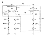
図1乃至図3を参照して、本発明の第1実施形態に係る磁気ランダムアクセスメモリについて説明する。図1は、第1実施形態に係る磁気ランダムアクセスメモリの主要部を概略的に示す回路図である。図1に示すように、メモリセルMCおよび参照セルRCが行列状に配置される。メモリセルMC、直列接続された磁気抵抗効果(MR)素子MRMと選択トランジスタTMとからなる。参照セルRCは、直列接続されたMR素子MRRと選択トランジスタTRとからなる。選択トランジスタTM、TRは、例えば、n型のMOSFET(metal oxide semiconductor field effect transistor)から構成される。
(First embodiment)
A magnetic random access memory according to the first embodiment of the present invention will be described with reference to FIGS. FIG. 1 is a circuit diagram schematically showing a main part of the magnetic random access memory according to the first embodiment. As shown in FIG. 1, memory cells MC and reference cells RC are arranged in a matrix. The memory cell MC includes a magnetoresistive effect (MR) element MRM and a selection transistor TM connected in series. Reference cell RC includes MR element MRR and select transistor TR connected in series. The selection transistors TM and TR are composed of, for example, an n-type MOSFET (metal oxide semiconductor field effect transistor).
MR素子MRM、MRRは、内部の磁化状態に応じた少なくとも2つの定常状態を取り得る。より具体的には、MR素子MRM、MRRは、スピン偏極した電子の電子流(スピン偏極した電流)を、2つの端子の一端から他端、他端から一端に供給されることによって、低抵抗状態または高抵抗状態を取るように構成される。2つの抵抗状態の一方を“0”データ、他方を“1”データに対応させることによって、MR素子MRM、MRRは2値のデータを記憶できる。参照セルRCのMR素子MRRは、メモリセルMCのMR素子MRMと同じ工程で形成され、このため膜厚、材料等は同じである。しかしながら、MR素子MRRは内部の磁化状態が実質的に変化しないように構成される。 The MR elements MRM and MRR can take at least two steady states corresponding to the internal magnetization state. More specifically, the MR elements MRM and MRR are supplied with a spin-polarized electron current (spin-polarized current) from one end of the two terminals to the other end and from the other end to the one end, It is configured to take a low resistance state or a high resistance state. By making one of the two resistance states correspond to “0” data and the other to “1” data, the MR elements MRM and MRR can store binary data. The MR element MRR of the reference cell RC is formed in the same process as the MR element MRM of the memory cell MC, and therefore the film thickness, material, etc. are the same. However, the MR element MRR is configured such that the internal magnetization state does not substantially change.
ここで、MR素子MRM、MRRについて図2を参照して説明する。図2は、MR素子MRM、MRRとして利用可能なMR素子MRの断面図である。MR素子MRは、最も典型的な例として、例えば、図2に示すように、少なくとも、順に積層された、強磁性材料からなる固定層103、非磁性材料からなる中間層102、強磁性材料からなる自由層(記録層)101を含んでいる。
Here, the MR elements MRM and MRR will be described with reference to FIG. FIG. 2 is a cross-sectional view of an MR element MR that can be used as the MR elements MRM and MRR. As the most typical example, for example, as shown in FIG. 2, the MR element MR includes at least a
自由層101および(または)固定層103は、複数のサブレイヤーからなる積層構造とすることも可能である。固定層103の磁化方向は固定される。これは、例えば、固定層103の、非磁性層と反対の面上に反強磁性層104を設けることにより行うことができる。
The
一方、自由層101の磁化方向に関しては、このような固着化機構を設けない。よって、自由層101の磁化方向は可変である。自由層101の磁化容易軸、および固定層103の磁化方向は、自由層101、中間層102、固定層103が相互に面する面に沿った方向を向いている。すなわち、MR素子MRは、いわゆる面内磁化を有する。
On the other hand, no such fixing mechanism is provided for the magnetization direction of the
中間層102として非磁性金属、非磁性半導体、絶縁膜等を用いることができる。
As the
さらに、自由層101の非磁性層102と反対の面上、反強磁性層104の固定層103と反対の面上には、それぞれ、電極105、106が設けられていても良い。
Furthermore,
固定層103の磁化方向に反平行な方向を向いた自由層101の磁化を反転させて、固定層103の磁化方向に平行な方向に向けるには、固定層103から自由層101に向けて電子流を流す。逆に、固定層103の磁化方向に平行な方向を向いた自由層101の磁化を反転させて、固定層103の磁化方向に反平行な方向に向けるには、自由層101から固定層103に向けて電子流を流す。
In order to reverse the magnetization of the
自由層101、固定層103に用いる強磁性材料として、例えばCo、Fe、Ni、またはこれらを含む合金を用いることができる。反強磁性層104の材料としては、Fe−Mn、Pt−Mn、Pt−Cr−Mn、Ni−Mn、Pd−Mn、NiO、Fe2O3、磁性半導体などを用いることができる。
As a ferromagnetic material used for the
中間層102として非磁性金属を用いる場合には、Au、Cu、Cr、Zn、Ga、Nb、Mo、Ru、Pd、Ag、Hf、Ta、W、Pt、Biのうちのいずれか、あるいは、これらのいずれか1種以上を含む合金を用いることができる。また、中間層102をトンネルバリア層として機能させる場合には、Al2O3、SiO2、MgO、AlNなどを用いることができる。
When a nonmagnetic metal is used for the
なお、MR素子MRは、図2に示すものの上下が反転した形であっても良い。また、自由層101、固定層103の磁化は、MR素子MRの各層を貫く方向に沿っていてもよい。すなわち、MR素子MRが、いわゆる垂直磁化を有していてもよい。
Note that the MR element MR may have a vertically inverted shape as shown in FIG. Further, the magnetizations of the
MRAMは、任意の1つのメモリセルMCのMR素子(セル用MR素子)MRMに、セル用MR素子MRMを低抵抗状態に設定する方向の電流と、高抵抗状態に設定する方向の電流とを供給することが可能に構成される。このような電流を流すことは、様々な構成によって実現可能であり、この構成によって本発明は限定されない。以下に、一例について説明する。 In the MRAM, an MR element (cell MR element) MRM of any one memory cell MC is supplied with a current in a direction for setting the cell MR element MRM in a low resistance state and a current in a direction for setting the high resistance state. It is configured to be able to supply. Flowing such a current can be realized by various configurations, and the present invention is not limited by these configurations. Below, an example is demonstrated.
例えば、図1に示すように、任意の列(図1では例として第3列)が、参照セルRC用に割り当てられる。参照セルRCのMR素子MRRの自由層101は、磁化が反転しないように構成されており、例えば固定される。
For example, as shown in FIG. 1, an arbitrary column (third column as an example in FIG. 1) is allocated for the reference cell RC. The
メモリセルMC、参照セルRCの各一端(例えばMR素子側)は、それぞれビット線BM1、BR1と接続される。各ビット線BM1、BR1は、それぞれ、スイッチ回路SM1、SR1を介して周辺回路P1と接続される。周辺回路P1は、書き込み回路WCを含んでいる。 One end (for example, the MR element side) of the memory cell MC and the reference cell RC is connected to the bit lines BM1 and BR1, respectively. Each bit line BM1, BR1 is connected to the peripheral circuit P1 via the switch circuits SM1, SR1, respectively. The peripheral circuit P1 includes a write circuit WC.
メモリセルMC、参照セルRCの各他端(例えば選択トランジスタ側)は、それぞれビット線BM2、BR2と接続される。各ビット線BM2、BR2は、それぞれ、スイッチ回路SM2、SR2を介して周辺回路P2と接続される。周辺回路P2は、書き込み回路WC、読み出し回路RCを含んでいる。 The other ends (for example, the selection transistor side) of the memory cell MC and the reference cell RC are connected to the bit lines BM2 and BR2, respectively. Each bit line BM2, BR2 is connected to the peripheral circuit P2 via the switch circuits SM2, SR2, respectively. The peripheral circuit P2 includes a write circuit WC and a read circuit RC.
スイッチ回路SM1、SM2アクセス対象のメモリセルMCを特定するアドレス信号に応じた信号に従ってオン、オフする。また、スイッチ回路SR1、SR2は、読み出し時にオンされる。スイッチ回路SM1、SM2、SR1、SR2は、例えば、MOSFETによって構成される。そして、周辺回路P1、P2は、アクセス対象のメモリセルMCと接続されたビット線BM1、BM2と接続されたスイッチ回路SM1、SM2がオンとされることにより、アクセス対象のメモリセルMCと電気的に接続される。 The switch circuits SM1 and SM2 are turned on and off according to a signal corresponding to an address signal that specifies the memory cell MC to be accessed. The switch circuits SR1 and SR2 are turned on at the time of reading. The switch circuits SM1, SM2, SR1, SR2 are configured by, for example, MOSFETs. The peripheral circuits P1 and P2 are electrically connected to the memory cell MC to be accessed by turning on the switch circuits SM1 and SM2 connected to the bit lines BM1 and BM2 connected to the memory cell MC to be accessed. Connected to.
書き込み回路WCは、電流ソース/シンク回路を含んでいる。電流ソース/シンク回路は、接続されたビット線BM1、BM2に電流を供給する機能と、接続されたビット線BM1、BM2から電流を引き抜く機能とを有する。 The write circuit WC includes a current source / sink circuit. The current source / sink circuit has a function of supplying current to the connected bit lines BM1 and BM2, and a function of drawing current from the connected bit lines BM1 and BM2.
第n(nは自然数)行目の選択トランジスタTM、TRのゲート端子(電極)はワード線WLnと接続される。ワード線WLnは、ロウデコーダRDと接続される。ロウデコーダRDは、MRAMの外部から供給されたアドレス信号によって指定されるワード線WLnを活性化する。 The gate terminals (electrodes) of the selection transistors TM and TR in the n-th (n is a natural number) row are connected to the word line WLn. Word line WLn is connected to row decoder RD. The row decoder RD activates a word line WLn specified by an address signal supplied from the outside of the MRAM.
読み出し回路RCは、後に詳述するように、読み出し電流を供給するための回路、センスアンプ等を含んでいる。読み出し電流の供給回路は、読み出し時に、セル用MR素子MRMが、その磁化の状態に応じて保持するデータを検出することが可能な程度の大きさの電流をMR素子MRMに供給する。センスアンプは、セル用MR素子MRMに電流を供給して抵抗状態を判定する。読み出し回路RCの具体的な構成および動作については後に詳述する。 As will be described in detail later, the read circuit RC includes a circuit for supplying a read current, a sense amplifier, and the like. The read current supply circuit supplies, to the MR element MRM, a current having a magnitude that allows the cell MR element MRM to detect data held in accordance with the magnetization state. The sense amplifier supplies a current to the cell MR element MRM to determine the resistance state. A specific configuration and operation of the read circuit RC will be described in detail later.
図1の例では、書き込み回路WCが、メモリセルアレイの両端にそれぞれ配置される。しかしながら、この例に限られず、上記のように任意のメモリセルMCに双方向の電流を流すことが可能な構成であれば、書き込み回路WCはどのように実現されても構わない。例えば、1対の書き込み回路WCが、共にメモリセルアレイの上側または下側に配置されていても良い。 In the example of FIG. 1, the write circuits WC are arranged at both ends of the memory cell array. However, the present invention is not limited to this example, and the write circuit WC may be realized in any way as long as it is configured to allow bidirectional current to flow to an arbitrary memory cell MC as described above. For example, the pair of write circuits WC may be arranged on the upper side or the lower side of the memory cell array.
同様に、図1の例では、読み出し回路RCは、ビット線BM2、BR2の上端に接続されているが、この接続に限られない。セル用MR素子MRMに読み出し電流を流して、抵抗状態を判定することが可能な配置であれば、任意の形態で実現可能である。例えば、ビット線BM2、BR2の下端と接続されていても良いし、ビット線BM1、BR1と接続されていても良い。 Similarly, in the example of FIG. 1, the read circuit RC is connected to the upper ends of the bit lines BM2 and BR2, but the connection is not limited to this. Any arrangement that can determine the resistance state by supplying a read current to the cell MR element MRM can be realized. For example, it may be connected to the lower ends of the bit lines BM2 and BR2, or may be connected to the bit lines BM1 and BR1.
あるメモリセルMCにデータを書き込む際、この書き込み対象のメモリセルMC内の選択トランジスタTMがオンされ、この書き込み対象のメモリセルMCを含むメモリセル列のビット線BM1、BM2と接続されたスイッチ回路SM1、SM2がオンとされる。そして、2つの書き込み回路WCのうちの書き込みデータに応じた一方が電流ソース回路として機能し、他方が電流シンク回路として機能する。この結果、書き込み電流が、書き込み回路WC相互間を、スイッチ回路SM1、ビット線BM1、書き込み対象のメモリセルMC、ビット線BM2、スイッチ回路SM2を介して流れる。 When data is written in a certain memory cell MC, the selection transistor TM in the memory cell MC to be written is turned on, and the switch circuit connected to the bit lines BM1 and BM2 of the memory cell column including the memory cell MC to be written SM1 and SM2 are turned on. One of the two write circuits WC corresponding to the write data functions as a current source circuit, and the other functions as a current sink circuit. As a result, the write current flows between the write circuits WC via the switch circuit SM1, the bit line BM1, the write target memory cell MC, the bit line BM2, and the switch circuit SM2.
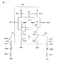
次に、図3を参照して、読み出し回路およびその動作について説明する。図3は、第1実施形態の読み出しに関する回路の構成を示している。より具体的には、図3は、ある1つのメモリセルMCについての読み出しに関与する要素を抽出して示しており、このメモリセルMCの読み出し時に用いられる1つの参照セルRCが共に示されている。なお、図3に関する選択トランジスタTM、TRは、読み出し時にはオンされるので、省略されている。 Next, the read circuit and its operation will be described with reference to FIG. FIG. 3 shows a circuit configuration relating to reading in the first embodiment. More specifically, FIG. 3 shows extracted elements involved in reading for one memory cell MC, and shows one reference cell RC used for reading the memory cell MC together. Yes. Note that the selection transistors TM and TR related to FIG. 3 are omitted because they are turned on at the time of reading.
図3に示すように、読み出し回路RCは、センスアンプSA、クランプ用のn型MOSFET Qn1、Qn2、Vref生成回路REFを含んでいる。Vref生成回路REFは、定電流回路I、クランプ用のn型MOSFET Qn3、スイッチ回路S1、S2、レプリカ抵抗MRP1を含んでいる。Vref生成回路REFは、参照用MR素子MRRに供給される参照電流の値を制御する。 As shown in FIG. 3, the read circuit RC includes a sense amplifier SA, clamping n-type MOSFETs Qn1, Qn2, and a Vref generation circuit REF. The Vref generation circuit REF includes a constant current circuit I, an n-type MOSFET Qn3 for clamping, switch circuits S1 and S2, and a replica resistor MRP1. The Vref generation circuit REF controls the value of the reference current supplied to the reference MR element MRR.
読み出し対象のメモリセルのMR素子MRMの一端は、スイッチ回路SM1を介して共通電位(接地電位)端と接続される。また、セル用MR素子MRMの他端は、スイッチ回路SM2を介してトランジスタQn1の一端と接続される。トランジスタQn1の他端は、センスアンプSAの第1入力端IN1と接続される。トランジスタQn1のゲート端子には、一定の電位Vclmpが印加される。トランジスタQn1は、ゲート端子の電圧によってソース端子の電圧を(ゲート電圧−閾値電圧)近傍に調整する機能を有する。セル用MR素子MRMに印加されるバイアス電圧は電位Vclmpの値によって決定される。 One end of the MR element MRM of the memory cell to be read is connected to the common potential (ground potential) end via the switch circuit SM1. The other end of the cell MR element MRM is connected to one end of the transistor Qn1 via the switch circuit SM2. The other end of the transistor Qn1 is connected to the first input terminal IN1 of the sense amplifier SA. A constant potential Vclmp is applied to the gate terminal of the transistor Qn1. The transistor Qn1 has a function of adjusting the voltage of the source terminal close to (gate voltage−threshold voltage) by the voltage of the gate terminal. The bias voltage applied to the cell MR element MRM is determined by the value of the potential Vclmp.
参照用メモリセルのMR素子MRRの一端は、スイッチ回路SR1を介して共通電位端と接続される。また、参照用MR素子MRRの他端は、スイッチ回路SR2を介してトランジスタQn2の一端と接続される。トランジスタQn2の他端は、センスアンプSAの第2入力端子IN2と接続される。トランジスタQn2は、ゲート端子の電圧によってソース端子の電圧を(ゲート電圧−閾値電圧)近傍に調整する機能を有する。センスアンプSAは、第1入力端子IN1を流れる読み出し電流Ireadと、第2入力端子IN2を流れる参照電流Irefとの比較の結果得られる電位差を増幅する。 One end of the MR element MRR of the reference memory cell is connected to the common potential end via the switch circuit SR1. The other end of the reference MR element MRR is connected to one end of the transistor Qn2 via the switch circuit SR2. The other end of the transistor Qn2 is connected to the second input terminal IN2 of the sense amplifier SA. The transistor Qn2 has a function of adjusting the voltage of the source terminal close to (gate voltage−threshold voltage) by the voltage of the gate terminal. The sense amplifier SA amplifies the potential difference obtained as a result of the comparison between the read current Iread flowing through the first input terminal IN1 and the reference current Iref flowing through the second input terminal IN2.
参照用MR素子MRRの抵抗状態(自由層の磁化方向と固定層の磁化方向との関係)は低抵抗状態か高抵抗状態のどちらか一方に固定される。例えば、読み出し電流IreadがMR素子MRMを低抵抗状態へと変化させる方向に流れるように設定されている場合、参照用MR素子MRRを低抵抗状態に固定しておくことができる。これにより、参照電流Irefによって参照用MR素子MRRが高抵抗状態へと誤って反転することを防止できる。参照用MR素子MRRを流れる参照電流Irefは、読み出し電流Ireadと通常同じ方向に流れ、この方向の参照電流Irefによって参照用MR素子MRRが取る抵抗状態に固定されることになるからである。 The resistance state (relation between the magnetization direction of the free layer and the magnetization direction of the fixed layer) of the reference MR element MRR is fixed to either the low resistance state or the high resistance state. For example, when the read current Iread is set to flow in a direction that changes the MR element MRM to the low resistance state, the reference MR element MRR can be fixed in the low resistance state. Thereby, it is possible to prevent the reference MR element MRR from being erroneously inverted to the high resistance state by the reference current Iref. This is because the reference current Iref flowing through the reference MR element MRR normally flows in the same direction as the read current Iread, and is fixed to the resistance state taken by the reference MR element MRR by the reference current Iref in this direction.
センスアンプSAに入力される参照電流Irefは、参照用MR素子MRRを用いて生成される。そして、参照用MR素子MRRは、セル用MRMと同じ特性を有する。このため、センスアンプSAの第1、第2入力端子IN1、IN2は、同様の充電特性(同様のRC特性)を有する。逆に、参照電流Irefの生成にMR素子を使わないと、第1、第2入力端子IN1、IN2の充電時間に差が出る。これにより、センスアンプSAの高速動作が妨げられる。使用形態の要請からそれほどの高速動作が求められない、例えばNOR型フラッシュメモリ等においては、センスアンプの入力端子の充電特性の大きな差は、それほど問題ではない。しかしながら、MRAMのような、非常に高い速度での動作が求められる装置では、わずかな充電時間の違いも問題になる。そこで、上記のように、第1、第2入力端子IN1、IN2の充電特性を近くすることによって、センスアンプSAの高速動作が可能となる。 The reference current Iref input to the sense amplifier SA is generated using the reference MR element MRR. The reference MR element MRR has the same characteristics as the cell MRM. For this reason, the first and second input terminals IN1 and IN2 of the sense amplifier SA have similar charging characteristics (similar RC characteristics). Conversely, if the MR element is not used to generate the reference current Iref, there will be a difference in the charging time of the first and second input terminals IN1 and IN2. This hinders the high speed operation of the sense amplifier SA. For example, in a NOR flash memory or the like where a high speed operation is not required due to a request for a usage pattern, a large difference in charging characteristics of the input terminal of the sense amplifier is not so problematic. However, in a device such as MRAM that requires operation at a very high speed, a slight difference in charging time also becomes a problem. Therefore, as described above, the sense amplifier SA can be operated at high speed by making the charging characteristics of the first and second input terminals IN1 and IN2 close to each other.
定電流回路Iは、所定の値の参照電流Irefを出力する。参照電流Irefは、低抵抗状態のセル用MR素子MRMを流れる電流の値と高抵抗状態のセル用MR素子MRMを流れる電流の値との中間の値を有する。定電流回路Iは、トランジスタQn3の一端と接続される。トランジスタQn3の一端はまた、自身のゲート端子と接続される。 The constant current circuit I outputs a reference current Iref having a predetermined value. The reference current Iref has an intermediate value between the value of the current flowing through the cell MR element MRM in the low resistance state and the value of the current flowing through the cell MR element MRM in the high resistance state. Constant current circuit I is connected to one end of transistor Qn3. One end of the transistor Qn3 is also connected to its gate terminal.
トランジスタQn3は、トランジスタQn2と同じサイズ(ひいては同じ電流駆動能力)を有する。トランジスタQn3の他端は、スイッチ回路S1の一端と接続される。スイッチ回路S1は、例えばMOSFETから構成することができる。 The transistor Qn3 has the same size (as a result, the same current driving capability) as the transistor Qn2. The other end of the transistor Qn3 is connected to one end of the switch circuit S1. The switch circuit S1 can be composed of, for example, a MOSFET.
スイッチ回路S1の他端は、レプリカ抵抗素子MRP1の一端と接続される。レプリカ抵抗素子MRP1の他端は、スイッチ回路S2を介して共通電位端と接続される。スイッチ回路S2は、例えばMOSFETから構成することができる。 The other end of the switch circuit S1 is connected to one end of the replica resistance element MRP1. The other end of the replica resistance element MRP1 is connected to the common potential end via the switch circuit S2. The switch circuit S2 can be composed of, for example, a MOSFET.
レプリカ抵抗素子MRP1は、参照用MR素子MRRと同じ抵抗値を有する。この目的を達成するために、例えば、レプリカ抵抗素子MRP1は、MR素子から構成され、その抵抗状態を固定される。この例においては、レプリカMR素子MRP1は、レプリカMR素子MRP1を流れる参照電流Irefによって参照用MR素子MRRが取る抵抗状態に固定されることが好ましい。こうすることにより、定電流回路Iからの出力電流によって、レプリカMR素子MRP1への誤書込みが生じることを防止できる。例えば、レプリカ抵抗素子MRRは、低抵抗状態に固定される。 The replica resistance element MRP1 has the same resistance value as that of the reference MR element MRR. In order to achieve this object, for example, the replica resistance element MRP1 is composed of an MR element, and its resistance state is fixed. In this example, replica MR element MRP1 is preferably fixed in a resistance state taken by reference MR element MRR by reference current Iref flowing through replica MR element MRP1. By doing so, it is possible to prevent erroneous writing to the replica MR element MRP1 due to the output current from the constant current circuit I. For example, replica resistance element MRR is fixed in a low resistance state.
より具体的には、レプリカMR素子MRP1は、セル用MR素子MRM、参照用MR素子MRRと同じ特性を有し、参照用MR素子MRRと同じ抵抗状態に固定することができる。レプリカMR素子MRP1は、例えばセル用MR素子MRMや、参照用MR素子MRRと同じ工程で同時に同じ材料から作成され、さらに同じ形状、膜厚に作成され、例えば図2の構成を有する。よって、セル用MR素子MRMおよび参照用MR素子MRRと、レプリカMR素子MRPとは、原理的には同じ特性を有する。すなわち、製造工程上のばらつき等に起因する特性の差を考慮しなければ、2つのMR素子の、低抵抗状態および高抵抗状態における抵抗値は同じである。特性のばらつきを考慮しても、実質的に同じ抵抗値が発現する。 More specifically, replica MR element MRP1 has the same characteristics as cell MR element MRM and reference MR element MRR, and can be fixed in the same resistance state as reference MR element MRR. The replica MR element MRP1 is formed from the same material at the same time in the same process as, for example, the cell MR element MRM and the reference MR element MRR, and is formed to have the same shape and film thickness. Therefore, the cell MR element MRM, the reference MR element MRR, and the replica MR element MRP have the same characteristics in principle. In other words, the resistance values in the low resistance state and the high resistance state of the two MR elements are the same unless the difference in characteristics due to variations in the manufacturing process is taken into consideration. Even when variation in characteristics is taken into consideration, substantially the same resistance value appears.
トランジスタQn2のゲート端子は、トランジスタQn3のゲート端子の電位Vrefと同じ電位となるように、直接、または回路を介して間接的に接続される。図3では、トランジスタQn2のゲート端子とトランジスタQn3のゲート端子とは、直接、接続される。 The gate terminal of the transistor Qn2 is connected directly or indirectly through a circuit so as to have the same potential as the potential Vref of the gate terminal of the transistor Qn3. In FIG. 3, the gate terminal of the transistor Qn2 and the gate terminal of the transistor Qn3 are directly connected.
上記のように、トランジスタQn2、Qn3はサイズが同じであり、これらトランジスタQn2、Qn3の各ゲート端子には同じ電位Vrefが印加され、これらトランジスタQn2、Qn3の各ソース端子には同じ抵抗値を有する素子MRR、MRP1がそれぞれ接続される。このため、Vref生成回路REFは電流転送回路として機能し、センスアンプSAの第2入力端子IN2には、定電流回路Iが出力する参照電流Irefと同じ値の電流が流れる。 As described above, the transistors Qn2 and Qn3 have the same size, the same potential Vref is applied to the gate terminals of the transistors Qn2 and Qn3, and the source terminals of the transistors Qn2 and Qn3 have the same resistance value. Elements MRR and MRP1 are connected to each other. Therefore, the Vref generation circuit REF functions as a current transfer circuit, and a current having the same value as the reference current Iref output from the constant current circuit I flows through the second input terminal IN2 of the sense amplifier SA.
なお、Vref生成回路REFは、1つのMRAMチップに対して1つ設けられる。そして、1つのMRAMチップにおいて、複数の読み出し回路RCが設けられ、これら読み出し回路RCが、1つのVref生成回路REFを共用する。したがって、1つのトランジスタQn3のゲート端子が、複数のトランジスタQn2の各ゲート端子と接続される。そして、トランジスタQn2のゲート端子とトランジスタQn3のゲート端子とが直接接続される。直接接続されるため、何らかの回路を介して接続する場合と異なり、トランジスタQn2のゲート端子の電位とトランジスタQn3のゲート端子の電位とにばらつきが生じない。このため、複数のトランジスタQn2の各ゲート端子相互間の電位のばらつきも小さく、動作特性が均一になる利点を得られる。 One Vref generation circuit REF is provided for one MRAM chip. A plurality of read circuits RC are provided in one MRAM chip, and these read circuits RC share one Vref generation circuit REF. Therefore, the gate terminal of one transistor Qn3 is connected to each gate terminal of a plurality of transistors Qn2. The gate terminal of the transistor Qn2 and the gate terminal of the transistor Qn3 are directly connected. Since they are directly connected, unlike the case of connection via some circuit, there is no variation in the potential of the gate terminal of the transistor Qn2 and the potential of the gate terminal of the transistor Qn3. For this reason, the variation in potential between the gate terminals of the plurality of transistors Qn2 is small, and an advantage of uniform operating characteristics can be obtained.
一方、トランジスタQn3のゲート端子が、複数のトランジスタQn2の各ゲート端子と接続されるため、トランジスタQn2のゲート端子の電位の充電に時間を要する。しかしながら、この充電は、MRAMの電源投入時に行われ、その後の読み出し動作ごとに行なわれるわけではない。このため、充電に時間がかかるとしても、大きな問題は生じない。 On the other hand, since the gate terminal of the transistor Qn3 is connected to each gate terminal of the plurality of transistors Qn2, it takes time to charge the potential of the gate terminal of the transistor Qn2. However, this charging is performed when the power of the MRAM is turned on, and is not performed for each subsequent read operation. For this reason, even if charging takes time, a big problem does not arise.
以上述べたように、第1実施形態に係る磁気ランダムアクセスメモリによれば、参照用MR素子MRRと接続されるトランジスタQn2のゲート端子には、トランジスタQn2と同じサイズを有し且つ参照用MR素子MRRと同じ抵抗値を有するレプリカMR素子MRP1と接続されたトランジスタQn3のゲート端子およびソース端子の電位が印加される。このため、トランジスタQn3を流れる参照電流Irefと同じ値の電流を、トランジスタQn2と接続されたセンスアンプSAの入力端子に供給することができる。そして、このような動作を、オペアンプを用いずに簡単な回路で実現できるので、読み出し回路RCの面積の削減と読み出し動作時の消費電力の抑制とを達成できる。 As described above, according to the magnetic random access memory according to the first embodiment, the gate terminal of the transistor Qn2 connected to the reference MR element MRR has the same size as the transistor Qn2 and the reference MR element. The potentials of the gate terminal and the source terminal of transistor Qn3 connected to replica MR element MRP1 having the same resistance value as MRR are applied. Therefore, a current having the same value as the reference current Iref flowing through the transistor Qn3 can be supplied to the input terminal of the sense amplifier SA connected to the transistor Qn2. Since such an operation can be realized with a simple circuit without using an operational amplifier, it is possible to reduce the area of the readout circuit RC and suppress the power consumption during the readout operation.
(第2実施形態)
第2実施形態は、トランジスタQn2とトランジスタQn3との接続の仕方に関する。図4は、本発明の第2実施形態に係る磁気ランダムアクセスメモリの主要部を概略的に示す回路図である。図4に示すように、読み出し回路RCにおいて、トランジスタQn3のゲート端子の電位は、ユニティゲインバッファを介して、トランジスタQn2のゲート端子に転送される。
(Second Embodiment)
The second embodiment relates to how to connect the transistor Qn2 and the transistor Qn3. FIG. 4 is a circuit diagram schematically showing main parts of a magnetic random access memory according to the second embodiment of the present invention. As shown in FIG. 4, in the read circuit RC, the potential of the gate terminal of the transistor Qn3 is transferred to the gate terminal of the transistor Qn2 via the unity gain buffer.
具体的には、トランジスタQn3のゲート端子は、オペアンプOPの非反転入力端子と接続される。また、オペアンプOPの出力端子は、オペアンプOPの反転入力端子と接続されるとともに、トランジスタQn2のゲート端子と接続される。トランジスタQn2とトランジスタQN3とをこのように接続しても、トランジスタQn2のゲート端子とトランジスタQn3のゲート端子とを同じ電位とすることができる。その他の構成については、第1実施形態と同じである。 Specifically, the gate terminal of the transistor Qn3 is connected to the non-inverting input terminal of the operational amplifier OP. The output terminal of the operational amplifier OP is connected to the inverting input terminal of the operational amplifier OP and to the gate terminal of the transistor Qn2. Even if the transistors Qn2 and QN3 are connected in this way, the gate terminal of the transistor Qn2 and the gate terminal of the transistor Qn3 can be set to the same potential. About another structure, it is the same as 1st Embodiment.
トランジスタQn2のゲート端子とトランジスタQN3のゲート端子とをオペアンプOPを介して接続すれば、トランジスタQn2のゲート端子の充電を、第1実施形態よりも速く行なうことができる。よって、第2実施形態は、読み出し回路RCが多い場合、したがってトランジスタQn2の数が多い場合に有効である。 If the gate terminal of the transistor Qn2 and the gate terminal of the transistor QN3 are connected via the operational amplifier OP, the gate terminal of the transistor Qn2 can be charged faster than in the first embodiment. Therefore, the second embodiment is effective when the number of readout circuits RC is large, and therefore when the number of transistors Qn2 is large.
本発明の第2実施形態に係る磁気ランダムアクセスメモリによれば、第1実施形態と同じくVref生成回路REFを用いて、定電流回路Iが出力する参照電流IrefがセンスアンプSAの第2入力端子IN2に供給される。このため、第1実施形態と同じ効果を得られる。 According to the magnetic random access memory according to the second embodiment of the present invention, the reference current Iref output from the constant current circuit I is the second input terminal of the sense amplifier SA using the Vref generation circuit REF as in the first embodiment. Supplied to IN2. For this reason, the same effect as the first embodiment can be obtained.
また、第2実施形態によれば、トランジスタQn3のゲート端子の電位は、オペアンプOPを用いて、トランジスタQn2のゲート端子に転送される。このため、トランジスタQn2のゲート端子の充電時間を短くできる。 Further, according to the second embodiment, the potential of the gate terminal of the transistor Qn3 is transferred to the gate terminal of the transistor Qn2 using the operational amplifier OP. For this reason, the charging time of the gate terminal of the transistor Qn2 can be shortened.
(第3実施形態)
第3実施形態は、第1、第2実施形態の定電流回路Iの具体例に関する。
(Third embodiment)
The third embodiment relates to a specific example of the constant current circuit I of the first and second embodiments.
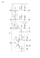
図5は、本発明の第3実施形態に係る磁気ランダムアクセスメモリの読み出し回路RCの主要部を概略的に示す回路図である。定電流回路Iは、図5に示す構成を有する。 FIG. 5 is a circuit diagram schematically showing a main part of the read circuit RC of the magnetic random access memory according to the third embodiment of the present invention. The constant current circuit I has a configuration shown in FIG.
図5に示すように、定電流回路Iにおいて、p型MOSFET Qp1、n型MOSFET Qn11、レプリカMR素子MRP2が直列接続される。そして、この直列接続構造が、電源電位端と共通電位端との間に接続される。トランジスタQp1のゲート端子は、トランジスタQp1のドレイン端子と接続される。トランジスタQn11のゲート端子にはクランプ電位Vclmpが供給される。 As shown in FIG. 5, in the constant current circuit I, a p-type MOSFET Qp1, an n-type MOSFET Qn11, and a replica MR element MRP2 are connected in series. The series connection structure is connected between the power supply potential end and the common potential end. The gate terminal of transistor Qp1 is connected to the drain terminal of transistor Qp1. The clamp potential Vclmp is supplied to the gate terminal of the transistor Qn11.
また、定電流回路Iにおいて、p型MOSFET Qp2、n型MOSFET Qn13、レプリカMR素子MRP3が直列接続される。そして、この直列接続構造が、電源電位端と共通電位(接地電位)端との間に接続される。トランジスタQp2のゲート端子は、トランジスタQp1のゲート端子およびトランジスタQp2のドレイン端子と接続される。トランジスタQn13のゲート端子にはクランプ電位Vclmpが供給される。 In the constant current circuit I, a p-type MOSFET Qp2, an n-type MOSFET Qn13, and a replica MR element MRP3 are connected in series. This series connection structure is connected between the power supply potential end and the common potential (ground potential) end. The gate terminal of transistor Qp2 is connected to the gate terminal of transistor Qp1 and the drain terminal of transistor Qp2. A clamp potential Vclmp is supplied to the gate terminal of the transistor Qn13.
トランジスタQp1、Qp2のゲート端子は、p型MOSFET Qp3のゲート端子と接続される。トランジスタQp3の一端は、電源電位端と接続され、他端は定電流回路Iの出力端として機能するとともにトランジスタQn3の一端と接続される。 The gate terminals of the transistors Qp1 and Qp2 are connected to the gate terminal of the p-type MOSFET Qp3. One end of the transistor Qp3 is connected to the power supply potential end, and the other end functions as an output end of the constant current circuit I and is connected to one end of the transistor Qn3.
レプリカMR素子MRP2、MRP3は、セル用MR素子MRMと、原理的には同じ特性を有する。すなわち、製造工程上のばらつき等に起因する特性の差を考慮しなければ、レプリカMR素子MRP2、MRP3の低抵抗状態および高抵抗状態における抵抗値は、セル用MR素子MRMと同じである。特性のばらつきを考慮しても、実質的に同じ抵抗値が発現する。そして、レプリカMR素子MRP2、MRP3の各抵抗状態の一方が高抵抗状態に固定され、他方が低抵抗状態に固定される。 The replica MR elements MRP2 and MRP3 have the same characteristics in principle as the cell MR element MRM. That is, unless the difference in characteristics caused by variations in the manufacturing process is considered, the resistance values of the replica MR elements MRP2 and MRP3 in the low resistance state and the high resistance state are the same as those of the cell MR element MRM. Even when variation in characteristics is taken into consideration, substantially the same resistance value appears. One of the resistance states of replica MR elements MRP2 and MRP3 is fixed to the high resistance state, and the other is fixed to the low resistance state.
Vref生成回路REFは、スイッチ回路S1とレプリカMR素子MRP1との間にn型MOSFET Qn4が接続されることを除いて、第1実施形態(図3)と同じである。トランジスタQn4のゲート端子には、電源電位Vddが供給される。 The Vref generation circuit REF is the same as that in the first embodiment (FIG. 3) except that an n-type MOSFET Qn4 is connected between the switch circuit S1 and the replica MR element MRP1. The power supply potential Vdd is supplied to the gate terminal of the transistor Qn4.
これ以外の構成については、第1実施形態と同じである。なお、図5において、スイッチ回路SM1、SM2、SR1、SR2、S1、S2は、オンしている状態を示しているものとして省略されている。 Other configurations are the same as those in the first embodiment. In FIG. 5, the switch circuits SM1, SM2, SR1, SR2, S1, and S2 are omitted because they indicate the ON state.
なお、Vref生成回路REFの出力を第2実施形態のように、ユニティゲインバッファを介してトランジスタQn2のゲート端子に供給することももちろん可能である。この構成によれば、第2実施形態で述べた効果を得ることができる。 Of course, it is also possible to supply the output of the Vref generation circuit REF to the gate terminal of the transistor Qn2 via the unity gain buffer as in the second embodiment. According to this configuration, the effects described in the second embodiment can be obtained.
定電流回路Iは上記のような構成を有し、且つレプリカMR素子MRP2、MRP3は、一方が低抵抗状態、他方が高抵抗状態に固定される。このため、定電流回路Iの出力である参照電流Irefは、低抵抗状態のレプリカセル用MR素子を流れる電流と、高抵抗状態のレプリカセル用MR素子を流れる電流との平均値に等しい。なお、この平均値は、低抵抗状態のメモリセル用MR素子MRMを流れる電流の値と、高抵抗状態のメモリセル用MR素子MRMを流れる電流の値との平均の値と実質的に同じである。レプリカMR素子MRP2、MRP3とメモリセル用MR素子MRMとの特性が、上記のように、実質的に同じだからである。 The constant current circuit I has the above-described configuration, and one of the replica MR elements MRP2 and MRP3 is fixed to a low resistance state and the other is fixed to a high resistance state. Therefore, the reference current Iref, which is the output of the constant current circuit I, is equal to the average value of the current flowing through the replica cell MR element in the low resistance state and the current flowing through the replica cell MR element in the high resistance state. The average value is substantially the same as the average value of the current flowing through the memory cell MR element MRM in the low resistance state and the current flowing through the memory cell MR element MRM in the high resistance state. is there. This is because the characteristics of the replica MR elements MRP2, MRP3 and the MR element MRM for memory cells are substantially the same as described above.
第3実施形態に係る磁気ランダムアクセスメモリによれば、それぞれ高抵抗状態および低抵抗状態のレプリカMR素子MRP2、MRP3を用いて生成された参照電流Irefが、第1実施形態と同じくVref生成回路REFを用いてセンスアンプSAの第2入力端子IN2に転送される。このため、低抵抗状態のセル用MR素子MRMを流れる電流値と高抵抗状態のセル用MR素子MRMを流れる電流値との間の値を有する参照電流Irefを、簡便な回路を用いてセンスアンプSAに供給することができる。よって、読み出し回路の面積の削減と読み出し動作時の消費電力の抑制とを達成できる。 According to the magnetic random access memory according to the third embodiment, the reference current Iref generated using the replica MR elements MRP2 and MRP3 in the high resistance state and the low resistance state, respectively, is the Vref generation circuit REF as in the first embodiment. Is transferred to the second input terminal IN2 of the sense amplifier SA. Therefore, a reference current Iref having a value between a current value flowing through the low-resistance cell MR element MRM and a current value flowing through the high-resistance cell MR element MRM is detected using a simple circuit. SA can be supplied. Therefore, it is possible to reduce the area of the reading circuit and suppress the power consumption during the reading operation.
(第4実施形態)
第4実施形態は、第1、第2実施形態の定電流回路Iの具体例に関する。
(Fourth embodiment)
The fourth embodiment relates to a specific example of the constant current circuit I of the first and second embodiments.
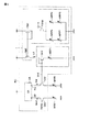
図6は、本発明の第4実施形態に係る磁気ランダムアクセスメモリの読み出し回路RCの主要部を概略的に示す回路図である。定電流回路Iは、図6に示す構成を有する。 FIG. 6 is a circuit diagram schematically showing the main part of the read circuit RC of the magnetic random access memory according to the fourth embodiment of the present invention. The constant current circuit I has a configuration shown in FIG.
図6に示すように、定電流回路Iにおいて、p型MOSFET Qp4、n型MOSFET Qn15、2つのレプリカMR素子MRP4、MRP5が直列接続される。そして、この直列接続構造が、電源電位端と共通電位端との間に接続される。また、レプリカMR素子MRP4、MRP5と並列に、直列接続された2つのレプリカMR素子MRP6、MRP7が接続される。 As shown in FIG. 6, in the constant current circuit I, a p-type MOSFET Qp4, an n-type MOSFET Qn15, and two replica MR elements MRP4 and MRP5 are connected in series. The series connection structure is connected between the power supply potential end and the common potential end. Further, two replica MR elements MRP6 and MRP7 connected in series are connected in parallel with the replica MR elements MRP4 and MRP5.
トランジスタQp4のゲート端子は、トランジスタQp4のドレイン端子およびトランジスタQp3のゲート端子と接続される。トランジスタQn15のゲート端子にはクランプ電位Vclmpが供給される。 The gate terminal of transistor Qp4 is connected to the drain terminal of transistor Qp4 and the gate terminal of transistor Qp3. A clamp potential Vclmp is supplied to the gate terminal of the transistor Qn15.
レプリカMR素子MRP4、MRP5、MRP6、MRP7は、メモリセル用MR素子MRMと、原理的には同じ特性を有する。すなわち、製造工程上のばらつき等に起因する特性の差を考慮しなければ、レプリカMR素子MRP4乃至MRP7の低抵抗状態および高抵抗状態における抵抗値は、セル用MR素子MRMと同じである。特性のばらつきを考慮しても、実質的に同じ抵抗値が発現する。レプリカMR素子MRP4、MRP5は、高抵抗状態に固定され、レプリカMR素子MRP6、MRP7は、低抵抗状態に固定される。 Replica MR elements MRP4, MRP5, MRP6, and MRP7 have the same characteristics in principle as MR elements MRM for memory cells. That is, unless the difference in characteristics caused by variations in the manufacturing process is taken into consideration, the resistance values of the replica MR elements MRP4 to MRP7 in the low resistance state and the high resistance state are the same as those of the cell MR element MRM. Even when variation in characteristics is taken into consideration, substantially the same resistance value appears. Replica MR elements MRP4 and MRP5 are fixed in a high resistance state, and replica MR elements MRP6 and MRP7 are fixed in a low resistance state.
Vref生成回路REFの構成は、第3実施形態と同じである。また、上記した構成以外の構成については、第1実施形態と同じである。なお、図6において、スイッチ回路SM1、SM2、SR1、SR2、S1、S2は、オンしている状態を示すものとして省略されている。 The configuration of the Vref generation circuit REF is the same as that of the third embodiment. The configuration other than the above configuration is the same as that of the first embodiment. In FIG. 6, the switch circuits SM1, SM2, SR1, SR2, S1, and S2 are omitted to show the on state.
なお、Vref生成回路REFの出力Vrefを第2実施形態のように、ユニティゲインバッファを介してトランジスタQn2のゲート端子に供給することももちろん可能である。この構成によれば、第2実施形態で述べた効果を得ることができる。 Of course, the output Vref of the Vref generation circuit REF can be supplied to the gate terminal of the transistor Qn2 via the unity gain buffer as in the second embodiment. According to this configuration, the effects described in the second embodiment can be obtained.
定電流回路Iは上記のような構成を有し、且つレプリカMR素子MRP4、MRP5は高抵抗状態に固定され、レプリカMR素子MRP6、MRP7は低抵抗状態に固定される。このため、定電流回路Iの出力である参照電流Irefは、低抵抗状態のレプリカセル用MR素子を流れる電流と、高抵抗状態のレプリカセル用MR素子を流れる電流との平均値に等しい。なお、この平均値は、低抵抗状態のセル用MR素子MRを流れる電流の値と、高抵抗状態のセル用MR素子MRMを流れる電流の値との平均の値と実質的に同じである。レプリカMR素子MRP4乃至MRP7とセル用MR素子MRMとの特性が、上記のように、実質的に同じだからである。 The constant current circuit I has the above-described configuration, and the replica MR elements MRP4 and MRP5 are fixed in a high resistance state, and the replica MR elements MRP6 and MRP7 are fixed in a low resistance state. Therefore, the reference current Iref, which is the output of the constant current circuit I, is equal to the average value of the current flowing through the replica cell MR element in the low resistance state and the current flowing through the replica cell MR element in the high resistance state. This average value is substantially the same as the average value of the current value flowing through the low-resistance cell MR element MR and the current value flowing through the high-resistance cell MR element MRM. This is because the characteristics of the replica MR elements MRP4 to MRP7 and the cell MR element MRM are substantially the same as described above.
第4実施形態に係る磁気ランダムアクセスメモリによれば、それぞれ高抵抗状態のレプリカMR素子MRP4、5および低抵抗状態のレプリカMR素子MRP6、MRP7を用いて生成された参照電流Irefが、第1実施形態と同じくVref生成回路REFを用いてセンスアンプSAの第2入力端子IN2に転送される。このため、低抵抗状態のMR素子を流れる電流値と高抵抗状態のMR素子を流れる電流値との間の値を有する参照電流Irefを、簡便な回路を用いてセンスアンプSAに供給することができる。よって、読み出し回路の面積の削減と読み出し動作時の消費電力の抑制とを達成できる。 According to the magnetic random access memory according to the fourth embodiment, the reference current Iref generated using the replica MR elements MRP4 and 5 in the high resistance state and the replica MR elements MRP6 and MRP7 in the low resistance state are the first embodiment. Similarly to the embodiment, the signal is transferred to the second input terminal IN2 of the sense amplifier SA using the Vref generation circuit REF. Therefore, the reference current Iref having a value between the current value flowing through the MR element in the low resistance state and the current value flowing through the MR element in the high resistance state can be supplied to the sense amplifier SA using a simple circuit. it can. Therefore, it is possible to reduce the area of the reading circuit and suppress the power consumption during the reading operation.
また、第4実施形態によれば、直列接続された高抵抗状態のレプリカMR素子MRP4、MRP5と、直列接続された低抵抗状態のレプリカMR素子MRP6、MRP7と、の並列構造を用いて参照電流Irefが生成される。このため、スタンバイ時の電流を抑制することができる。 Further, according to the fourth embodiment, the reference current is configured using a parallel structure of the series-connected high-resistance state replica MR elements MRP4 and MRP5 and the series-connected low-resistance state replica MR elements MRP6 and MRP7. Iref is generated. For this reason, the current at the time of standby can be suppressed.
(第5実施形態)
第5実施形態は、第1乃至第4実施形態のセンスアンプSAの具体例に関する。
(Fifth embodiment)
The fifth embodiment relates to a specific example of the sense amplifier SA of the first to fourth embodiments.
図7は、本発明の第5実施形態に係る磁気ランダムアクセスメモリのセンスアンプSAの主要部を概略的に示す回路図である。図7に示すように、p型MOSFET Qp11、Qp12の各一端は、電源電位端と接続される。トランジスタQp11、Qp12の各ゲート端子同士は、相互に接続されるとともにp型MOSFET Qp13のゲート端子と接続される。トランジスタQp13のゲート端子には、また、制御信号SE1が供給される。トランジスタQp13の一端は、トランジスタQP11の他端と接続されるとともに、センスアンプSAの第1出力端OUTとして機能する。トランジスタQp13の他端は、トランジスタQP12の他端と接続されるとともに、センスアンプSAの第2出力端/OUTとして機能する。第1出力端OUTの電位と第2出力端/OUTとの電位は、相補の関係を有する。 FIG. 7 is a circuit diagram schematically showing the main part of the sense amplifier SA of the magnetic random access memory according to the fifth embodiment of the present invention. As shown in FIG. 7, one end of each of the p-type MOSFETs Qp11 and Qp12 is connected to a power supply potential end. The gate terminals of the transistors Qp11 and Qp12 are connected to each other and to the gate terminal of the p-type MOSFET Qp13. A control signal SE1 is also supplied to the gate terminal of the transistor Qp13. One end of the transistor Qp13 is connected to the other end of the transistor QP11 and functions as the first output terminal OUT of the sense amplifier SA. The other end of the transistor Qp13 is connected to the other end of the transistor QP12 and functions as the second output terminal / OUT of the sense amplifier SA. The potential of the first output terminal OUT and the potential of the second output terminal / OUT have a complementary relationship.
電源電位端と共通電位端との間には、直列接続されたp型MOSFET Qp14、2つのn型MOSFET Qn21、Qn22が接続される。トランジスタQp14、Qn21の各ゲート端子は相互に接続されるとともに、第2出力端/OUTと接続される。トランジスタQp14とトランジスタQn21との接続ノードは、第1出力端OUTと接続される。 A p-type MOSFET Qp14 and two n-type MOSFETs Qn21 and Qn22 connected in series are connected between the power supply potential end and the common potential end. The gate terminals of the transistors Qp14 and Qn21 are connected to each other and to the second output terminal / OUT. A connection node between the transistor Qp14 and the transistor Qn21 is connected to the first output terminal OUT.
電源電位端と共通電位端との間には、直列接続されたp型MOSFET Qp15、2つのn型MOSFET Qn23、Qn24が接続される。トランジスタQp15、Qn23の各ゲート端子は相互に接続されるとともに、第1出力端OUTと接続される。トランジスタQp15とトランジスタQn23との接続ノードは、第2出力端/OUTと接続される。トランジスタQn24のゲート端子は、トランジスタQn22のゲート端子と接続されるとともに、制御信号SE2を供給される。 A p-type MOSFET Qp15 and two n-type MOSFETs Qn23 and Qn24 connected in series are connected between the power supply potential end and the common potential end. The gate terminals of the transistors Qp15 and Qn23 are connected to each other and to the first output terminal OUT. A connection node between the transistor Qp15 and the transistor Qn23 is connected to the second output terminal / OUT. The gate terminal of the transistor Qn24 is connected to the gate terminal of the transistor Qn22 and is supplied with a control signal SE2.
トランジスタQn21とトランジスタQn22との接続ノードは、第1入力端IN1として機能する。第1入力端IN1は、トランジスタQn1と接続される。トランジスタQn23とトランジスタQn24との接続ノードは、第2入力端IN2として機能する。第2入力端IN2は、トランジスタQn2と接続される。 A connection node between the transistor Qn21 and the transistor Qn22 functions as the first input terminal IN1. The first input terminal IN1 is connected to the transistor Qn1. A connection node between the transistor Qn23 and the transistor Qn24 functions as the second input terminal IN2. The second input terminal IN2 is connected to the transistor Qn2.
第5実施形態に係るセンスアンプSAは、電流差動増幅型であり、以下に述べるように動作する。まず、動作に先立ち、第1、第2出力端OUT、/OUTが電源電位Vddへとプリチャージされる。そして、スイッチ回路SM1、SM2、SR1、SR2をオンすることによって、センスアンプSAにセル電流、参照電流が供給される。次に、制御信号SE1をローレベルとすることによってセンス動作が開始する。この結果、第1、第2出力端OUT、/OUTに、メモリセルの保持データに応じた電位が現れる。そして、適当な時間の経過後、制御信号SE2をハイレベルにすることによって、第1、第2出力端OUT、/OUTの電位が確定する。 The sense amplifier SA according to the fifth embodiment is a current differential amplification type, and operates as described below. First, prior to the operation, the first and second output terminals OUT and / OUT are precharged to the power supply potential Vdd. Then, by turning on the switch circuits SM1, SM2, SR1, and SR2, a cell current and a reference current are supplied to the sense amplifier SA. Next, the sensing operation is started by setting the control signal SE1 to the low level. As a result, a potential corresponding to the data held in the memory cell appears at the first and second output terminals OUT and / OUT. Then, after an appropriate time has elapsed, the potential of the first and second output terminals OUT and / OUT is determined by setting the control signal SE2 to a high level.
その他、本発明の思想の範疇において、当業者であれば、各種の変更例及び修正例に想到し得るものであり、それら変更例及び修正例についても本発明の範囲に属するものと了解される。 In addition, in the category of the idea of the present invention, those skilled in the art can conceive of various changes and modifications, and it is understood that these changes and modifications also belong to the scope of the present invention. .
MRM…セル用MR素子、MRR…参照用MR素子、SM1、SM2、SR1、SR2、S1、S2…スイッチ回路、RC…読み出し回路、SA…センスアンプ、Qn1、Qn2、Qn3…MOSFET、I…定電流回路、S1、S2…スイッチ回路、MRP1…レプリカMR素子。 MRM: MR element for cell, MRR: MR element for reference, SM1, SM2, SR1, SR2, S1, S2 ... Switch circuit, RC ... Read circuit, SA ... Sense amplifier, Qn1, Qn2, Qn3 ... MOSFET, I ... Constant Current circuit, S1, S2 ... switch circuit, MRP1 ... replica MR element.
Claims (5)
低抵抗状態と前記低抵抗状態よりも高い抵抗値を有する高抵抗状態との2つの定常状態のいずれか一方に固定された第2磁気抵抗効果素子と、
一端を前記第1磁気抵抗効果素子と接続され、ゲート端子に第1電位を印加された第1MOSFETと、
一端を前記第2磁気抵抗効果素子と接続された第2MOSFETと、
前記第1MOSFETの他端を流れる電流と前記第2MOSFETの他端を流れる電流との差を増幅するセンスアンプと、
低抵抗状態の前記第1磁気抵抗効果素子を流れる電流と、高抵抗状態の前記第1磁気抵抗効果素子を流れる電流と、の間の値を有する参照電流を出力する定電流回路と、
一端において前記参照電流を供給され、前記一端と接続されたゲート端子を有する第3MOSFETと、
前記第3MOSFETの他端と接続され、前記第2磁気抵抗効果素子と実質的に同じ抵抗値を有する第1抵抗素子と、
を具備し、
前記第2MOSFETのゲート端子には、前記第3MOSFETのゲート端子と同じ電位が印加される、
ことを特徴とする磁気ランダムアクセスメモリ。 A first magnetoresistive element having two steady states, a low resistance state and a high resistance state having a higher resistance value than the low resistance state;
A second magnetoresistive element fixed to one of two steady states of a low resistance state and a high resistance state having a higher resistance value than the low resistance state;
A first MOSFET having one end connected to the first magnetoresistive element and a first potential applied to a gate terminal;
A second MOSFET having one end connected to the second magnetoresistive element;
A sense amplifier that amplifies a difference between a current flowing through the other end of the first MOSFET and a current flowing through the other end of the second MOSFET;
A constant current circuit that outputs a reference current having a value between a current flowing through the first magnetoresistive effect element in a low resistance state and a current flowing through the first magnetoresistive effect element in a high resistance state;
A third MOSFET which is supplied with the reference current at one end and has a gate terminal connected to the one end;
A first resistive element connected to the other end of the third MOSFET and having substantially the same resistance value as the second magnetoresistive element;
Comprising
The same potential as that of the gate terminal of the third MOSFET is applied to the gate terminal of the second MOSFET.
Magnetic random access memory characterized by that.
一端を電源電位端と接続され、他端を自身のゲート端子および前記第3MOSFETの前記一端と接続された第4MOSFETと、
一端を前記電源電位端と接続され、他端を自身のゲート端子および前記第4MOSFETの前記ゲート端子と接続された第5MOSFETと、
一端を前記電源電位端と接続され、他端を自身のゲート端子および前記第4MOSFETの前記ゲート端子と接続された第6MOSFETと、
一端を前記第5MOSFETの前記他端と接続され、他端を前記第2抵抗素子と接続され、ゲート端子に前記第1電位を印加される第7MOSFETと、
一端を前記第6MOSFETの前記他端と接続され、他端を前記第3抵抗素子と接続され、ゲート端子に前記第1電位を印加される第8MOSFETと、
をさらに含むことを特徴とする請求項3に記載の磁気ランダムアクセスメモリ。 The constant current circuit is:
A fourth MOSFET having one end connected to the power supply potential end and the other end connected to its gate terminal and the one end of the third MOSFET;
A fifth MOSFET having one end connected to the power supply potential end and the other end connected to its own gate terminal and the gate terminal of the fourth MOSFET;
A sixth MOSFET having one end connected to the power supply potential end and the other end connected to its own gate terminal and the gate terminal of the fourth MOSFET;
A seventh MOSFET having one end connected to the other end of the fifth MOSFET, the other end connected to the second resistance element, and the first potential applied to a gate terminal;
An eighth MOSFET having one end connected to the other end of the sixth MOSFET, the other end connected to the third resistance element, and the gate terminal applied with the first potential;
The magnetic random access memory according to claim 3, further comprising:
前記第2磁気抵抗効果素子および前記第1乃至第3抵抗素子は、前記第1磁性膜と同じ特性を有する第3強磁性膜と、前記第2強磁性膜と同じ特性を有する第4協磁性膜と、前記第1非磁性膜と同じ特性を有し且つ前記第3、第4強磁性膜間に設けられた第2非磁性膜と、を含み、且つ抵抗状態を固定されている、
ことを特徴とする請求項3に記載の磁気ランダムアクセスメモリ。 The first magnetoresistive element includes a first ferromagnetic film, a second ferromagnetic film, and a first nonmagnetic film provided between the first and second ferromagnetic films,
The second magnetoresistance effect element and the first to third resistance elements are a third ferromagnetic film having the same characteristics as the first magnetic film, and a fourth cooperative magnetism having the same characteristics as the second ferromagnetic film. Including a film and a second nonmagnetic film having the same characteristics as the first nonmagnetic film and provided between the third and fourth ferromagnetic films, and having a fixed resistance state.
The magnetic random access memory according to claim 3.
Priority Applications (2)
| Application Number | Priority Date | Filing Date | Title |
|---|---|---|---|
| JP2007175564A JP4896830B2 (en) | 2007-07-03 | 2007-07-03 | Magnetic random access memory |
| US12/164,410 US7791930B2 (en) | 2007-07-03 | 2008-06-30 | Magnetoresistive random access memory |
Applications Claiming Priority (1)
| Application Number | Priority Date | Filing Date | Title |
|---|---|---|---|
| JP2007175564A JP4896830B2 (en) | 2007-07-03 | 2007-07-03 | Magnetic random access memory |
Publications (2)
| Publication Number | Publication Date |
|---|---|
| JP2009015949A JP2009015949A (en) | 2009-01-22 |
| JP4896830B2 true JP4896830B2 (en) | 2012-03-14 |
Family
ID=40221289
Family Applications (1)
| Application Number | Title | Priority Date | Filing Date |
|---|---|---|---|
| JP2007175564A Expired - Fee Related JP4896830B2 (en) | 2007-07-03 | 2007-07-03 | Magnetic random access memory |
Country Status (2)
| Country | Link |
|---|---|
| US (1) | US7791930B2 (en) |
| JP (1) | JP4896830B2 (en) |
Families Citing this family (22)
| Publication number | Priority date | Publication date | Assignee | Title |
|---|---|---|---|---|
| JP5002401B2 (en) * | 2007-10-03 | 2012-08-15 | 株式会社東芝 | Resistance change memory |
| JP2010079974A (en) * | 2008-09-25 | 2010-04-08 | Toshiba Corp | Semiconductor memory device |
| JP2011003241A (en) * | 2009-06-18 | 2011-01-06 | Toshiba Corp | Semiconductor memory |
| US8213213B2 (en) * | 2009-11-09 | 2012-07-03 | National Tsing Hua University | Reference current generator for resistance type memory and method thereof |
| US8254195B2 (en) * | 2010-06-01 | 2012-08-28 | Qualcomm Incorporated | High-speed sensing for resistive memories |
| US8693273B2 (en) * | 2012-01-06 | 2014-04-08 | Headway Technologies, Inc. | Reference averaging for MRAM sense amplifiers |
| US9111622B2 (en) * | 2012-05-09 | 2015-08-18 | Everspin Technologies, Inc. | Self referencing sense amplifier for spin torque MRAM |
| US9183912B2 (en) | 2012-05-17 | 2015-11-10 | Everspin Technologies, Inc. | Circuit and method for controlling MRAM cell bias voltages |
| CN104956481B (en) * | 2013-02-19 | 2018-01-09 | 松下知识产权经营株式会社 | Nonvolatile semiconductor memory device |
| US8947920B2 (en) | 2013-03-22 | 2015-02-03 | Masahiro Takahashi | Memory device |
| US9177641B2 (en) | 2013-03-22 | 2015-11-03 | Masahiro Takahashi | Memory device |
| US9070440B2 (en) | 2013-08-26 | 2015-06-30 | Masahiro Takahashi | Resistance change memory |
| WO2015132980A1 (en) * | 2014-03-07 | 2015-09-11 | Akira Katayama | Memory device |
| US10043564B2 (en) | 2014-12-10 | 2018-08-07 | Toshiba Memory Corporation | Semiconductor memory device and method of controlling semiconductor memory device |
| US9502106B2 (en) | 2014-12-10 | 2016-11-22 | Kabushiki Kaisha Toshiba | Semiconductor memory device and method of controlling semiconductor memory device |
| US9747966B2 (en) * | 2015-08-25 | 2017-08-29 | Toshiba Memory Corporation | Semiconductor memory device for sensing memory cell with variable resistance |
| US9679643B1 (en) * | 2016-03-09 | 2017-06-13 | Taiwan Semiconductor Manufacturing Co., Ltd. | Resistive memory device having a trimmable resistance of at least on of a driver and a sinker is trimmed based on a row location |
| JP6574862B1 (en) * | 2018-03-15 | 2019-09-11 | 株式会社東芝 | Memory device |
| US10839879B2 (en) * | 2018-09-27 | 2020-11-17 | Taiwan Semiconductor Manufacturing Co., Ltd. | Read techniques for a magnetic tunnel junction (MTJ) memory device with a current mirror |
| US10803913B1 (en) * | 2019-06-11 | 2020-10-13 | Applied Materials, Inc. | Narrow range sense amplifier with immunity to noise and variation |
| US10796741B1 (en) * | 2019-10-30 | 2020-10-06 | Nxp Usa, Inc. | Non-volatile memory with a select gate regulator circuit |
| DE102020109378A1 (en) | 2020-04-03 | 2021-10-07 | Infineon Technologies Ag | Read circuit for resistive change memory |
Family Cites Families (9)
| Publication number | Priority date | Publication date | Assignee | Title |
|---|---|---|---|---|
| US5608676A (en) * | 1993-08-31 | 1997-03-04 | Crystal Semiconductor Corporation | Current limited current reference for non-volatile memory sensing |
| US6385109B1 (en) | 2001-01-30 | 2002-05-07 | Motorola, Inc. | Reference voltage generator for MRAM and method |
| US6944048B2 (en) * | 2001-11-29 | 2005-09-13 | Kabushiki Kaisha Toshiba | Magnetic random access memory |
| JP2003173700A (en) * | 2001-12-03 | 2003-06-20 | Mitsubishi Electric Corp | Semiconductor storage device |
| US6600690B1 (en) * | 2002-06-28 | 2003-07-29 | Motorola, Inc. | Sense amplifier for a memory having at least two distinct resistance states |
| US6700814B1 (en) * | 2002-10-30 | 2004-03-02 | Motorola, Inc. | Sense amplifier bias circuit for a memory having at least two distinct resistance states |
| JP2006210396A (en) * | 2005-01-25 | 2006-08-10 | Fujitsu Ltd | Magnetic memory device and reading method thereof |
| US7313043B2 (en) * | 2005-11-29 | 2007-12-25 | Altis Semiconductor Snc | Magnetic Memory Array |
| US7495971B2 (en) * | 2006-04-19 | 2009-02-24 | Infineon Technologies Ag | Circuit and a method of determining the resistive state of a resistive memory cell |
-
2007
- 2007-07-03 JP JP2007175564A patent/JP4896830B2/en not_active Expired - Fee Related
-
2008
- 2008-06-30 US US12/164,410 patent/US7791930B2/en active Active
Also Published As
| Publication number | Publication date |
|---|---|
| US7791930B2 (en) | 2010-09-07 |
| US20090010045A1 (en) | 2009-01-08 |
| JP2009015949A (en) | 2009-01-22 |
Similar Documents
| Publication | Publication Date | Title |
|---|---|---|
| JP4896830B2 (en) | Magnetic random access memory | |
| JP4768770B2 (en) | Semiconductor memory device | |
| Chen et al. | A 130 nm 1.2 V/3.3 V 16 Kb spin-transfer torque random access memory with nondestructive self-reference sensing scheme | |
| JP5422665B2 (en) | Spin torque bit cell with unfixed reference layer and unidirectional write current | |
| US7760543B2 (en) | Resistance change memory | |
| US6930911B2 (en) | Magnetic memory device, method for writing on the same and method for reading from the same | |
| CN111755050A (en) | non-volatile memory device | |
| US7511992B2 (en) | Magnetic memory device | |
| US20080175044A1 (en) | Magnetic memory cell and magnetic memory device | |
| EP3945521A1 (en) | Magnetic random access memory cell and method for reading said cell | |
| CN108630262A (en) | Semiconductor storage | |
| US20070291531A1 (en) | Mram with a write driver and a method therefor | |
| JP4283011B2 (en) | Magnetic memory device and reading method thereof | |
| CN111128265B (en) | Magnetic tunnel junction reading circuit, device and method for reading magnetic tunnel junction | |
| JP4361067B2 (en) | MRAM memory cell | |
| CN108182957B (en) | A kind of MRAM readout circuit using reference voltage | |
| US8514614B2 (en) | Magnetic memory | |
| CN106796815B (en) | Nonvolatile semiconductor memory | |
| TWI537947B (en) | Magnetoresistive memory device | |
| CN109935273B (en) | Circuit for screening MTJ (magnetic tunnel junction) resistance | |
| JP3808835B2 (en) | Signal transmission system between semiconductor devices | |
| JP2011198416A (en) | Magnetic memory | |
| JP2003085968A (en) | Readout circuit of magnetic memory device | |
| JP4741758B2 (en) | Read circuit of magnetic memory device | |
| JP2012256388A (en) | Semiconductor device |
Legal Events
| Date | Code | Title | Description |
|---|---|---|---|
| A621 | Written request for application examination |
Free format text: JAPANESE INTERMEDIATE CODE: A621 Effective date: 20090806 |
|
| A977 | Report on retrieval |
Free format text: JAPANESE INTERMEDIATE CODE: A971007 Effective date: 20111109 |
|
| TRDD | Decision of grant or rejection written | ||
| A01 | Written decision to grant a patent or to grant a registration (utility model) |
Free format text: JAPANESE INTERMEDIATE CODE: A01 Effective date: 20111129 |
|
| A01 | Written decision to grant a patent or to grant a registration (utility model) |
Free format text: JAPANESE INTERMEDIATE CODE: A01 |
|
| A61 | First payment of annual fees (during grant procedure) |
Free format text: JAPANESE INTERMEDIATE CODE: A61 Effective date: 20111221 |
|
| FPAY | Renewal fee payment (event date is renewal date of database) |
Free format text: PAYMENT UNTIL: 20150106 Year of fee payment: 3 |
|
| LAPS | Cancellation because of no payment of annual fees |