JP4895936B2 - 導電性ボールの搭載方法 - Google Patents
導電性ボールの搭載方法 Download PDFInfo
- Publication number
- JP4895936B2 JP4895936B2 JP2007188630A JP2007188630A JP4895936B2 JP 4895936 B2 JP4895936 B2 JP 4895936B2 JP 2007188630 A JP2007188630 A JP 2007188630A JP 2007188630 A JP2007188630 A JP 2007188630A JP 4895936 B2 JP4895936 B2 JP 4895936B2
- Authority
- JP
- Japan
- Prior art keywords
- conductive ball
- flux
- paste
- receiving port
- conductive
- Prior art date
- Legal status (The legal status is an assumption and is not a legal conclusion. Google has not performed a legal analysis and makes no representation as to the accuracy of the status listed.)
- Expired - Fee Related
Links
Images


Classifications
-
- B—PERFORMING OPERATIONS; TRANSPORTING
- B23—MACHINE TOOLS; METAL-WORKING NOT OTHERWISE PROVIDED FOR
- B23K—SOLDERING OR UNSOLDERING; WELDING; CLADDING OR PLATING BY SOLDERING OR WELDING; CUTTING BY APPLYING HEAT LOCALLY, e.g. FLAME CUTTING; WORKING BY LASER BEAM
- B23K1/00—Soldering, e.g. brazing, or unsoldering
- B23K1/0008—Soldering, e.g. brazing, or unsoldering specially adapted for particular articles or work
- B23K1/0016—Brazing of electronic components
-
- B—PERFORMING OPERATIONS; TRANSPORTING
- B23—MACHINE TOOLS; METAL-WORKING NOT OTHERWISE PROVIDED FOR
- B23K—SOLDERING OR UNSOLDERING; WELDING; CLADDING OR PLATING BY SOLDERING OR WELDING; CUTTING BY APPLYING HEAT LOCALLY, e.g. FLAME CUTTING; WORKING BY LASER BEAM
- B23K3/00—Tools, devices, or special appurtenances for soldering, e.g. brazing, or unsoldering, not specially adapted for particular methods
- B23K3/06—Solder feeding devices; Solder melting pans
- B23K3/0607—Solder feeding devices
- B23K3/0623—Solder feeding devices for shaped solder piece feeding, e.g. preforms, bumps, balls, pellets, droplets
-
- H—ELECTRICITY
- H05—ELECTRIC TECHNIQUES NOT OTHERWISE PROVIDED FOR
- H05K—PRINTED CIRCUITS; CASINGS OR CONSTRUCTIONAL DETAILS OF ELECTRIC APPARATUS; MANUFACTURE OF ASSEMBLAGES OF ELECTRICAL COMPONENTS
- H05K3/00—Apparatus or processes for manufacturing printed circuits
- H05K3/30—Assembling printed circuits with electric components, e.g. with resistor
- H05K3/32—Assembling printed circuits with electric components, e.g. with resistor electrically connecting electric components or wires to printed circuits
- H05K3/34—Assembling printed circuits with electric components, e.g. with resistor electrically connecting electric components or wires to printed circuits by soldering
- H05K3/3457—Solder materials or compositions; Methods of application thereof
- H05K3/3478—Applying solder preforms; Transferring prefabricated solder patterns
-
- H—ELECTRICITY
- H05—ELECTRIC TECHNIQUES NOT OTHERWISE PROVIDED FOR
- H05K—PRINTED CIRCUITS; CASINGS OR CONSTRUCTIONAL DETAILS OF ELECTRIC APPARATUS; MANUFACTURE OF ASSEMBLAGES OF ELECTRICAL COMPONENTS
- H05K2203/00—Indexing scheme relating to apparatus or processes for manufacturing printed circuits covered by H05K3/00
- H05K2203/01—Tools for processing; Objects used during processing
- H05K2203/0104—Tools for processing; Objects used during processing for patterning or coating
- H05K2203/0113—Female die used for patterning or transferring, e.g. temporary substrate having recessed pattern
-
- H—ELECTRICITY
- H05—ELECTRIC TECHNIQUES NOT OTHERWISE PROVIDED FOR
- H05K—PRINTED CIRCUITS; CASINGS OR CONSTRUCTIONAL DETAILS OF ELECTRIC APPARATUS; MANUFACTURE OF ASSEMBLAGES OF ELECTRICAL COMPONENTS
- H05K2203/00—Indexing scheme relating to apparatus or processes for manufacturing printed circuits covered by H05K3/00
- H05K2203/04—Soldering or other types of metallurgic bonding
- H05K2203/041—Solder preforms in the shape of solder balls
-
- H—ELECTRICITY
- H05—ELECTRIC TECHNIQUES NOT OTHERWISE PROVIDED FOR
- H05K—PRINTED CIRCUITS; CASINGS OR CONSTRUCTIONAL DETAILS OF ELECTRIC APPARATUS; MANUFACTURE OF ASSEMBLAGES OF ELECTRICAL COMPONENTS
- H05K2203/00—Indexing scheme relating to apparatus or processes for manufacturing printed circuits covered by H05K3/00
- H05K2203/04—Soldering or other types of metallurgic bonding
- H05K2203/0485—Tacky flux, e.g. for adhering components during mounting
-
- H—ELECTRICITY
- H05—ELECTRIC TECHNIQUES NOT OTHERWISE PROVIDED FOR
- H05K—PRINTED CIRCUITS; CASINGS OR CONSTRUCTIONAL DETAILS OF ELECTRIC APPARATUS; MANUFACTURE OF ASSEMBLAGES OF ELECTRICAL COMPONENTS
- H05K2203/00—Indexing scheme relating to apparatus or processes for manufacturing printed circuits covered by H05K3/00
- H05K2203/07—Treatments involving liquids, e.g. plating, rinsing
- H05K2203/0736—Methods for applying liquids, e.g. spraying
- H05K2203/074—Features related to the fluid pressure
Description
導電性ボールの搭載位置に導電性ボール受容口を有する位置決め層と支持層とが積層して成る導電性ボール仮配置板であって、該支持層は少なくとも該位置決め層の導電性ボール受容口の部位では下記フラックスを透過可能である導電性ボール仮配置板を用い、
導電性ボールをフラックス中に分散させたペーストを、上記導電性ボール仮配置板の位置決め層側から刷り込んで、各導電性ボール受容口内に各1個の導電性ボールを含むペーストを保持させ、
上記導電性ボール仮配置板の導電性ボール受容口を上記基板の接続パッドに位置合わせして、各導電性ボール受容口内に保持されたペーストを各接続パッドに転写することにより、接続パッド上にフラックスを伴った導電性ボールを搭載することを特徴とする導電性ボールの搭載方法が提供される。
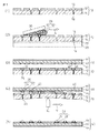
図1に、本発明の一実施形態によるはんだボールの搭載方法を示す。
位置決め層12の厚さ:100μm
支持層14の厚さ:50μm
はんだボール受容口16の開口ピッチ:200μm
位置決め層12は、Ni等のアディティブめっき等により作製することができる。支持層14は、Ni等のアディティブめっき等により作製することができるし、樹脂基板を加工して作製することもできる。
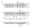
図2に、仮配置板10へのペースト28の刷り込みを、位置決め層12上でのピストン加圧により行なう実施形態を示す。仮配置板10は、実施形態1とは異なり支持層14Xがメッシュから成る。ただし、これは単に一つの選択肢を示したのであって、仮配置板10を特にこの場合にメッシュに限定する必要はなく、実施形態1と同様にメッシュ状ではなく貫通孔18を有する形態でもよい。
図3に、はんだボール仮配置板10のはんだボール受容口16から基板40の接続パッド46へのペースト28の転写を、支持層14の裏面側からのエアーブローによって行なう実施形態を示す。エアブローは、大気や窒素ガス等、何らかの気体の噴射による。実施形態1においては、このペースト28の上記転写を通常のスクリーン印刷における転写方法と同じく、スキージ等の押圧子50により仮配置板10を撓ませることにより行なうので、仮配置板10はそのために十分な可撓性を備えるように、材質や厚さに制限があった。本実施形態の方法によれば、仮配置板10は上記のような可撓性を必要としない。
図4に、仮配置板10をシリコンウェハの加工により一体として作製する例を示す。
12、12S 位置決め層
14、14X、14S 支持層
16、16S はんだボール受容口
18、18S 貫通孔
20 ステージ
22 フラックス吸収シート
24 はんだボール
26 フラックス
28 ペースト
30 スキージ
40 基板
42 多層回路部
44 ソルダーレジスト層
46 接続パッド
48 開口
50 押圧子
52 シリンダ
54 ピストン
56 ピストン軸
60 エアーブローユニット
70 シリコン素板
70’ シリコンウェハ
72 レジストパターン
74 開口
78 レジストパターン
80 開口
Claims (8)
- 基板上の複数の接続パッド上に各1個の導電性ボールを搭載する方法であって、
導電性ボールの搭載位置に導電性ボール受容口を有する位置決め層と支持層とが積層して成る導電性ボール仮配置板であって、該支持層は少なくとも該位置決め層の導電性ボール受容口の部位では下記フラックスを透過可能である導電性ボール仮配置板を用い、
導電性ボールをフラックス中に分散させたペーストを、上記導電性ボール仮配置板の位置決め層側から刷り込んで、各導電性ボール受容口内に各1個の導電性ボールを含むペーストを保持させ、
上記導電性ボール仮配置板の導電性ボール受容口を上記基板の接続パッドに位置合わせして、各導電性ボール受容口内に保持されたペーストを各接続パッドに転写することにより、接続パッド上にフラックスを伴った導電性ボールを搭載することを特徴とする導電性ボールの搭載方法。 - 請求項1において、前記支持層の裏面側に前記フラックスの吸収層を密着配置した状態で、前記位置決め層側から前記ペーストを刷り込むことを特徴とする導電性ボールの搭載方法。
- 請求項1または2において、前記支持層が、前記位置決め層の導電性ボール受容口の部位に、前記フラックスが透過する貫通孔を備えていることを特徴とする導電性ボールの搭載方法。
- 請求項1または2において、前記支持層が、前記フラックスが透過するメッシュから成ることを特徴とする導電性ボールの搭載方法。
- 請求項1から4までのいずれか1項において、前記ペーストの前記導電性ボール仮配置板への刷り込みを、前記位置決め層上でのスキージ操作により行なうことを特徴とする導電性ボールの搭載方法。
- 請求項1から4までのいずれか1項において、前記ペーストの前記導電性ボール仮配置板への刷り込みを、前記位置決め層上でのピストン加圧により行なうことを特徴とする導電性ボールの搭載方法。
- 請求項1から6までのいずれか1項において、前記導電性ボール仮配置板の導電性ボール受容口から前記基板の接続パッドへの前記ペーストの転写を、押圧子による押圧によって行なうことを特徴とする導電性ボールの搭載方法。
- 請求項1から6までのいずれか1項において、前記導電性ボール仮配置板の導電性ボール受容口から前記基板の接続パッドへの前記ペーストの転写を、前記支持層の裏面側からの気体の噴射によって行なうことを特徴とする導電性ボールの搭載方法。
Priority Applications (2)
| Application Number | Priority Date | Filing Date | Title |
|---|---|---|---|
| JP2007188630A JP4895936B2 (ja) | 2007-07-19 | 2007-07-19 | 導電性ボールの搭載方法 |
| US12/173,256 US7820479B2 (en) | 2007-07-19 | 2008-07-15 | Conductive ball mounting method |
Applications Claiming Priority (1)
| Application Number | Priority Date | Filing Date | Title |
|---|---|---|---|
| JP2007188630A JP4895936B2 (ja) | 2007-07-19 | 2007-07-19 | 導電性ボールの搭載方法 |
Publications (3)
| Publication Number | Publication Date |
|---|---|
| JP2009026959A JP2009026959A (ja) | 2009-02-05 |
| JP2009026959A5 JP2009026959A5 (ja) | 2010-06-17 |
| JP4895936B2 true JP4895936B2 (ja) | 2012-03-14 |
Family
ID=40264027
Family Applications (1)
| Application Number | Title | Priority Date | Filing Date |
|---|---|---|---|
| JP2007188630A Expired - Fee Related JP4895936B2 (ja) | 2007-07-19 | 2007-07-19 | 導電性ボールの搭載方法 |
Country Status (2)
| Country | Link |
|---|---|
| US (1) | US7820479B2 (ja) |
| JP (1) | JP4895936B2 (ja) |
Cited By (1)
| Publication number | Priority date | Publication date | Assignee | Title |
|---|---|---|---|---|
| KR20180035676A (ko) * | 2016-09-29 | 2018-04-06 | 신꼬오덴기 고교 가부시키가이샤 | 캐리어 기재 부착 배선 기판 및 캐리어 기재 부착 배선 기판의 제조 방법 |
Families Citing this family (23)
| Publication number | Priority date | Publication date | Assignee | Title |
|---|---|---|---|---|
| US20110017504A1 (en) * | 2009-07-23 | 2011-01-27 | Keith Bryan Hardin | Z-Directed Ferrite Bead Components for Printed Circuit Boards |
| US20110017502A1 (en) * | 2009-07-23 | 2011-01-27 | Keith Bryan Hardin | Z-Directed Components for Printed Circuit Boards |
| US20110017581A1 (en) * | 2009-07-23 | 2011-01-27 | Keith Bryan Hardin | Z-Directed Switch Components for Printed Circuit Boards |
| US8237061B2 (en) * | 2009-07-23 | 2012-08-07 | Lexmark International, Inc. | Z-directed filter components for printed circuit boards |
| US8273996B2 (en) * | 2009-07-23 | 2012-09-25 | Lexmark International, Inc. | Z-directed connector components for printed circuit boards |
| US8198547B2 (en) * | 2009-07-23 | 2012-06-12 | Lexmark International, Inc. | Z-directed pass-through components for printed circuit boards |
| US8278568B2 (en) * | 2009-07-23 | 2012-10-02 | Lexmark International, Inc. | Z-directed variable value components for printed circuit boards |
| US8198548B2 (en) * | 2009-07-23 | 2012-06-12 | Lexmark International, Inc. | Z-directed capacitor components for printed circuit boards |
| US8735734B2 (en) | 2009-07-23 | 2014-05-27 | Lexmark International, Inc. | Z-directed delay line components for printed circuit boards |
| WO2012099602A1 (en) * | 2011-01-21 | 2012-07-26 | Lexmark International, Inc. | Z-directed connector components for printed circuit boards |
| US9009954B2 (en) | 2011-08-31 | 2015-04-21 | Lexmark International, Inc. | Process for manufacturing a Z-directed component for a printed circuit board using a sacrificial constraining material |
| US8943684B2 (en) * | 2011-08-31 | 2015-02-03 | Lexmark International, Inc. | Continuous extrusion process for manufacturing a Z-directed component for a printed circuit board |
| US9078374B2 (en) | 2011-08-31 | 2015-07-07 | Lexmark International, Inc. | Screening process for manufacturing a Z-directed component for a printed circuit board |
| US8752280B2 (en) | 2011-09-30 | 2014-06-17 | Lexmark International, Inc. | Extrusion process for manufacturing a Z-directed component for a printed circuit board |
| US8790520B2 (en) | 2011-08-31 | 2014-07-29 | Lexmark International, Inc. | Die press process for manufacturing a Z-directed component for a printed circuit board |
| US8658245B2 (en) | 2011-08-31 | 2014-02-25 | Lexmark International, Inc. | Spin coat process for manufacturing a Z-directed component for a printed circuit board |
| US8912452B2 (en) | 2012-03-29 | 2014-12-16 | Lexmark International, Inc. | Z-directed printed circuit board components having different dielectric regions |
| US8822838B2 (en) | 2012-03-29 | 2014-09-02 | Lexmark International, Inc. | Z-directed printed circuit board components having conductive channels for reducing radiated emissions |
| US8830692B2 (en) | 2012-03-29 | 2014-09-09 | Lexmark International, Inc. | Ball grid array systems for surface mounting an integrated circuit using a Z-directed printed circuit board component |
| US8822840B2 (en) | 2012-03-29 | 2014-09-02 | Lexmark International, Inc. | Z-directed printed circuit board components having conductive channels for controlling transmission line impedance |
| KR102029077B1 (ko) | 2013-02-04 | 2019-10-07 | 삼성전자주식회사 | 패키지의 외부접속단자 형성 방법 및 이를 수행하기 위한 장치 |
| US9673131B2 (en) * | 2013-04-09 | 2017-06-06 | Intel Corporation | Integrated circuit package assemblies including a glass solder mask layer |
| US9216469B2 (en) * | 2013-10-18 | 2015-12-22 | Taiwan Semiconductor Manufacturing Co., Ltd. | Indirect printing bumping method for solder ball deposition |
Family Cites Families (9)
| Publication number | Priority date | Publication date | Assignee | Title |
|---|---|---|---|---|
| US5284287A (en) * | 1992-08-31 | 1994-02-08 | Motorola, Inc. | Method for attaching conductive balls to a substrate |
| US5431332A (en) * | 1994-02-07 | 1995-07-11 | Motorola, Inc. | Method and apparatus for solder sphere placement using an air knife |
| US5655704A (en) * | 1994-08-30 | 1997-08-12 | Matsushita Electric Industrial Co., Ltd. | Method and apparatus for mounting soldering balls onto electrodes of a substrate or a comparable electronic component |
| CA2135508C (en) * | 1994-11-09 | 1998-11-03 | Robert J. Lyn | Method for forming solder balls on a semiconductor substrate |
| JPH09107045A (ja) | 1995-10-13 | 1997-04-22 | Japan Aviation Electron Ind Ltd | Bgaパッケージのボール取付け方法 |
| JPH10126046A (ja) | 1996-10-18 | 1998-05-15 | Oki Electric Ind Co Ltd | ボール・グリッド・アレイの製造装置 |
| JP2925534B1 (ja) * | 1998-04-28 | 1999-07-28 | 株式会社日鉄マイクロメタル | 金属球配列方法及び配列装置 |
| US6191022B1 (en) * | 1999-04-18 | 2001-02-20 | Cts Corporation | Fine pitch solder sphere placement |
| JP2001320160A (ja) | 2000-05-12 | 2001-11-16 | Fuji Photo Film Co Ltd | クリーム半田塗布方法及び半田供給装置 |
-
2007
- 2007-07-19 JP JP2007188630A patent/JP4895936B2/ja not_active Expired - Fee Related
-
2008
- 2008-07-15 US US12/173,256 patent/US7820479B2/en not_active Expired - Fee Related
Cited By (2)
| Publication number | Priority date | Publication date | Assignee | Title |
|---|---|---|---|---|
| KR20180035676A (ko) * | 2016-09-29 | 2018-04-06 | 신꼬오덴기 고교 가부시키가이샤 | 캐리어 기재 부착 배선 기판 및 캐리어 기재 부착 배선 기판의 제조 방법 |
| KR102394215B1 (ko) * | 2016-09-29 | 2022-05-09 | 신꼬오덴기 고교 가부시키가이샤 | 캐리어 기재 부착 배선 기판 및 캐리어 기재 부착 배선 기판의 제조 방법 |
Also Published As
| Publication number | Publication date |
|---|---|
| US20090020591A1 (en) | 2009-01-22 |
| JP2009026959A (ja) | 2009-02-05 |
| US7820479B2 (en) | 2010-10-26 |
Similar Documents
| Publication | Publication Date | Title |
|---|---|---|
| JP4895936B2 (ja) | 導電性ボールの搭載方法 | |
| US7784671B2 (en) | Apparatus and method for arranging magnetic solder balls | |
| TWI345436B (ja) | ||
| US6316289B1 (en) | Method of forming fine-pitch interconnections employing a standoff mask | |
| JP3056192B1 (ja) | 電極パッド上にバンプを形成したソルダーレジスト層付実装基板の製造方法 | |
| JP4503053B2 (ja) | 導電性ボールの搭載装置および搭載方法 | |
| WO2009144846A1 (ja) | 半田ボール搭載方法 | |
| KR20120108952A (ko) | 회로 기판의 제조 방법 및 전자 장치의 제조 방법 | |
| US6303881B1 (en) | Via connector and method of making same | |
| US6722275B2 (en) | Reservoir stencil with relief areas and method of using | |
| US6569248B1 (en) | Apparatus for selectively applying solder mask | |
| CN113939900A (zh) | 配线基板的制造方法 | |
| JP4118286B2 (ja) | 半田ボール搭載方法 | |
| JP2006261187A (ja) | 部品内蔵基板の製造方法 | |
| JP2003264255A (ja) | 配線基板の製造方法 | |
| KR100754086B1 (ko) | 프로브 카드 및 그 제조방법 | |
| KR100855822B1 (ko) | 기판 인쇄 장치 및 방법 | |
| JP2000307221A (ja) | 電子部品の電気接続方法 | |
| JP2007253593A (ja) | スクリーン印刷方法 | |
| JP2018202774A (ja) | ペースト埋め込み印刷装置 | |
| KR20040110565A (ko) | 메탈 마스크 및 그 제조 방법과 이를 이용하여 다층인쇄회로기판을 제조하는 방법 | |
| JP5067107B2 (ja) | 回路基板および半導体装置 | |
| KR100842255B1 (ko) | 마스크 및 그 제조방법 | |
| JP2006319255A (ja) | 多層配線基板の製造方法 | |
| JPH10321678A (ja) | 導電粒子配列方法及び導電粒子配列テープ |
Legal Events
| Date | Code | Title | Description |
|---|---|---|---|
| A521 | Request for written amendment filed |
Free format text: JAPANESE INTERMEDIATE CODE: A523 Effective date: 20100428 |
|
| A621 | Written request for application examination |
Free format text: JAPANESE INTERMEDIATE CODE: A621 Effective date: 20100428 |
|
| A977 | Report on retrieval |
Free format text: JAPANESE INTERMEDIATE CODE: A971007 Effective date: 20111115 |
|
| TRDD | Decision of grant or rejection written | ||
| A01 | Written decision to grant a patent or to grant a registration (utility model) |
Free format text: JAPANESE INTERMEDIATE CODE: A01 Effective date: 20111122 |
|
| A01 | Written decision to grant a patent or to grant a registration (utility model) |
Free format text: JAPANESE INTERMEDIATE CODE: A01 |
|
| A61 | First payment of annual fees (during grant procedure) |
Free format text: JAPANESE INTERMEDIATE CODE: A61 Effective date: 20111220 |
|
| R150 | Certificate of patent or registration of utility model |
Free format text: JAPANESE INTERMEDIATE CODE: R150 |
|
| FPAY | Renewal fee payment (event date is renewal date of database) |
Free format text: PAYMENT UNTIL: 20150106 Year of fee payment: 3 |
|
| LAPS | Cancellation because of no payment of annual fees |