JP4895936B2 - Mounting method of conductive balls - Google Patents
Mounting method of conductive balls Download PDFInfo
- Publication number
- JP4895936B2 JP4895936B2 JP2007188630A JP2007188630A JP4895936B2 JP 4895936 B2 JP4895936 B2 JP 4895936B2 JP 2007188630 A JP2007188630 A JP 2007188630A JP 2007188630 A JP2007188630 A JP 2007188630A JP 4895936 B2 JP4895936 B2 JP 4895936B2
- Authority
- JP
- Japan
- Prior art keywords
- conductive ball
- flux
- paste
- receiving port
- conductive
- Prior art date
- Legal status (The legal status is an assumption and is not a legal conclusion. Google has not performed a legal analysis and makes no representation as to the accuracy of the status listed.)
- Expired - Fee Related
Links
Images


Classifications
-
- B—PERFORMING OPERATIONS; TRANSPORTING
- B23—MACHINE TOOLS; METAL-WORKING NOT OTHERWISE PROVIDED FOR
- B23K—SOLDERING OR UNSOLDERING; WELDING; CLADDING OR PLATING BY SOLDERING OR WELDING; CUTTING BY APPLYING HEAT LOCALLY, e.g. FLAME CUTTING; WORKING BY LASER BEAM
- B23K1/00—Soldering, e.g. brazing, or unsoldering
- B23K1/0008—Soldering, e.g. brazing, or unsoldering specially adapted for particular articles or work
- B23K1/0016—Brazing of electronic components
-
- B—PERFORMING OPERATIONS; TRANSPORTING
- B23—MACHINE TOOLS; METAL-WORKING NOT OTHERWISE PROVIDED FOR
- B23K—SOLDERING OR UNSOLDERING; WELDING; CLADDING OR PLATING BY SOLDERING OR WELDING; CUTTING BY APPLYING HEAT LOCALLY, e.g. FLAME CUTTING; WORKING BY LASER BEAM
- B23K3/00—Tools, devices, or special appurtenances for soldering, e.g. brazing, or unsoldering, not specially adapted for particular methods
- B23K3/06—Solder feeding devices; Solder melting pans
- B23K3/0607—Solder feeding devices
- B23K3/0623—Solder feeding devices for shaped solder piece feeding, e.g. preforms, bumps, balls, pellets, droplets
-
- H—ELECTRICITY
- H05—ELECTRIC TECHNIQUES NOT OTHERWISE PROVIDED FOR
- H05K—PRINTED CIRCUITS; CASINGS OR CONSTRUCTIONAL DETAILS OF ELECTRIC APPARATUS; MANUFACTURE OF ASSEMBLAGES OF ELECTRICAL COMPONENTS
- H05K3/00—Apparatus or processes for manufacturing printed circuits
- H05K3/30—Assembling printed circuits with electric components, e.g. with resistor
- H05K3/32—Assembling printed circuits with electric components, e.g. with resistor electrically connecting electric components or wires to printed circuits
- H05K3/34—Assembling printed circuits with electric components, e.g. with resistor electrically connecting electric components or wires to printed circuits by soldering
- H05K3/3457—Solder materials or compositions; Methods of application thereof
- H05K3/3478—Applying solder preforms; Transferring prefabricated solder patterns
-
- H—ELECTRICITY
- H05—ELECTRIC TECHNIQUES NOT OTHERWISE PROVIDED FOR
- H05K—PRINTED CIRCUITS; CASINGS OR CONSTRUCTIONAL DETAILS OF ELECTRIC APPARATUS; MANUFACTURE OF ASSEMBLAGES OF ELECTRICAL COMPONENTS
- H05K2203/00—Indexing scheme relating to apparatus or processes for manufacturing printed circuits covered by H05K3/00
- H05K2203/01—Tools for processing; Objects used during processing
- H05K2203/0104—Tools for processing; Objects used during processing for patterning or coating
- H05K2203/0113—Female die used for patterning or transferring, e.g. temporary substrate having recessed pattern
-
- H—ELECTRICITY
- H05—ELECTRIC TECHNIQUES NOT OTHERWISE PROVIDED FOR
- H05K—PRINTED CIRCUITS; CASINGS OR CONSTRUCTIONAL DETAILS OF ELECTRIC APPARATUS; MANUFACTURE OF ASSEMBLAGES OF ELECTRICAL COMPONENTS
- H05K2203/00—Indexing scheme relating to apparatus or processes for manufacturing printed circuits covered by H05K3/00
- H05K2203/04—Soldering or other types of metallurgic bonding
- H05K2203/041—Solder preforms in the shape of solder balls
-
- H—ELECTRICITY
- H05—ELECTRIC TECHNIQUES NOT OTHERWISE PROVIDED FOR
- H05K—PRINTED CIRCUITS; CASINGS OR CONSTRUCTIONAL DETAILS OF ELECTRIC APPARATUS; MANUFACTURE OF ASSEMBLAGES OF ELECTRICAL COMPONENTS
- H05K2203/00—Indexing scheme relating to apparatus or processes for manufacturing printed circuits covered by H05K3/00
- H05K2203/04—Soldering or other types of metallurgic bonding
- H05K2203/0485—Tacky flux, e.g. for adhering components during mounting
-
- H—ELECTRICITY
- H05—ELECTRIC TECHNIQUES NOT OTHERWISE PROVIDED FOR
- H05K—PRINTED CIRCUITS; CASINGS OR CONSTRUCTIONAL DETAILS OF ELECTRIC APPARATUS; MANUFACTURE OF ASSEMBLAGES OF ELECTRICAL COMPONENTS
- H05K2203/00—Indexing scheme relating to apparatus or processes for manufacturing printed circuits covered by H05K3/00
- H05K2203/07—Treatments involving liquids, e.g. plating, rinsing
- H05K2203/0736—Methods for applying liquids, e.g. spraying
- H05K2203/074—Features related to the fluid pressure
Description
本発明は、基板上の複数の接続パッド上に各1個の導電性ボールを搭載する方法に関する。 The present invention relates to a method of mounting one conductive ball on each of a plurality of connection pads on a substrate.
従来、ウェハや回路基板等の基板のフリップチップ接続用の接続パッドにはんだバンプを形成するには、はんだペーストをスクリーン印刷し、リフローしていた。しかし、半導体装置の高密度化に伴い、バンプピッチも200μmあるいは更に150μmといった微小ピッチ化が必要になりつつある。このような微小ピッチではんだペーストをスクリーン印刷すると、バンプ間のブリッジや印刷マスクへのはんだペーストの付着が発生する。そのため、微小ピッチでのはんだバンプの形成は、スクリーン印刷で行なうことが困難であった。 Conventionally, in order to form solder bumps on connection pads for flip chip connection of a substrate such as a wafer or a circuit board, solder paste is screen-printed and reflowed. However, as the density of semiconductor devices increases, the bump pitch is required to be as small as 200 μm or even 150 μm. When the solder paste is screen-printed at such a small pitch, the solder paste adheres to the bridge between the bumps and the print mask. Therefore, it is difficult to form solder bumps with a fine pitch by screen printing.
そこで、微小ピッチのバンプ形成方法として、はんだボールを接続パッド上に配設し、リフローすることが考えられる。 Therefore, as a method of forming a fine pitch bump, it is conceivable to arrange a solder ball on the connection pad and perform reflow.
一つの方法として、従来からBGA(Ball Grid Array)の外部接続端子側のボード実装用接続パッドに行なわれている方法で、はんだボールを吸着治具で吸着して搬送し、接続パッド上に載せる方法がある。接続パッド上には予め粘着性のはんだ付け用フラックスが塗布されており、これによりはんだボールが接続パッド上に付着して固定される。ただしこの場合、はんだボール径は0.3〜0.7mm程度と大きい。これに対して、微小ピッチ用のはんだボール径は少なくとも200μm以下にすることが必要である。このようにはんだボールが微小になると、静電気の作用によってはんだボール同士が凝集したり、気流の影響で吸着治具の吸着口に正確に吸着できないという問題が生ずる。また、吸着治具の吸着口も微小化し、加工コストが高くなり実用的でない。 As one method, the solder ball is sucked by a suction jig and is mounted on the connection pad by a method conventionally used for a board mounting connection pad on the external connection terminal side of a BGA (Ball Grid Array). There is a way. Adhesive soldering flux is applied in advance on the connection pads, whereby the solder balls are adhered and fixed on the connection pads. However, in this case, the solder ball diameter is as large as about 0.3 to 0.7 mm. On the other hand, the solder ball diameter for a fine pitch needs to be at least 200 μm or less. When the solder balls become minute in this way, problems arise that the solder balls aggregate due to the action of static electricity or cannot be accurately attracted to the suction port of the suction jig due to the influence of the airflow. Also, the suction port of the suction jig is miniaturized, which increases the processing cost and is not practical.
そのため、もう一つの方法として、基板上に載置したマスクの開口にはんだボールを振り込む方法(いわゆる「振り込み法」)が行なわれている。すなわち、基板の接続パッドにフラックスを塗布後、パッドとメタルマスクを位置合わせして重ねる。その状態のまま、メタルマスク上に多数のはんだボールを載置し、それらはんだボールを、柔軟性のあるブレード(スキージ)でマスク上をスライドさせる。これにより、マスクの各開口部に各1個のはんだボールが振込まれ、開口と位置合わせされた接続パッド上に乗り、接続パッドに塗布された粘着性フラックスによって付着固定される。マスク上に残ったはんだボールは回収機構により回収される。 Therefore, as another method, a method (so-called “transfer method”) in which a solder ball is transferred into the opening of the mask placed on the substrate is performed. That is, after the flux is applied to the connection pads of the substrate, the pads and the metal mask are aligned and overlapped. In this state, a large number of solder balls are placed on the metal mask, and the solder balls are slid on the mask with a flexible blade (squeegee). As a result, one solder ball is transferred into each opening of the mask, gets onto the connection pad aligned with the opening, and is adhered and fixed by the adhesive flux applied to the connection pad. The solder balls remaining on the mask are recovered by a recovery mechanism.
このような振り込み法によるはんだボールの配列方法は、例えば特許文献1に提示されている。その変形例として特許文献2には、はんだボールを搭載し、はんだペーストを印刷した後に、マスクを除去する方法が、特許文献3には、フラックスの代わりにはんだペーストを用いる方法が提示されている。
A method for arranging solder balls by such a transfer method is disclosed in, for example, Japanese Patent Application Laid-Open No. H10-228707. As a modification,
マスクを使用してはんだボールを搭載する方法では、いずれの場合にも、基板の接続パッドに塗布されたフラックスがマスク裏面に付着することを防止する必要がある。マスクにフラックスが付着すると、マスク開口部に振り込まれたボールが、マスクに付着保持されてしまい、基板の接続パッドへ搭載されない。そのため、マスクの開口径を大きくする、基板とマスクの間にスペーサを挿入する、凹凸のマスクを用いる、など種々の工夫がなされている。 In any method in which solder balls are mounted using a mask, it is necessary to prevent the flux applied to the connection pads of the substrate from adhering to the back surface of the mask. When the flux adheres to the mask, the balls that are transferred to the mask opening are attached and held on the mask and are not mounted on the connection pads of the substrate. Therefore, various ideas have been made such as increasing the opening diameter of the mask, inserting a spacer between the substrate and the mask, and using an uneven mask.
しかし、微小ピッチ化のためにはんだボールのサイズが200μmあるいはそれ以下に微小になると、上記のような工夫を行なっても、マスクへのペースト付着を確実に防止することが困難である、という問題があった。 However, if the size of the solder balls becomes as small as 200 μm or less due to the fine pitch, it is difficult to reliably prevent the paste from adhering to the mask even if the above-described measures are taken. was there.
本発明は、マスクへのフラックス付着によるはんだボールの搭載不良を起こすことなく、微小はんだボールを基板の接続パッドに配置することができるはんだボール等の導電性ボールの搭載方法を提供することを目的とする。 An object of the present invention is to provide a method for mounting a conductive ball such as a solder ball that can arrange a fine solder ball on a connection pad of a substrate without causing a solder ball mounting failure due to flux adhesion to a mask. And
上記の目的を達成するために、本発明によれば、基板上の複数の接続パッド上に各1個の導電性ボールを搭載する方法であって、
導電性ボールの搭載位置に導電性ボール受容口を有する位置決め層と支持層とが積層して成る導電性ボール仮配置板であって、該支持層は少なくとも該位置決め層の導電性ボール受容口の部位では下記フラックスを透過可能である導電性ボール仮配置板を用い、
導電性ボールをフラックス中に分散させたペーストを、上記導電性ボール仮配置板の位置決め層側から刷り込んで、各導電性ボール受容口内に各1個の導電性ボールを含むペーストを保持させ、
上記導電性ボール仮配置板の導電性ボール受容口を上記基板の接続パッドに位置合わせして、各導電性ボール受容口内に保持されたペーストを各接続パッドに転写することにより、接続パッド上にフラックスを伴った導電性ボールを搭載することを特徴とする導電性ボールの搭載方法が提供される。
To achieve the above object, according to the present invention, there is provided a method for mounting one conductive ball on each of a plurality of connection pads on a substrate,
A conductive ball temporary arrangement plate in which a positioning layer having a conductive ball receiving port at a mounting position of a conductive ball and a support layer are laminated, and the support layer is at least a conductive ball receiving port of the positioning layer. In the part, using a conductive ball temporary arrangement plate that can penetrate the following flux,
A paste in which conductive balls are dispersed in a flux is imprinted from the positioning layer side of the conductive ball temporary placement plate to hold a paste containing one conductive ball in each conductive ball receiving port,
The conductive ball receiving port of the conductive ball temporary arrangement plate is aligned with the connection pad of the substrate, and the paste held in each conductive ball receiving port is transferred to each connection pad. There is provided a method for mounting a conductive ball characterized by mounting a conductive ball accompanied by a flux.
本発明の方法によれば、導電性ボールとフラックスとを混合して一体のペーストとし、これを一旦仮配置板に刷り込んで、導電性ボールの配列位置にある受容口に導電性ボール各1個を含むペースト保持させてから、各受容口から基板上の接続パッドへ転写することにより、接続パッド上に導電性ボール各1個とフラックスとを配置することができるので、マスクを用いることなく接続パッドへの導電性ボールの配列を行なうことができる。 According to the method of the present invention, the conductive balls and the flux are mixed to form an integral paste, which is once imprinted on the temporary placement plate, and one conductive ball is placed in the receiving port at the conductive ball arrangement position. By holding the paste containing and transferring it from each receiving port to the connection pad on the substrate, each conductive ball and flux can be arranged on the connection pad, so that the connection can be made without using a mask. Conductive balls can be arranged on the pads.
本発明の望ましい実施形態においては、前記支持層の裏面側に前記フラックスの吸収層を密着配置した状態で、前記位置決め層側から前記ペーストを刷り込む。これにより、仮配置板の表面に余剰のフラックスが残留することを防止できるし、仮配置板の裏面側を支持するステージ等の汚れを防止できる。 In a preferred embodiment of the present invention, the paste is imprinted from the positioning layer side in a state where the flux absorption layer is closely disposed on the back surface side of the support layer. Thereby, it is possible to prevent excess flux from remaining on the surface of the temporary arrangement plate, and it is possible to prevent contamination of the stage or the like that supports the back side of the temporary arrangement plate.
本発明の望ましい実施形態においては、前記支持層が、(1)前記位置決め層の導電性ボール受容口の部位に、前記フラックスが透過する貫通孔を備えているか、または、(2)前記フラックスが透過するメッシュから成る。これにより、該支持層は少なくとも該位置決め層の導電性ボール受容口の部位では下記フラックスを透過可能である。 In desirable embodiment of this invention, the said support layer is equipped with the through-hole which the said flux permeate | transmits in the site | part of the conductive ball receiving port of the said positioning layer, or (2) the said flux is It consists of a transparent mesh. Thus, the support layer can transmit the following flux at least at the portion of the positioning layer where the conductive ball is received.
本発明の望ましい実施形態においては、前記ペーストの前記導電性ボール仮配置板への刷り込みは、(1)前記位置決め層上でのスキージ操作により行なうこともできるし、(2)前記位置決め層上でのピストン加圧により行なうこともできる。 In a preferred embodiment of the present invention, the paste may be imprinted onto the conductive ball temporary arrangement plate by (1) squeegee operation on the positioning layer, or (2) on the positioning layer. It can also be performed by pressurizing the piston.
本発明の望ましい実施形態においては、前記導電性ボール仮配置板の導電性ボール受容口から前記基板の接続パッドへの前記ペーストの転写は、(1)スクリーン印刷における転写方法のように押圧子による押圧によって行なうこともできるし、(2)前記支持層の裏面側からのエアーブローなどの気体の噴射によって行なうこともできる。 In a preferred embodiment of the present invention, the transfer of the paste from the conductive ball receiving port of the conductive ball temporary arrangement plate to the connection pad of the substrate is performed by a presser as in (1) a transfer method in screen printing. It can also be performed by pressing, or (2) it can also be performed by gas injection such as air blow from the back side of the support layer.
導電性ボールとしては、はんだボールの他に、銅ボール等の金属ボールや、銅ボールのコアの表面にはんだ層を設けたボール、樹脂ボールのコアの表面にはんだ層を設けたボール、樹脂ボールのコアの表面にニッケルや銅の層を設けたボールを、本発明の装置・方法で搭載できる。 As the conductive ball, in addition to the solder ball, a metal ball such as a copper ball, a ball provided with a solder layer on the surface of a copper ball core, a ball provided with a solder layer on the surface of a resin ball core, a resin ball A ball having a nickel or copper layer on the surface of the core can be mounted by the apparatus and method of the present invention.
〔実施形態1〕
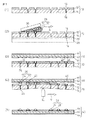
図1に、本発明の一実施形態によるはんだボールの搭載方法を示す。
FIG. 1 shows a solder ball mounting method according to an embodiment of the present invention.
先ず、図1(1)に示すように、はんだボール仮配置板10は、はんだボールの搭載位置にはんだボール受容口16を有する位置決め層12と、支持層14とが積層して成る。支持層14は位置決め層12のはんだボール受容口16の部位に、後出のフラックスが透過する貫通孔18を備えている。
First, as shown in FIG. 1A, the solder ball
配列するはんだボールの直径が100μmである場合、各部の寸法例は、下記のとおりである。 When the diameter of the solder balls to be arranged is 100 μm, the dimension example of each part is as follows.
はんだボール受容口16の開口径:140μm
位置決め層12の厚さ:100μm
支持層14の厚さ:50μm
はんだボール受容口16の開口ピッチ:200μm
位置決め層12は、Ni等のアディティブめっき等により作製することができる。支持層14は、Ni等のアディティブめっき等により作製することができるし、樹脂基板を加工して作製することもできる。
Solder
Solder
The
次に、図1(2)に示すように、ステージ20上に布、紙などのフラックス吸収シート22を載置し、その上にはんだボール仮配置板10を載置し、はんだボール仮配置板10の裏面をフラックス吸収シート22に密着させる。
Next, as shown in FIG. 1 (2), a
この状態で、はんだボール24をフラックス26中に分散させたペースト28を、はんだボール仮配置板10の位置決め層12側から刷り込んで、各はんだボール受容口16内に各1個のはんだボール24を含むペースト28を保持させる。ペースト28の刷り込みは図示のようにスキージ30を矢印Aの方向に操作することにより行なうこともできるし、後に説明するように位置決め層12上でのピストン加圧により行なうこともできる。
In this state, the
受容口16に注入されたペースト28のはんだボール24は受容口16内に保持され、フラックス26は受容口16内のはんだボール24が占める空間以外の部分を満たす。余剰のフラックス26は貫通孔18を通って、仮配置板10の裏面に密着配置されているフラックス吸収シート22に吸収される。これにより、仮配置板10の表面での余剰フラックスの残留と、ステージ20の汚れとを防止することができる。
The
ここで用いるフラックス26は、基本的には一般にスクリーン印刷に用いられるはんだペーストのはんだ粒子以外の部分と同様な成分でよいし、刷り込みに適した流動性を備えると同時に、受容口に保持された状態および接続パッドに転写された状態ではんだボール24を確実に付着固定するために適した粘着性を発揮できるように、成分配合を適宜調整することができる。
The
次に、図1(3)に示すように、はんだボール仮配置板10をステージ20および吸収シート22から取り外し、はんだボール受容口16を基板40の接続パッド46に位置合わせして保持する。なお、図では仮配置板10は前工程の刷り込み時と同じく上向きに示したが、これは上下反転させるためのスペースを不要とするためであり、反転のための十分なスペースを確保して不都合がなければ、下向き反転させた状態で以降の工程を行なっても何ら差し支えない。
Next, as shown in FIG. 1 (3), the solder ball
基板40は、スルーホール等を備えた樹脂製コア基板の両面にビルドアップ法などにより配線層と絶縁層を積層した多層回路基板であり、多層回路部42の表裏両面にソルダーレジスト層44が形成され、多層回路部42の表面(図の下面)に多数配列された接続パッド46がソルダーレジスト層44の開口48に露出している。
The
次に、図1(4)に示すように、各はんだボール受容口16内に保持されたペースト28を各接続パッド46に転写することにより、接続パッド46上にフラックス26を伴ったはんだボール24を搭載する。
Next, as shown in FIG. 1 (4), by transferring the
この転写は、図示したように、通常のスクリーン印刷における転写方法と同じく、仮配置板10の裏面の一部をスキージ等の押圧子50により押圧して基板40の表面に押し当てながら押圧子50を矢印Mのように水平に移動させることにより行なう。この転写方法では、仮配置板10が図のように撓むことにより局部的に押圧されるので、仮配置板10はそのために十分な可撓性を備えるように、材質や厚さを選定する。
As shown in the drawing, this transfer is performed by pressing a part of the rear surface of the
最後に、図1(5)に示すように、仮配置板10を取り外すと、基板40の接続パッド46上にはんだボール24がフラックス26で付着固定されて配列された状態が得られる。
Finally, as shown in FIG. 1 (5), when the
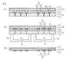
〔実施形態2〕
図2に、仮配置板10へのペースト28の刷り込みを、位置決め層12上でのピストン加圧により行なう実施形態を示す。仮配置板10は、実施形態1とは異なり支持層14Xがメッシュから成る。ただし、これは単に一つの選択肢を示したのであって、仮配置板10を特にこの場合にメッシュに限定する必要はなく、実施形態1と同様にメッシュ状ではなく貫通孔18を有する形態でもよい。
[Embodiment 2]
FIG. 2 shows an embodiment in which the
シリンダ52内でピストン54がピストン軸56の上下動により矢印P方向に上下に摺動するピストン加圧器58で、はんだボール24とフラックス26とから成るペースト28を位置決め層12上から刷り込んで、はんだボール24を1個含むペースト28をはんだボール受容口16内に注入する。
In the
受容口16に注入されたペースト28のはんだボール24は受容口16内に保持され、フラックス26は受容口16内のはんだボール24が占める空間以外の部分を満たす。余剰のフラックス26は支持層14Xのメッシュを通って、仮配置板10の裏面に密着配置されているフラックス吸収シート22に吸収される。これにより、仮配置板10の表面での余剰フラックスの残留と、ステージ20の汚れとを防止することができる。
The
ピストン加圧器58を矢印Aのように移動して、次のはんだボール配列予定区域で、上記と同様な操作を行ない、配列/移動を繰返すことにより、基板40全面あるいは必要部分に対応する仮配置板10上にはんだボールを配列することができる。
The
〔実施形態3〕
図3に、はんだボール仮配置板10のはんだボール受容口16から基板40の接続パッド46へのペースト28の転写を、支持層14の裏面側からのエアーブローによって行なう実施形態を示す。エアブローは、大気や窒素ガス等、何らかの気体の噴射による。実施形態1においては、このペースト28の上記転写を通常のスクリーン印刷における転写方法と同じく、スキージ等の押圧子50により仮配置板10を撓ませることにより行なうので、仮配置板10はそのために十分な可撓性を備えるように、材質や厚さに制限があった。本実施形態の方法によれば、仮配置板10は上記のような可撓性を必要としない。
[Embodiment 3]
FIG. 3 shows an embodiment in which the transfer of the
図3(1)に示すように、実施形態1または2などの方法により、はんだボール24を仮配置板10に仮配置する。仮配置板10と基板40とを位置合わせした後、両者を接近させて、下記のエアーブローによる転写に適した間隔(数十μm)に保持する。
As shown in FIG. 3A, the
次に図3(2)に示すように、仮配置板10の裏面にエアーブローユニット60を密着配置し、下方からエアーブローBを行ない、ペースト28を上方に吹き上げて、仮配置板10の直上数十μmにある基板40の各接続パッド46にはんだボール24各1個とフラックス26とから成るペースト28を注入する。
Next, as shown in FIG. 3 (2), an
図には、エアーブローユニット60を2個同時に作動させて、2つの配列予定区域に同時に配列を行なう例を示した。このように、複数の配列予定区域に対して同時に配列操作を行なうことにより、配列を高い効率で行なうことができる。ただし、特にこれに限定する必要はなく、エアーブローユニット60を1個用いて、配列予定区域を1つずつ処理することもできる。
In the figure, an example is shown in which two
最後に、図3(3)に示すように、仮配置板10を取り外すと、基板40の接続パッド46上にはんだボール24がフラックス26で付着固定されて配列された状態が得られる。
Finally, as shown in FIG. 3 (3), when the
〔実施形態4〕
図4に、仮配置板10をシリコンウェハの加工により一体として作製する例を示す。
[Embodiment 4]
FIG. 4 shows an example in which the
図4(1)に、作製する一体物のシリコンウェハ製仮配置板10を示す。仮配置板10は、位置決め層12Sと支持層14Sとが連続している一体構造である。位置決め層12Sにはんだボール受容口16Sがあり、支持層14Sに貫通孔18Sがある。
FIG. 4A shows an integrated silicon wafer
これを作製するために、先ず、図4(2)に示すように、シリコンウェハ70’を用意し、図2(3)に示すように研磨により所定の厚さ(例えば500μm)のシリコン素板70にする。
In order to produce this, first, as shown in FIG. 4 (2), a
図4(4)に示すように、シリコン素板70の表面に、スピンコート、露光、現像によりレジストパターン72を形成する。レジストパターン72は、はんだボール受容口16Sの口径と位置に対応する開口74を有する。
As shown in FIG. 4D, a resist
図4(5)に示すように、レジストパターン72をマスクとしてシリコン素板70のエッチングを行ない、シリコン素板70の表面にはんだボール受容口16Sとしての穴を掘り込む。このエッチングは、SF6等のガスを用いたドライエッチングや、TMAH(水酸化テトラエチルアンモニウム)、KOHなどを用いたウェットエッチングによって行なうことができる。はんだボール径が100μmの場合、受容口16Sの寸法は、例えば開口径140μm、深さ100μm、開口ピッチ200μmである。受容口16Sの深さは、位置決め層12Sの厚さでもある。
As shown in FIG. 4 (5), the
図4(6)に示すように、レジストパターン72を除去する。
As shown in FIG. 4 (6), the resist
図4(7)に示すように、シリコン素板70の裏面に、スピンコート、露光、現像によりレジストパターン78を形成する。レジストパターン78は、貫通孔18Sの口径と位置に対応する開口80を有する。
As shown in FIG. 4 (7), a resist
次いで、レジストパターン78をマスクとしてシリコン素板70のエッチングを行ない、シリコン素板70の裏面からはんだボール受容口16Sまで貫通する貫通孔18Sを掘り込む。このエッチングは、上記と同様に、SF6ガスを用いたドライエッチングや、TMAH(水酸化テトラエチルアンモニウム)、KOHなどを用いたウェットエッチングによって行なうことができる。はんだボール径が100μmの場合、貫通孔18Sの寸法は、例えば開口径80μm、長さ400μmである。貫通孔18Sの長さは、支持層14Sの厚さでもある。
Next, the
次いで、レジストパターン78を除去する。
Next, the resist
これにより、図4(8)に示したように、シリコン素板70の裏面から受容口16まで貫通する貫通孔18Sが形成される。
As a result, as shown in FIG. 4 (8), a through
以上の処理により、図4(1)に示したように、はんだボール受容口16Sを有する位置決め層12Sと貫通孔18Sを有する支持層14Sとから成るシリコン製のはんだボール仮配置板10が作製される。
As a result of the above processing, as shown in FIG. 4A, the silicon solder ball
以上説明したように、本発明はマスクを用いることなくはんだボールを接続パッドに配置することができるので、従来は不可避であったマスクへのフラックス付着が起きることがない。 As described above, according to the present invention, since solder balls can be arranged on connection pads without using a mask, flux adhesion to the mask, which has been unavoidable in the past, does not occur.
また、はんだボールとフラックスとから成るペーストを接続パッドに配置するので、接続パッドへフラックスを塗布する別途の工程が不要であり、ボールとフラックスとを同時に配置できる。 Further, since the paste composed of the solder balls and the flux is disposed on the connection pads, a separate process for applying the flux to the connection pads is not required, and the balls and the flux can be disposed simultaneously.
本発明によれば、マスクへのフラックス付着によるはんだボールの搭載不良を起こすことなく、微小はんだボールを基板の接続パッドに配置することができるはんだボールの配列方法が提供される。 ADVANTAGE OF THE INVENTION According to this invention, the arrangement | positioning method of the solder ball which can arrange | position a micro solder ball to the connection pad of a board | substrate is caused without causing the mounting defect of the solder ball by the flux adhesion to a mask.
10 はんだボール仮配置板
12、12S 位置決め層
14、14X、14S 支持層
16、16S はんだボール受容口
18、18S 貫通孔
20 ステージ
22 フラックス吸収シート
24 はんだボール
26 フラックス
28 ペースト
30 スキージ
40 基板
42 多層回路部
44 ソルダーレジスト層
46 接続パッド
48 開口
50 押圧子
52 シリンダ
54 ピストン
56 ピストン軸
60 エアーブローユニット
70 シリコン素板
70’ シリコンウェハ
72 レジストパターン
74 開口
78 レジストパターン
80 開口
DESCRIPTION OF
Claims (8)
導電性ボールの搭載位置に導電性ボール受容口を有する位置決め層と支持層とが積層して成る導電性ボール仮配置板であって、該支持層は少なくとも該位置決め層の導電性ボール受容口の部位では下記フラックスを透過可能である導電性ボール仮配置板を用い、
導電性ボールをフラックス中に分散させたペーストを、上記導電性ボール仮配置板の位置決め層側から刷り込んで、各導電性ボール受容口内に各1個の導電性ボールを含むペーストを保持させ、
上記導電性ボール仮配置板の導電性ボール受容口を上記基板の接続パッドに位置合わせして、各導電性ボール受容口内に保持されたペーストを各接続パッドに転写することにより、接続パッド上にフラックスを伴った導電性ボールを搭載することを特徴とする導電性ボールの搭載方法。 A method of mounting one conductive ball on each of a plurality of connection pads on a substrate,
A conductive ball temporary arrangement plate in which a positioning layer having a conductive ball receiving port at a mounting position of a conductive ball and a support layer are laminated, and the support layer is at least a conductive ball receiving port of the positioning layer. In the part, using a conductive ball temporary arrangement plate that can penetrate the following flux,
A paste in which conductive balls are dispersed in a flux is imprinted from the positioning layer side of the conductive ball temporary placement plate to hold a paste containing one conductive ball in each conductive ball receiving port,
The conductive ball receiving port of the conductive ball temporary arrangement plate is aligned with the connection pad of the substrate, and the paste held in each conductive ball receiving port is transferred to each connection pad. A conductive ball mounting method comprising mounting a conductive ball with a flux.
Priority Applications (2)
| Application Number | Priority Date | Filing Date | Title |
|---|---|---|---|
| JP2007188630A JP4895936B2 (en) | 2007-07-19 | 2007-07-19 | Mounting method of conductive balls |
| US12/173,256 US7820479B2 (en) | 2007-07-19 | 2008-07-15 | Conductive ball mounting method |
Applications Claiming Priority (1)
| Application Number | Priority Date | Filing Date | Title |
|---|---|---|---|
| JP2007188630A JP4895936B2 (en) | 2007-07-19 | 2007-07-19 | Mounting method of conductive balls |
Publications (3)
| Publication Number | Publication Date |
|---|---|
| JP2009026959A JP2009026959A (en) | 2009-02-05 |
| JP2009026959A5 JP2009026959A5 (en) | 2010-06-17 |
| JP4895936B2 true JP4895936B2 (en) | 2012-03-14 |
Family
ID=40264027
Family Applications (1)
| Application Number | Title | Priority Date | Filing Date |
|---|---|---|---|
| JP2007188630A Expired - Fee Related JP4895936B2 (en) | 2007-07-19 | 2007-07-19 | Mounting method of conductive balls |
Country Status (2)
| Country | Link |
|---|---|
| US (1) | US7820479B2 (en) |
| JP (1) | JP4895936B2 (en) |
Cited By (1)
| Publication number | Priority date | Publication date | Assignee | Title |
|---|---|---|---|---|
| KR20180035676A (en) * | 2016-09-29 | 2018-04-06 | 신꼬오덴기 고교 가부시키가이샤 | Carrier base material-added wiring substrate and method for manufacturing carrier base material-added wiring substrate |
Families Citing this family (23)
| Publication number | Priority date | Publication date | Assignee | Title |
|---|---|---|---|---|
| US20110017581A1 (en) * | 2009-07-23 | 2011-01-27 | Keith Bryan Hardin | Z-Directed Switch Components for Printed Circuit Boards |
| US8198547B2 (en) | 2009-07-23 | 2012-06-12 | Lexmark International, Inc. | Z-directed pass-through components for printed circuit boards |
| US8198548B2 (en) * | 2009-07-23 | 2012-06-12 | Lexmark International, Inc. | Z-directed capacitor components for printed circuit boards |
| US8735734B2 (en) | 2009-07-23 | 2014-05-27 | Lexmark International, Inc. | Z-directed delay line components for printed circuit boards |
| US8237061B2 (en) * | 2009-07-23 | 2012-08-07 | Lexmark International, Inc. | Z-directed filter components for printed circuit boards |
| US8273996B2 (en) * | 2009-07-23 | 2012-09-25 | Lexmark International, Inc. | Z-directed connector components for printed circuit boards |
| US8278568B2 (en) * | 2009-07-23 | 2012-10-02 | Lexmark International, Inc. | Z-directed variable value components for printed circuit boards |
| US20110017504A1 (en) * | 2009-07-23 | 2011-01-27 | Keith Bryan Hardin | Z-Directed Ferrite Bead Components for Printed Circuit Boards |
| US20110017502A1 (en) * | 2009-07-23 | 2011-01-27 | Keith Bryan Hardin | Z-Directed Components for Printed Circuit Boards |
| WO2012099602A1 (en) * | 2011-01-21 | 2012-07-26 | Lexmark International, Inc. | Z-directed connector components for printed circuit boards |
| US9078374B2 (en) | 2011-08-31 | 2015-07-07 | Lexmark International, Inc. | Screening process for manufacturing a Z-directed component for a printed circuit board |
| US8658245B2 (en) | 2011-08-31 | 2014-02-25 | Lexmark International, Inc. | Spin coat process for manufacturing a Z-directed component for a printed circuit board |
| US8790520B2 (en) | 2011-08-31 | 2014-07-29 | Lexmark International, Inc. | Die press process for manufacturing a Z-directed component for a printed circuit board |
| US9009954B2 (en) | 2011-08-31 | 2015-04-21 | Lexmark International, Inc. | Process for manufacturing a Z-directed component for a printed circuit board using a sacrificial constraining material |
| US8752280B2 (en) | 2011-09-30 | 2014-06-17 | Lexmark International, Inc. | Extrusion process for manufacturing a Z-directed component for a printed circuit board |
| US8943684B2 (en) * | 2011-08-31 | 2015-02-03 | Lexmark International, Inc. | Continuous extrusion process for manufacturing a Z-directed component for a printed circuit board |
| US8830692B2 (en) | 2012-03-29 | 2014-09-09 | Lexmark International, Inc. | Ball grid array systems for surface mounting an integrated circuit using a Z-directed printed circuit board component |
| US8822838B2 (en) | 2012-03-29 | 2014-09-02 | Lexmark International, Inc. | Z-directed printed circuit board components having conductive channels for reducing radiated emissions |
| US8822840B2 (en) | 2012-03-29 | 2014-09-02 | Lexmark International, Inc. | Z-directed printed circuit board components having conductive channels for controlling transmission line impedance |
| US8912452B2 (en) | 2012-03-29 | 2014-12-16 | Lexmark International, Inc. | Z-directed printed circuit board components having different dielectric regions |
| KR102029077B1 (en) | 2013-02-04 | 2019-10-07 | 삼성전자주식회사 | Method of forming external terminals of a package and apparatus for performing the same |
| US9673131B2 (en) * | 2013-04-09 | 2017-06-06 | Intel Corporation | Integrated circuit package assemblies including a glass solder mask layer |
| US9216469B2 (en) * | 2013-10-18 | 2015-12-22 | Taiwan Semiconductor Manufacturing Co., Ltd. | Indirect printing bumping method for solder ball deposition |
Family Cites Families (9)
| Publication number | Priority date | Publication date | Assignee | Title |
|---|---|---|---|---|
| US5284287A (en) * | 1992-08-31 | 1994-02-08 | Motorola, Inc. | Method for attaching conductive balls to a substrate |
| US5431332A (en) * | 1994-02-07 | 1995-07-11 | Motorola, Inc. | Method and apparatus for solder sphere placement using an air knife |
| US5655704A (en) * | 1994-08-30 | 1997-08-12 | Matsushita Electric Industrial Co., Ltd. | Method and apparatus for mounting soldering balls onto electrodes of a substrate or a comparable electronic component |
| CA2135508C (en) * | 1994-11-09 | 1998-11-03 | Robert J. Lyn | Method for forming solder balls on a semiconductor substrate |
| JPH09107045A (en) | 1995-10-13 | 1997-04-22 | Japan Aviation Electron Ind Ltd | Ball mounting method for bga package |
| JPH10126046A (en) | 1996-10-18 | 1998-05-15 | Oki Electric Ind Co Ltd | Equipment for manufacturing ball grid array |
| JP2925534B1 (en) * | 1998-04-28 | 1999-07-28 | 株式会社日鉄マイクロメタル | Metal ball arrangement method and arrangement device |
| US6191022B1 (en) * | 1999-04-18 | 2001-02-20 | Cts Corporation | Fine pitch solder sphere placement |
| JP2001320160A (en) | 2000-05-12 | 2001-11-16 | Fuji Photo Film Co Ltd | Cream solder application method, and solder supplying device |
-
2007
- 2007-07-19 JP JP2007188630A patent/JP4895936B2/en not_active Expired - Fee Related
-
2008
- 2008-07-15 US US12/173,256 patent/US7820479B2/en not_active Expired - Fee Related
Cited By (2)
| Publication number | Priority date | Publication date | Assignee | Title |
|---|---|---|---|---|
| KR20180035676A (en) * | 2016-09-29 | 2018-04-06 | 신꼬오덴기 고교 가부시키가이샤 | Carrier base material-added wiring substrate and method for manufacturing carrier base material-added wiring substrate |
| KR102394215B1 (en) * | 2016-09-29 | 2022-05-09 | 신꼬오덴기 고교 가부시키가이샤 | Carrier base material-added wiring substrate and method for manufacturing carrier base material-added wiring substrate |
Also Published As
| Publication number | Publication date |
|---|---|
| US20090020591A1 (en) | 2009-01-22 |
| US7820479B2 (en) | 2010-10-26 |
| JP2009026959A (en) | 2009-02-05 |
Similar Documents
| Publication | Publication Date | Title |
|---|---|---|
| JP4895936B2 (en) | Mounting method of conductive balls | |
| JP4393538B2 (en) | Magnetic solder ball arrangement apparatus and arrangement method | |
| TWI345436B (en) | ||
| US6316289B1 (en) | Method of forming fine-pitch interconnections employing a standoff mask | |
| JP4503053B2 (en) | Conductive ball mounting apparatus and mounting method | |
| WO2009144846A1 (en) | Solder ball mounting method | |
| KR20120108952A (en) | Method of manufacturing circuit board, and method of manufacturing electronic device | |
| US20220078921A1 (en) | Method of producing circuit boards | |
| US6303881B1 (en) | Via connector and method of making same | |
| US6722275B2 (en) | Reservoir stencil with relief areas and method of using | |
| US6569248B1 (en) | Apparatus for selectively applying solder mask | |
| JP4118286B2 (en) | Solder ball mounting method | |
| JP2006261187A (en) | Method of manufacturing substrate with built-in component | |
| JP2003264255A (en) | Method of manufacturing wiring board | |
| KR100754086B1 (en) | Probe Card and Method of Fabrication thereof | |
| KR100855822B1 (en) | Apparatus and Method of Printing the Pattern on the Substrate | |
| JP2000307221A (en) | Electric connection method for electronic part | |
| JP2007253593A (en) | Screen printing method | |
| JP2018202774A (en) | Paste-embedding printer | |
| KR20040110565A (en) | Metal mask and method of manufacture thereof, and method of manufacturing multi-layered printed circuit board using thereof | |
| JP5067107B2 (en) | Circuit board and semiconductor device | |
| KR100842255B1 (en) | Mask and method for manufacturing thereof | |
| JP2006319255A (en) | Process for manufacturing multilayer wiring board | |
| JP2015012056A (en) | Solder ball mounting method | |
| JPH10321678A (en) | Conductive particle arrangement method and conductive particle arrangement tape |
Legal Events
| Date | Code | Title | Description |
|---|---|---|---|
| A521 | Request for written amendment filed |
Free format text: JAPANESE INTERMEDIATE CODE: A523 Effective date: 20100428 |
|
| A621 | Written request for application examination |
Free format text: JAPANESE INTERMEDIATE CODE: A621 Effective date: 20100428 |
|
| A977 | Report on retrieval |
Free format text: JAPANESE INTERMEDIATE CODE: A971007 Effective date: 20111115 |
|
| TRDD | Decision of grant or rejection written | ||
| A01 | Written decision to grant a patent or to grant a registration (utility model) |
Free format text: JAPANESE INTERMEDIATE CODE: A01 Effective date: 20111122 |
|
| A01 | Written decision to grant a patent or to grant a registration (utility model) |
Free format text: JAPANESE INTERMEDIATE CODE: A01 |
|
| A61 | First payment of annual fees (during grant procedure) |
Free format text: JAPANESE INTERMEDIATE CODE: A61 Effective date: 20111220 |
|
| R150 | Certificate of patent or registration of utility model |
Free format text: JAPANESE INTERMEDIATE CODE: R150 |
|
| FPAY | Renewal fee payment (event date is renewal date of database) |
Free format text: PAYMENT UNTIL: 20150106 Year of fee payment: 3 |
|
| LAPS | Cancellation because of no payment of annual fees |