WO2009144846A1 - 半田ボール搭載方法 - Google Patents
半田ボール搭載方法 Download PDFInfo
- Publication number
- WO2009144846A1 WO2009144846A1 PCT/JP2008/067170 JP2008067170W WO2009144846A1 WO 2009144846 A1 WO2009144846 A1 WO 2009144846A1 JP 2008067170 W JP2008067170 W JP 2008067170W WO 2009144846 A1 WO2009144846 A1 WO 2009144846A1
- Authority
- WO
- WIPO (PCT)
- Prior art keywords
- mask
- solder ball
- solder
- printed wiring
- wiring board
- Prior art date
Links
Images


Classifications
-
- H—ELECTRICITY
- H05—ELECTRIC TECHNIQUES NOT OTHERWISE PROVIDED FOR
- H05K—PRINTED CIRCUITS; CASINGS OR CONSTRUCTIONAL DETAILS OF ELECTRIC APPARATUS; MANUFACTURE OF ASSEMBLAGES OF ELECTRICAL COMPONENTS
- H05K3/00—Apparatus or processes for manufacturing printed circuits
- H05K3/30—Assembling printed circuits with electric components, e.g. with resistor
- H05K3/32—Assembling printed circuits with electric components, e.g. with resistor electrically connecting electric components or wires to printed circuits
- H05K3/34—Assembling printed circuits with electric components, e.g. with resistor electrically connecting electric components or wires to printed circuits by soldering
- H05K3/3457—Solder materials or compositions; Methods of application thereof
- H05K3/3478—Applying solder preforms; Transferring prefabricated solder patterns
-
- B—PERFORMING OPERATIONS; TRANSPORTING
- B23—MACHINE TOOLS; METAL-WORKING NOT OTHERWISE PROVIDED FOR
- B23K—SOLDERING OR UNSOLDERING; WELDING; CLADDING OR PLATING BY SOLDERING OR WELDING; CUTTING BY APPLYING HEAT LOCALLY, e.g. FLAME CUTTING; WORKING BY LASER BEAM
- B23K3/00—Tools, devices, or special appurtenances for soldering, e.g. brazing, or unsoldering, not specially adapted for particular methods
- B23K3/06—Solder feeding devices; Solder melting pans
- B23K3/0607—Solder feeding devices
- B23K3/0623—Solder feeding devices for shaped solder piece feeding, e.g. preforms, bumps, balls, pellets, droplets
-
- B—PERFORMING OPERATIONS; TRANSPORTING
- B23—MACHINE TOOLS; METAL-WORKING NOT OTHERWISE PROVIDED FOR
- B23K—SOLDERING OR UNSOLDERING; WELDING; CLADDING OR PLATING BY SOLDERING OR WELDING; CUTTING BY APPLYING HEAT LOCALLY, e.g. FLAME CUTTING; WORKING BY LASER BEAM
- B23K3/00—Tools, devices, or special appurtenances for soldering, e.g. brazing, or unsoldering, not specially adapted for particular methods
- B23K3/06—Solder feeding devices; Solder melting pans
- B23K3/0646—Solder baths
- B23K3/0692—Solder baths with intermediary means for bringing solder on workpiece, e.g. rollers
-
- B—PERFORMING OPERATIONS; TRANSPORTING
- B23—MACHINE TOOLS; METAL-WORKING NOT OTHERWISE PROVIDED FOR
- B23K—SOLDERING OR UNSOLDERING; WELDING; CLADDING OR PLATING BY SOLDERING OR WELDING; CUTTING BY APPLYING HEAT LOCALLY, e.g. FLAME CUTTING; WORKING BY LASER BEAM
- B23K2101/00—Articles made by soldering, welding or cutting
- B23K2101/36—Electric or electronic devices
-
- H—ELECTRICITY
- H05—ELECTRIC TECHNIQUES NOT OTHERWISE PROVIDED FOR
- H05K—PRINTED CIRCUITS; CASINGS OR CONSTRUCTIONAL DETAILS OF ELECTRIC APPARATUS; MANUFACTURE OF ASSEMBLAGES OF ELECTRICAL COMPONENTS
- H05K2203/00—Indexing scheme relating to apparatus or processes for manufacturing printed circuits covered by H05K3/00
- H05K2203/04—Soldering or other types of metallurgic bonding
- H05K2203/041—Solder preforms in the shape of solder balls
-
- H—ELECTRICITY
- H05—ELECTRIC TECHNIQUES NOT OTHERWISE PROVIDED FOR
- H05K—PRINTED CIRCUITS; CASINGS OR CONSTRUCTIONAL DETAILS OF ELECTRIC APPARATUS; MANUFACTURE OF ASSEMBLAGES OF ELECTRICAL COMPONENTS
- H05K2203/00—Indexing scheme relating to apparatus or processes for manufacturing printed circuits covered by H05K3/00
- H05K2203/04—Soldering or other types of metallurgic bonding
- H05K2203/0485—Tacky flux, e.g. for adhering components during mounting
-
- H—ELECTRICITY
- H05—ELECTRIC TECHNIQUES NOT OTHERWISE PROVIDED FOR
- H05K—PRINTED CIRCUITS; CASINGS OR CONSTRUCTIONAL DETAILS OF ELECTRIC APPARATUS; MANUFACTURE OF ASSEMBLAGES OF ELECTRICAL COMPONENTS
- H05K2203/00—Indexing scheme relating to apparatus or processes for manufacturing printed circuits covered by H05K3/00
- H05K2203/05—Patterning and lithography; Masks; Details of resist
- H05K2203/0548—Masks
- H05K2203/0557—Non-printed masks
-
- H—ELECTRICITY
- H05—ELECTRIC TECHNIQUES NOT OTHERWISE PROVIDED FOR
- H05K—PRINTED CIRCUITS; CASINGS OR CONSTRUCTIONAL DETAILS OF ELECTRIC APPARATUS; MANUFACTURE OF ASSEMBLAGES OF ELECTRICAL COMPONENTS
- H05K3/00—Apparatus or processes for manufacturing printed circuits
- H05K3/30—Assembling printed circuits with electric components, e.g. with resistor
- H05K3/32—Assembling printed circuits with electric components, e.g. with resistor electrically connecting electric components or wires to printed circuits
- H05K3/34—Assembling printed circuits with electric components, e.g. with resistor electrically connecting electric components or wires to printed circuits by soldering
- H05K3/3489—Composition of fluxes; Methods of application thereof; Other methods of activating the contact surfaces
Definitions
- the present invention relates to a solder ball mounting method for mounting solder balls to be solder bumps on a printed wiring board.
- solder bumps are used for electrical connection between the printed wiring board and the IC chip.
- the solder bump is formed by the following process. (1) A step of printing flux on connection pads formed on the printed wiring board. (2) A step of mounting solder balls on connection pads on which flux is printed. (3) A step of reflowing to form solder bumps from the solder balls.
- a mask having an opening for dropping the solder ball onto the mounted body is used.
- spacers are formed from a plurality of protrusions.
- a mask is aligned with respect to a to-be-mounted body so that a projection part may be arrange
- the flux adheres to the tip of the protrusion, making it difficult to remove the mask from the substrate.
- the substrate may be warped by stress when removing the mask.
- the solder ball is displaced from the electrode portion due to the reaction at that time.
- An object of the present invention is to provide a solder ball mounting method capable of reliably mounting a solder ball on a connection pad.
- the invention of claim 1 is a solder ball mounting method for mounting a solder ball to be a solder bump on a connection pad of a printed wiring board: Applying a flux to the surface of the connection pad of the printed wiring board; Preparing a mask comprising a mask body having an opening group consisting of a plurality of openings corresponding to the connection pads, and a spacer having an opening for exposing the opening group; Positioning the mask with respect to the printed wiring board such that the opening of the mask body faces the connection pad; And a step of supplying a solder ball onto the mask and dropping the solder ball onto the connection pad through an opening of the mask main body.
- the flux can be collectively applied to the connection pad forming region of the printed wiring board, and manufactured compared to the case where the flux is locally applied to each connection pad.
- the process can be simplified. Further, since no connection pads to which flux is not applied are generated, solder balls can be reliably mounted on each connection pad.
- the spacer integrally with the mask main body, the height of the mask can be strictly controlled, and the height of the solder ball and the mask upper surface can be easily matched.
- one solder ball can be reliably mounted on the connection pad, and the probability of occurrence of a defect due to the solder ball not being mounted or mounting a plurality of solder balls can be reduced.
- FIG. 3 shows a sheet-sized printed wiring board 10 on which solder balls are mounted using the mask according to the first embodiment.
- the sheet-sized printed wiring board 10 is for taking a large number of pieces to manufacture a printed wiring board 10R having a piece size of 4 ⁇ 4, for example. 16 pieces of printed wiring boards 10R are manufactured along the chain line Z in the figure.
- a connection pad forming region 75g formed with a plurality of connection pads 75 on which solder balls are mounted.
- the connection pad formation region means a specific region having a minimum area among regions including all the connection pads of the printed wiring board.
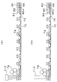
- FIG. 1 is a back view of a mask 80 according to the first embodiment for mounting solder balls on the printed wiring board shown in FIG.
- the mask 80 includes a mask main body 82 in which an opening group 84g including openings 84 corresponding to the connection pads 75 of the printed wiring board 10 is formed, and a spacer 86 in which an opening 86a that exposes the opening group 84g is formed.
- the mask body 82 and the spacer 86 are integrally formed.
- the term “integrally” as used herein includes not only those formed by the same process, but also those in which the same substance or different ones are separately fixed.
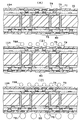
- FIG. 2 shows the mask main body 82 and the spacer 86 separately
- FIG. 2A is a plan view of the mask main body 82
- FIG. 2B is a plan view of the spacer 86.
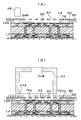
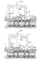
- FIG. 4A corresponds to the AA cross section in FIG. 1, and shows a state where the mask 80 is placed on the printed wiring board 10, and FIG. 4B shows a circle in FIG. 4A.
- part shown by b is expanded and shown.
- a solder resist layer 70 is formed on the surface of the printed wiring board 10, and the connection pads 75 are exposed from the openings 71 formed in the solder resist layer 70.
- a flux 79 is applied to the entire connection pad formation region 75g of the printed wiring board 10. The application area of the flux is smaller than the opening of the spacer. That is, the flux 79 is applied to the connection pad forming region 75g so as to avoid the contact portion with the spacer 86 in the printed wiring board 10.
- the flux 79 is applied to the connection pad forming region 75g while avoiding the contact portion between the spacer 86 and the printed wiring board 10. For this reason, since the flux does not adhere to the spacer 86, problems such as warpage of the printed wiring board, displacement of the solder ball with respect to the connection pad, and damage to the solder resist layer 70 when the mask is removed from the printed wiring board do not occur. .
- the thickness of the mask 80 is set so that the height of the top surface of the mask 80 and the top of the solder ball 78 are substantially aligned with the solder ball 78 mounted on the connection pad 75. Even.
- the thickness h1 of the mask body 82 is set to 25 ⁇ m
- the thickness h2 of the spacer 86 is set to 30 ⁇ m
- the thickness h3 of the solder resist layer from the upper surface of the connection pad 75 is set to 15 ⁇ m.
- the “top portion of the solder ball” means a portion having the highest height on the surface of the solder ball.
- solder ball mounting method of the first embodiment a predetermined amount (one by one) of solder balls can be reliably mounted on the electrode pad 75 by matching the heights of the solder balls 78 and the upper surface of the mask 80. In addition, it is possible to reduce the probability of occurrence of defects due to the solder balls not being mounted or mounting a plurality of solder balls.
- FIG. 19 when the height of the upper surface of the mask 80 is higher than the height of the solder ball 78, another solder ball is mounted on the solder ball mounted on the connection pad through the opening of the mask body. Will be.
- solder balls protrude from the upper surface of the mask 80 in this way, it becomes an obstacle when mounting the solder balls on other connection pads, which is not preferable. Furthermore, when reflowing is performed in this state, the solder bumps have a large volume outside a predetermined range, resulting in a decrease in yield.
- the opening diameter of the mask body opening is preferably 1.2 to 1.5 times the diameter of the solder ball. That is, for example, when using a solder ball having a diameter of 70 ⁇ m, the opening diameter is preferably 84 to 105 ⁇ m. Thereby, it is possible to securely mount the solder balls one by one on the connection pad. Here, if it is less than 1.2 times, it is not mounted on the connection pad. On the other hand, if it exceeds 1.5 times, the probability of mounting a plurality of solder balls on the connection pad increases.
- FIG. 7A is an explanatory diagram of mounting of solder balls by the mask 80 of the first embodiment.
- a cylindrical member 24 having an opening 24A facing the mask is positioned above the mask 80, and air is sucked by the cylindrical member 24 so that the solder balls 78 are gathered on the mask immediately below the cylindrical member 24. Then, by moving the cylindrical member 24 in the horizontal direction relative to the mask 80, the solder balls 78 assembled on the mask 80 are moved, and the solder balls 78 are dropped onto the connection pads 75.
- FIG. 7B shows a modification of the first embodiment. In FIG. 7A, air was sucked by the cylindrical member 24. On the other hand, in the modified example, air is blown out from the cylindrical member 24, the solder ball 78 is sent, and the solder ball 78 is dropped to the connection pad 75.
- the cylindrical member 24 is positioned above the mask 80, and air is sucked from the opening of the cylindrical member 24 to collect the solder balls 78.
- the assembled solder balls 78 are moved on the mask 80, and the solder balls 78 are dropped onto the connection pads 75 of the printed wiring board 10 through the openings 84 of the mask.
- fine solder balls can be reliably mounted on all connection pads of the printed wiring board.
- the solder ball is moved in a non-contact manner, unlike the case of using a squeegee, it can be mounted on the connection pad without damaging the solder ball, and the height of the solder bump can be made uniform.
- a solder ball can be appropriately placed on a connection pad even on a printed wiring board having a large undulation on the surface, such as a build-up multilayer wiring board.
- the portion where the opening group 84g of the mask main body 82 provided corresponding to the opening 86a of the spacer 86 is supported from four directions by the spacer 86 is difficult to bend.
- the distance from the wiring board 10 can be made constant. In particular, even if air is sucked by the cylindrical member 24, the flow of air passing through the gap between the mask 80 and the printed wiring board 10 is blocked by the spacer 86, and the mask body is lifted by the airflow passing through the opening group from below the mask. In addition, the distance between the mask body and the printed wiring board can always be kept constant.
- a plating resist 202 for forming a mask opening 84 is formed on the SUS plate 200 subjected to the surface treatment (FIG. 5A).
- a mask main body 82 having an opening 84 is formed by nickel alloy electroplating (FIG. 5B).
- a plating resist 204 serving as a spacer opening is formed on the mask body 82 (FIG. 5C).
- a spacer 86 having an opening 86a is formed by nickel alloy electroplating (FIG. 5D).
- the mask 80 including the spacer 86 and the mask body 82 is peeled from the SUS plate 200 (FIG. 5E).
- the thickness can be accurately adjusted by integrally forming the spacer 86 and the mask main body 82 by plating.
- the spacer 86 and the mask main body 82 are integrally formed.
- the spacer and the mask main body formed separately may be attached by, for example, ultrasonic bonding or an adhesive.
- the spacer and the mask body may be formed of different materials.
- the mask body can be made of metal and the spacer can be made of resin.
- the support is made of a material in which a nylon cloth 220 with a uniform tension applied to the frame 210 is affixed.
- a mask 80 is attached to the center of the nylon cloth 220 with an adhesive 222.
- the adhesive 222 is applied to the outer edge of the mask body 82 and outside the spacer 86.
- the uniform tension of the nylon cloth 220 is applied to the mask 80 by forming an opening 220 ⁇ / b> A in the nylon cloth 220 inside the adhesive 222.
- the outer edge of the mask body 82 extends beyond the outer edge of the spacer 86.
- uniform tension is applied to the portion where the spacer exists and the portion located in the opening of the spacer in the mask body. become. That is, a uniform tension is applied over the entire mask body.
- bending due to the tension difference is suppressed, the height of the mask body can be strictly controlled, and the height of the solder ball and the mask upper surface can be easily matched.
- a mask according to the second embodiment will be described with reference to FIG. 8 showing the back surface of the mask.
- the opening 86a of the spacer 86 is formed for each opening group 84g of the mask body.
- an opening 86a is formed in the spacer 86 so as to expose the plurality of opening groups 84g of the mask main body in a lump.
- solder ball mounting method A solder ball mounting method according to the third embodiment will be described with reference to FIG.
- the solder balls are transferred by airflow.
- solder balls are mounted on the connection pads by the brush 110.
- solder ball mounting method according to a modified example of the third embodiment will be described with reference to FIG.
- solder balls are mounted on the connection pads by a squeegee 112 having flexibility.
- solder ball mounting method A solder ball mounting method according to the fourth embodiment will be described with reference to FIG.
- the solder balls are transferred by airflow.
- solder balls are mounted on the connection pads by applying vibration to the mask 80 and the printed wiring board.
- solder ball mounting method according to a modified example of the fourth embodiment will be described with reference to FIG.
- the solder balls are conveyed by tilting the mask 80 and the printed wiring board.
- FIGS. 16 shows a cross-sectional view of the multilayer printed wiring board 10
- FIG. 17 shows a state in which the IC chip 90 is attached to the multilayer printed wiring board 10 shown in FIG.
- conductor circuits 34 are formed on both surfaces of the core substrate 30. The front surface and the back surface of the core substrate 30 are connected through a through hole 36.
- a conductor circuit 58 for forming a conductor circuit layer is formed on the conductor circuit 34 of the core substrate 30 via an interlayer resin insulating layer 50.
- the conductor circuit 58 is connected to the conductor circuit 34 via the via hole 60.
- a conductor circuit 158 is formed on the conductor circuit 58 via an interlayer resin insulation layer 150.
- Conductor circuit 158 is connected to conductor circuit 58 via via hole 160 formed in interlayer resin insulation layer 150.
- a solder resist layer 70 is formed above the via hole 160 and the conductor circuit 158.
- the connection pad 75 is formed.
- Solder bumps 78U are formed on the upper connection pads 75
- solder bumps 78D are formed on the lower connection pads 75.
- solder bumps 78 ⁇ / b> U on the upper surface side of the multilayer printed wiring board 10 are connected to the electrodes 92 of the IC chip 90.
- the lower solder bump 78D is connected to the land 96 of the daughter board 94.
- FIG. 18 is a plan view of a multi-layer printed wiring board 10A for taking multiple pieces (sheet size).
- the multilayer printed wiring board 10A is separated by cutting individual (piece size) multilayer printed wiring boards 10 each having a connection pad forming region 75g in which the connection pads 75 are arranged in a matrix shape, by cutting along a dashed line in the drawing.
- FIG. 15 is an explanatory diagram of a process of forming solder bumps on the multi-layer printed wiring board 10A for multi-piece taking, and corresponds to a cross-sectional view along Y1-Y1 in FIG.
- the flux 79 is collectively printed on the surface including the opening 71 of the solder resist layer 70 and the surface of the connection pad 75.
- FIG. 15A the flux 79 is collectively printed on the surface including the opening 71 of the solder resist layer 70 and the surface of the connection pad 75.
- a small solder ball 78s (for example, manufactured by Hitachi Metals, Ltd., having a diameter of 40 ⁇ m ⁇ or more, is formed on the connection pad 75 on the upper side of the multilayer printed wiring board 10A using a solder ball mounting device described later. (Less than 200 ⁇ m ⁇ ). In this case, if the diameter is less than 40 ⁇ m ⁇ , the solder ball is too light and it is difficult to drop it onto the connection pad. On the other hand, if the diameter exceeds 200 ⁇ m, it is too heavy, so that the solder balls cannot be assembled in the cylindrical member, and there are connection pads on which the solder balls are not placed.
- solder balls having a diameter of 40 ⁇ m ⁇ or more and less than 200 ⁇ m ⁇ it is highly significant to use solder balls having a diameter of 40 ⁇ m ⁇ or more and less than 200 ⁇ m ⁇ . In this range, it is advantageous for refinement as the diameter of the opening 71 of the solder resist layer 70 becomes smaller. Further, in the method in which the solder ball is sucked by the suction head and the solder ball is mounted on the connection pad, since the solder ball is small and difficult to be sucked, the superiority of the method of the embodiment becomes clear.
- solder ball 78L having a normal diameter is formed on the connection pad 75 on the lower side of the multilayer printed wiring board 10A with a suction head according to a conventional technique (for example, Japanese Patent No. 1975429). Is adsorbed and placed. Thereafter, it is heated in a reflow furnace, and as shown in FIG. 16, solder bumps 78U are formed on the upper side of the multilayer printed wiring board 10A at a pitch of 60 ⁇ m or more and less than 200 ⁇ m, for example, 500 to 30,000 solder bumps 78D at a pitch of 2 mm, For example, 250 pieces are formed.
- the pitch is less than 60 ⁇ m, it becomes difficult to manufacture solder balls suitable for the pitch.
- the pitch is 200 ⁇ m or more, the present method can be produced without any problem, but it can also be produced by a conventional method.
- the IC chip 90 is mounted via the solder bumps 78U by reflow.
- the multilayer printed wiring board 10 on which the IC chip 90 is mounted is attached to the daughter board 94 via the solder bumps 78D.
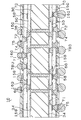
- FIG. 11A is a configuration diagram showing the configuration of the solder ball mounting apparatus according to the solder ball mounting method of the first embodiment, and FIG. 11B shows the solder ball mounting apparatus of FIG. It is an arrow view seen from the B side.
- the solder ball mounting device 20 includes an XY ⁇ suction table 14 that positions and holds the multilayer printed wiring board 10A, a vertical movement shaft 12 that raises and lowers the XY ⁇ suction table 14, and an opening that corresponds to the connection pad 75 of the multilayer printed wiring board.
- a ball alignment mask 80, a mounting cylinder (cylinder member) 24 for guiding a solder ball moving on the ball alignment mask 80, a suction box 26 for applying a negative pressure to the mounting cylinder 24, and excess solder balls are collected.
- a suction ball removing cylinder 61, a suction box 66 for applying a negative pressure to the suction ball removing cylinder 61, a suction ball removing suction device 68 for holding the collected solder balls, and a mask clamp for clamping the ball alignment mask 80 44, an X direction moving shaft 40 for sending the mounting cylinder 24 and the suction ball removing cylinder 61 in the X direction, and an X direction moving shaft 40 are supported.
- a solder ball supply device 22 for supplying a solder ball to the mounting cylinder 24 based on the detected remaining amount.
- the solder ball mounting apparatus 20 shown in FIG. 11 only the X-direction moving shaft 40 that sends the mounting cylinder 24 and the suction ball removing cylinder 61 in the X direction is shown, but a moving mechanism that sends in the Y direction can also be provided.
- the feeding in the X direction and the Y direction can be performed by fixing the mounting cylinder 24 side and feeding the ball alignment mask 80 and the printed wiring board side.
- FIG. 1 is a back view of a mask 80 used in the solder ball mounting apparatus 20 shown in FIG.
- the mask 80 includes a mask body 82 in which an opening group 84g including openings 84 corresponding to the connection pads 75 of the printed wiring board 10 is formed, and a spacer 86 in which an opening 86a that exposes the opening group 84g is formed.
- the mask body 82 and the spacer 86 are integrally formed.
- FIG. 4A corresponds to the AA cross section in FIG. 1, and shows a state in which the mask 80 is placed on the printed wiring board 10.
- FIG. 4B shows a circle in FIG. It is an enlarged view of the site
- a solder resist layer 70 is formed on the surface of the printed wiring board 10, and connection pads 75 are provided so as to be exposed from the openings 71 of the solder resist layer 70.
- a flux 79 is applied to a connection pad forming region 75g composed of one piece of connection pads 75. That is, in the present invention, flux is applied to each connection pad avoiding the contact portion between the spacer and the printed wiring board. The application area of this flux is smaller than the opening area of the spacer.
- solder ball mounting method of the first embodiment a predetermined amount (one by one) of solder balls is securely mounted on the electrode pad 75 by matching the heights of the solder balls 78 and the upper surface of the mask 80. This can reduce the probability of occurrence of defects due to the absence of solder balls or the mounting of a plurality of solder balls.
- the mounting cylinder 24 is made of a conductive metal such as SUS stainless steel, Ni, or Cu, and is grounded to the solder ball mounting device 20 side.
- the solder balls are moved onto the ball alignment mask 80 and sent, even if the solder balls are charged due to mutual collision, the small and light solder balls are mostly attached to the mounting cylinder 24 due to static electricity. Absent. Thereby, the solder ball can be reliably mounted on the printed wiring board.
- the mounting cylinder 24 of the solder ball mounting apparatus 20 (not shown, but also the suction ball removing cylinders 61 are arranged in the same manner as the mounting cylinder) on the sheet-sized multilayer printed wiring board 10A.
- one mounting cylinder 24 corresponds to one connection pad formation region 75g, but the mounting cylinder 24 may be sized to correspond to a plurality of connection pad formation regions 75g.
- the Y direction is convenient and may be arranged in the X direction.
- the alignment camera 46 detects the alignment mark of the multilayer printed wiring board 10 on the XY ⁇ suction table 14, and the positions of the multilayer printed wiring board 10 and the ball alignment mask 80 are adjusted based on the detected position.
- the remaining amount detection sensor 18 detects the remaining amount of solder balls by an optical method.
- Multi-layer printed wiring board position recognition and correction As shown in FIG. 12A, the alignment mark 34M of the multi-layer printed wiring board 10A for picking up multiple pieces is recognized by the alignment camera 46, and the ball alignment mask 80 is detected. Then, the position of the multilayer printed wiring board 10A is corrected by the XY ⁇ suction table 14. That is, the positions of the openings 84 of the ball alignment mask 80 are adjusted so as to correspond to the connection pads 75 of the multilayer printed wiring board 10A.
- solder ball supply As shown in FIG. 12B, the solder ball 78s is quantitatively supplied from the solder ball supply device 22 to the mounting cylinder 24 side. In addition, you may supply in a mounting cylinder previously.
- the mounting cylinders 24 arranged along the Y axis of the multilayer printed wiring board 10A shown in FIGS. 11B and 11A. Is sent in the horizontal direction along the X-axis via the X-direction moving shaft 40.
- the solder balls 78s assembled on the ball alignment mask 80 are moved along with the movement of the mounting cylinder 24, and the solder balls 78s are moved to the multilayer printed wiring board 10A through the openings 84 of the ball alignment mask 80.
- the solder balls 78s are sequentially aligned on all the connection pads on the multilayer printed wiring board 10A side.
- the mounting cylinder 24 is positioned above the ball alignment mask 80, and air is sucked from the suction portion 24B (see FIG. 12B) of the mounting cylinder 24.
- the solder balls 78s are assembled.
- the mounting cylinder 24 moves in the horizontal direction in this state, the assembled solder balls 78 s are moved on the ball alignment mask 80, and the solder balls 78 s are passed through the openings 84 of the ball alignment mask 80. Is dropped onto the connection pad 75 of the multilayer printed wiring board 10A. For this reason, the fine solder balls 78s can be surely mounted on all the connection pads 75 of the multilayer printed wiring board 10A.
- solder ball 78s is moved in a non-contact manner, unlike the case of using a squeegee, the solder ball can be mounted on the connection pad 75 without scratching, and the height of the solder bump 78U can be made uniform. For this reason, it is excellent in environmental resistance tests such as mountability of electronic components such as IC, heat cycle test after mounting, and high temperature / high humidity test. Furthermore, since it does not depend on the flatness of the product, it is possible to appropriately place the solder balls on the connection pads even on a printed wiring board having many undulations on the surface.
- solder bumps can be formed.
- solder balls are guided by the suction force, the solder balls can be prevented from aggregating and adhering. Further, by adjusting the number of mounting cylinders 24, it is possible to cope with multilayer printed wiring boards having various sheet sizes. For this reason, it can be flexibly applied to multi-product and small-volume production.
- First Example-1 (1) Fabrication of printed wiring board A double-sided copper clad laminate (for example, MCL-E-67 manufactured by Hitachi Chemical Co., Ltd.) was used as a starting material, and through-hole conductors and conductor circuits were formed on this substrate by a well-known method. . Thereafter, interlayer insulation layers and conductor circuit layers are alternately laminated by a well-known method (for example, “Build-Up Multilayer Printed Wiring Board” published by Nikkan Kogyo Shimbun on June 20, 2000). In the conductive circuit layer, a connection pad for electrical connection to the IC is formed, and then a solder resist layer having an opening (for example, 150 ⁇ m ⁇ ) exposing the connection pad is formed.
- a solder resist layer having an opening (for example, 150 ⁇ m ⁇ ) exposing the connection pad is formed.
- a commercially available rosin flux is applied to the connection pad forming region of the printed wiring board manufactured by solder ball mounting (1). Thereafter, the printed circuit board is mounted on the suction table of the solder ball mounting apparatus of the present invention described above, the alignment marks of the printed wiring board and the ball alignment mask are recognized using a CCD camera, and the printed wiring board and the ball alignment mask are aligned.
- the ball alignment mask a Ni mask having a spacer on the back surface and having an opening with a diameter of 110 ⁇ m at a position corresponding to the connection pad of the printed wiring board was used.
- a Ni metal mask is used here, a ball alignment mask made of SUS or polyimide can also be used.
- the opening diameter formed in the ball alignment mask is preferably 1.2 to 1.5 times the diameter of the ball used.
- a SUS mounting cylinder having a size almost corresponding to the connection pad formation region (1.1 to 4 times the connection pad formation region) and a height of 200 mm is 0.5 to 4 times the solder ball diameter.
- the clearance is maintained on a metal mask (ball alignment mask).
- an Sn63Pb37 solder ball manufactured by Hitachi Metals, Ltd.
- Sn / Pb solder was used for the solder balls.
- the composition of the solder balls is not limited to this, and the solder balls may be made of Sn, Ag, Cu, In, Bi, Zn, or the like. Pb-free solder selected may be used.
- the mounting ball was sent at a moving speed of 20 mm / sec to move the solder ball, and the solder ball was dropped from the opening of the ball alignment mask to mount the solder ball on the connection pad.
- the mounting cylinder 24 is made of a conductive metal such as SUS stainless steel, Ni, or Cu, and is grounded to the solder ball mounting device 20 side.
- the solder ball alignment mask and the printed wiring board were separately removed from the solder ball mounting apparatus. Then, by reflowing the solder balls mounted on the connection pads at 230 ° C., for example, predetermined solder bumps are formed.
- FIG. 2 shows the mask body and the spacer separately
- FIG. 2A is a plan view of the mask body
- FIG. 2B is a plan view of the spacer.
- FIG. 4A corresponds to the AA cross section in FIG. 1, and shows a state in which the mask 80 is placed on the printed wiring board 10.
- FIG. 4B shows a circle in FIG. The site
- FIG. 7A is an explanatory view of mounting of solder balls by the mask of the first embodiment
- FIG. 7B is an explanatory view of mounting of solder balls according to a modified example of the first embodiment. It is a reverse view of the mask of 2nd Embodiment.
- FIG. 9A is an explanatory view of mounting of solder balls by the mask of the third embodiment
- FIG. 9B is an explanatory view of mounting of solder balls according to a modified example of the third embodiment.
- FIG. 10A is an explanatory diagram of mounting of solder balls by the mask of the fourth embodiment
- FIG. 10B is an explanatory diagram of mounting of solder balls according to a modified example of the fourth embodiment.
- FIG. 11A is a configuration diagram showing the configuration of the solder ball mounting device according to the first embodiment of the present invention, and FIG. 11B shows the solder ball mounting device of FIG. It is the arrow view seen from.
- FIG. 12A is an explanatory diagram of positioning of the multilayer printed wiring board, and FIG. 12B is an explanatory diagram of supply of solder balls to the mounting cylinder.
- FIG. 13A is an explanatory diagram of a set of solder balls by a mounting cylinder, and FIG. 13B is an explanatory diagram of a set of solder balls by a mounting cylinder and guidance.
- FIG. 11A is a configuration diagram showing the configuration of the solder ball mounting device according to the first embodiment of the present invention
- FIG. 11B shows the solder ball mounting device of FIG. It is the arrow view seen from.
- FIG. 12A is an explanatory diagram of positioning of the multi
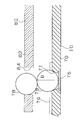
- FIG. 14A is an explanatory view of the dropping of the solder ball onto the connection pad
- FIG. 14B is an explanatory view of the removal of the solder ball by the suction ball removing cylinder.
- FIG. 15A, FIG. 15B, and FIG. 15C are explanatory diagrams of the manufacturing process of the multilayer printed wiring board. It is sectional drawing of a multilayer printed wiring board. It is sectional drawing which shows the state which attached the IC chip to the multilayer printed wiring board shown in FIG. 16, and mounted in the daughter board. It is a top view of the multilayer printed wiring board for multi-piece taking. It is explanatory drawing of the fall of a solder ball when the height of a solder ball is higher than a mask.
Abstract
【課題】 半田ボールを接続パッドへ確実に搭載することができる半田ボール搭載方法を提供する。 【解決手段】 スペーサ86とプリント配線板10との接触部分を避けて、各接続パッド群75gに対してフラックス79を塗布する。このため、スペーサ86にフラックスが付くことが無いので、マスクをプリント配線板から外す際に、プリント配線板を反らせてソルダーレジスト層70を傷つけることが無い。また、スペーサ86を用いて半田ボール78とマスク80上面の高さと一致させることにより、電極パッド75に対して1個ずつの半田ボールを確実に搭載することができ、半田ボールの未搭載、複数個の半田ボールを搭載することによる不良発生の確率を低減することができる。
Description
本発明は、半田バンプとなる半田ボールをプリント配線板に搭載するための半田ボール搭載方法に関するものである。
プリント配線板とICチップとの電気接続のために半田バンプが用いられている。半田バンプは、以下の工程により形成されている。
(1)プリント配線板に形成された接続パッドにフラックスを印刷する工程。
(2)フラックスの印刷された接続パッドに、半田ボールを搭載する工程。
(3)リフローを行い半田ボールから半田バンプを形成する工程。
(1)プリント配線板に形成された接続パッドにフラックスを印刷する工程。
(2)フラックスの印刷された接続パッドに、半田ボールを搭載する工程。
(3)リフローを行い半田ボールから半田バンプを形成する工程。
上述した半田ボールを被搭載体に搭載する工程では、例えば、特許文献1に示されていように、半田ボールを被搭載体に落下させるための開口を備えるマスクが用いられる。引用文献1のマスクにおいては、複数の突起部よりスペーサが形成されている。そして、実際に被搭載体に半田ボールを搭載する際には、隣接する電極部間に突起部が配置されるように、マスクを被搭載体に対して位置あわせする。
特開2006-324618号
ここで、引用文献1においては、フラックスがマスク(スペーサ)に付着しないように電極部にのみ局所的にフラックスを塗布する必要がある。しかしながら、プロセスの簡略化のためには、電極部の形成領域に対してフラックスを一括に塗布することが好ましい。その場合、引用文献1に記載のマスクを使用した場合には、突起部の先端にフラックスが付着してしまい、マスクを基板から取り外し難くなる。さらに、マスクを取り外す際の応力により基板が反ってしまう可能性がある。加えて、マスクを基板から取り外すときには、その際の反動により半田ボールが電極部からずれてしまう可能性もある。
本発明の目的は半田ボールを接続パッドへ確実に搭載することができる半田ボール搭載方法を提供することにある。
上記目的を達成するため、請求項1の発明は、半田バンプとなる半田ボールをプリント配線板の接続パッドに搭載するための半田ボール搭載方法であって:
前記プリント配線板の接続パッドの表面にフラックスを塗布する工程と;
前記接続パッドに対応する複数の開口からなる開口群を有するマスク本体と、前記開口群を露出させる開口部を有するスペーサとからなるマスクを用意する工程と、
前記マスク本体の開口が前記接続パッドに対向するように前記マスクをプリント配線板に対して位置決めする工程と;
前記マスク上に半田ボールを供給し、前記マスク本体の開口を介して半田ボールを前記接続パッドへ落下させる工程と;を備えることを技術的特徴とする。
前記プリント配線板の接続パッドの表面にフラックスを塗布する工程と;
前記接続パッドに対応する複数の開口からなる開口群を有するマスク本体と、前記開口群を露出させる開口部を有するスペーサとからなるマスクを用意する工程と、
前記マスク本体の開口が前記接続パッドに対向するように前記マスクをプリント配線板に対して位置決めする工程と;
前記マスク上に半田ボールを供給し、前記マスク本体の開口を介して半田ボールを前記接続パッドへ落下させる工程と;を備えることを技術的特徴とする。
本願発明に係る半田ボール搭載方法では、プリント配線板の接続パッド形成領域にフラックスを一括して塗布することができ、各接続パッドに対してそれぞれ局所的にフラックスを塗布する場合と比較して製造プロセスの簡略化を図ることができる。また、フラックスの未塗布の接続パッドが生じないため、各接続パッドに確実に半田ボールを搭載することができる。
更に、スペーサをマスク本体と一体で形成することで、マスクの高さを厳密に制御することができ、半田ボールとマスク上面の高さとを一致させ易くなる。これにより、接続パッドに対して1個ずつの半田ボールを確実に搭載することができ、半田ボールの未搭載、複数個の半田ボールの搭載による不良発生の確率を低減することができる。
[第1実施形態]
第1実施形態の半田ボール搭載方法に係る半田ボールをプリント配線板に搭載するためのマスクについて、図1~図7を参照して説明する。
図3は、第1実施形態に係るマスクにより半田ボールを搭載するシートサイズのプリント配線板10を示している。このシートサイズのプリント配線板10は、例えば4×4のピースサイズのプリント配線板10Rを製造するための多数個取り用のものである。図中で鎖線Zに沿って裁断され16個の個片のプリント配線板10Rが製造される。各プリント配線板10Rの中央部には、半田ボールが搭載される接続パッド75が複数形成されてなる接続パッド形成領域75gが設けられている。なお、ここでいう接続パッド形成領域とは、プリント配線板の接続パッドの全てを含む領域のうち最小面積の特定領域を意味する。
図1は、図3に示すプリント配線板に半田ボールを搭載するための第1実施形態に係るマスク80の裏面図である。
マスク80は、プリント配線板10の接続パッド75に対応する開口84からなる開口群84gの形成されたマスク本体82と、開口群84gを露出させる開口部86aの形成されたスペーサ86とから成る。マスク本体82とスペーサ86とは一体に構成されている。なお、ここでいう「一体的に」とは、双方が同じプロセスで形成されているものの他、同じ物質のもの同士、又はそれぞれ異なるもの同士が別途固着されているものも含む。図2は、マスク本体82とスペーサ86とを分離して示し、図2(A)はマスク本体82の平面図であり、図2(B)はスペーサ86の平面図である。
マスク80は、プリント配線板10の接続パッド75に対応する開口84からなる開口群84gの形成されたマスク本体82と、開口群84gを露出させる開口部86aの形成されたスペーサ86とから成る。マスク本体82とスペーサ86とは一体に構成されている。なお、ここでいう「一体的に」とは、双方が同じプロセスで形成されているものの他、同じ物質のもの同士、又はそれぞれ異なるもの同士が別途固着されているものも含む。図2は、マスク本体82とスペーサ86とを分離して示し、図2(A)はマスク本体82の平面図であり、図2(B)はスペーサ86の平面図である。
図4(A)は、図1中のA-A断面に相当し、プリント配線板10上にマスク80を載置した状態を示し、図4(B)は、図4(A)中の円bで示す部位を拡大して示す。
プリント配線板10の表面にはソルダーレジスト層70が形成され、該ソルダーレジスト層70に形成された開口71から接続パッド75が露出している。そして、プリント配線板10の接続パッド形成領域75g全体には、フラックス79が塗布されている。このフラックスの塗布領域は、スペーサの開口部よりも小さい。即ち、プリント配線板10のうち、スペーサ86との当接部位を避けるように、接続パッド形成領域75gにフラックス79が塗布されている。
プリント配線板10の表面にはソルダーレジスト層70が形成され、該ソルダーレジスト層70に形成された開口71から接続パッド75が露出している。そして、プリント配線板10の接続パッド形成領域75g全体には、フラックス79が塗布されている。このフラックスの塗布領域は、スペーサの開口部よりも小さい。即ち、プリント配線板10のうち、スペーサ86との当接部位を避けるように、接続パッド形成領域75gにフラックス79が塗布されている。
第1実施形態では、フラックス79の塗布は、スペーサ86とプリント配線板10との接触部分を避けて、接続パッド形成領域75gに対して行う。このため、スペーサ86にフラックスが付くことが無いので、マスクをプリント配線板から外す際の、プリント配線板の反りや、接続パッドに対する半田ボールのずれ、ソルダーレジスト層70の損傷といった不具合は生じない。
図4(B)に示すように、マスク80の厚みは、接続パッド75に半田ボール78が搭載された状態で、マスク80の上面と、半田ボール78の頂部の高さがほぼ揃うように設定さえている。例えば、半田ボール78の径B(70μm)に対して、マスク本体82の厚みh1が25μm、スペーサ86の厚みh2が30μm、接続パッド75上面からのソルダーレジスト層の厚みh3が15μmに設定される。なお、ここでいう「半田ボールの頂部」とは、半田ボール表面のうち、最も高さの高い箇所を意味する。
第1実施形態の半田ボール搭載方法では、半田ボール78とマスク80上面の高さと一致させることにより、電極パッド75に対して所定量の(1個ずつ)の半田ボールを確実に搭載することができ、半田ボールの未搭載、複数個の半田ボールを搭載することによる不良発生の確率を低減することができる。一方、図19のように、半田ボール78の高さよりもマスク80上面の高さが高い場合、接続パッド上に搭載された半田ボール上に、マスク本体の開口を介して他の半田ボールが搭載されてしまう。このように半田ボールがマスク80上面から突出してしまう場合、他の接続パッド上に半田ボールを搭載する際の障害となり好ましくない。さらに、この状態でリフローされた際には、所定外に体積の大きな半田バンプとなってしまい、歩留まりの低下を招く。
なお、マスク本体の開口の開口径は、半田ボールの径の1.2~1.5倍であることが望ましい。即ち、例えば70μm径の半田ボールを使用する際には、開口径は84~105μmであることが好適である。これにより、接続パッドに確実に半田ボールを一個ずつ搭載することができる。ここで、1.2倍未満では、接続パッドへの未搭載が生じる。他方、1.5倍を超えると複数の半田ボールを接続パッドに搭載する確率が上昇する。
図7(A)は、第1実施形態のマスク80による半田ボールの搭載の説明図である。
マスク80の上方に、該マスクに対向する開口部24Aを備える筒部材24を位置させ、該筒部材24で空気を吸引することで、当該筒部材24直下のマスク上に半田ボール78を集合させ、筒部材24をマスク80に対して水平方向に相対的に移動させることで、マスク80の上に集合させた半田ボール78を移動させ、半田ボール78を接続パッド75へ落下させる。図7(B)は、第1実施形態の改変例を示している。図7(A)では筒部材24で空気を吸引した。これに対して、改変例では、筒部材24から空気を吹き出し、半田ボール78を送って、半田ボール78を接続パッド75へ落下させる。
マスク80の上方に、該マスクに対向する開口部24Aを備える筒部材24を位置させ、該筒部材24で空気を吸引することで、当該筒部材24直下のマスク上に半田ボール78を集合させ、筒部材24をマスク80に対して水平方向に相対的に移動させることで、マスク80の上に集合させた半田ボール78を移動させ、半田ボール78を接続パッド75へ落下させる。図7(B)は、第1実施形態の改変例を示している。図7(A)では筒部材24で空気を吸引した。これに対して、改変例では、筒部材24から空気を吹き出し、半田ボール78を送って、半田ボール78を接続パッド75へ落下させる。
第1実施形態の半田ボール搭載方法によれば、マスク80の上方に筒部材24を位置させ、該筒部材24の開口部から空気を吸引することで半田ボール78を集合させ、筒部材24を水平方向に移動させることで、集合させた半田ボール78をマスク80上を移動させ、マスクの開口84を介して、半田ボール78をプリント配線板10の接続パッド75へ落下させる。このため、微細な半田ボールをプリント配線板の全ての接続パッドへ確実に搭載させることができる。また、半田ボールを非接触で移動させるため、スキージを用いる場合とは異なり、半田ボールに傷を付けることなく接続パッドに搭載でき、半田バンプの高さを均一にすることができる。更に、ビルドアップ多層配線板の様に、表面に起伏の多いプリント配線板でも半田ボールを接続パッドに適切に載置させることができる。
第1実施形態では、スペーサ86の開口部86aに対応させ設けられたマスク本体82の開口群84gの形成された部位が、スペーサ86により4方から支持されるため撓み難く、マスク本体82とプリント配線板10との距離を一定にできる。特に、筒部材24で空気を吸引しても、スペーサ86によりマスク80とプリント配線板10との隙間を通る空気の流れが遮断され、マスク本体がマスク下方から開口群を通る気流により浮き上がることが無く、マスク本体とプリント配線板との距離を常に一定に保つことができる。
第1実施形態のマスク80の製造方法について図5を参照して説明する。
表面処置を施したSUS板200の上に、マスクの開口84を形成するためのめっきレジスト202を形成する(図5(A))。この状態で、ニッケル合金電解めっきにより開口84を備えるマスク本体82を形成する(図5(B))。次に、マスク本体82の上に、スペーサの開口部と成るめっきレジスト204を形成する(図5(C))。次いで、ニッケル合金電解めっきにより開口部86aを備えるスペーサ86を形成する(図5(D))。そして、所定の溶液により、めっきレジスト202及びめっきレジスト204を溶解した後、SUS板200からスペーサ86及びマスク本体82から成るマスク80を剥離する(図5(E))。このように、めっきでスペーサ86とマスク本体82とを一体に形成することで、正確に厚みを調整することができる。
表面処置を施したSUS板200の上に、マスクの開口84を形成するためのめっきレジスト202を形成する(図5(A))。この状態で、ニッケル合金電解めっきにより開口84を備えるマスク本体82を形成する(図5(B))。次に、マスク本体82の上に、スペーサの開口部と成るめっきレジスト204を形成する(図5(C))。次いで、ニッケル合金電解めっきにより開口部86aを備えるスペーサ86を形成する(図5(D))。そして、所定の溶液により、めっきレジスト202及びめっきレジスト204を溶解した後、SUS板200からスペーサ86及びマスク本体82から成るマスク80を剥離する(図5(E))。このように、めっきでスペーサ86とマスク本体82とを一体に形成することで、正確に厚みを調整することができる。
第1実施形態では、スペーサ86とマスク本体82とを一体に形成したが、別体で形成したスペーサとマスク本体とを例えば超音波接合または接着剤により貼り付けることも可能である。更に、スペーサとマスク本体とを異なる素材で形成しても良い。例えば、マスク本体を金属で形成し、スペーサを樹脂で形成することも可能である。
該マスクの支持具への取り付けについて図6を参照して説明する。
支持具は、図6(A)に示すように、枠体210にテンションが均一に加えられたナイロン布220が貼られた物を用いる。図6(B)に示すように、このナイロン布220の中央に、マスク80を接着剤222を介して貼り付ける。この接着剤222は、マスク本体82の外縁であって、スペーサ86よりも外側に塗布する。最後に、図6(C)に示すように、接着剤222の内側のナイロン布220に開口220Aを形成することで、ナイロン布220の均一なテンションをマスク80に加える。
支持具は、図6(A)に示すように、枠体210にテンションが均一に加えられたナイロン布220が貼られた物を用いる。図6(B)に示すように、このナイロン布220の中央に、マスク80を接着剤222を介して貼り付ける。この接着剤222は、マスク本体82の外縁であって、スペーサ86よりも外側に塗布する。最後に、図6(C)に示すように、接着剤222の内側のナイロン布220に開口220Aを形成することで、ナイロン布220の均一なテンションをマスク80に加える。
第1実施形態では、図6(B)及び図1に示すようにマスク本体82の外縁は、スペーサ86の外縁よりも延在している。スペーサ86の外縁よりも延在しているマスク本体82の外縁にテンションを加えることで、マスク本体において、スペーサが存在している部分及びスペーサの開口部に位置する部分に均一のテンションが加わるようになる。すなわち、マスク本体の全体にわたって均一のテンションが加わるようになる。その結果、テンション差による撓みが抑制され、マスク本体の高さを厳密に制御することができ、半田ボールとマスク上面の高さとを一致させ易くなる。
[第2実施形態]
第2実施形態に係るマスクについて、該マスクの裏面を示す図8を参照して説明する。
第1実施形態では、スペーサ86の開口部86aをマスク本体の開口群84gごとに各々形成した。これに対して、第2実施形態では、マスク本体の複数の開口群84gを一括して露出させるような開口部86aをスペーサ86に形成している。
第2実施形態に係るマスクについて、該マスクの裏面を示す図8を参照して説明する。
第1実施形態では、スペーサ86の開口部86aをマスク本体の開口群84gごとに各々形成した。これに対して、第2実施形態では、マスク本体の複数の開口群84gを一括して露出させるような開口部86aをスペーサ86に形成している。
[第3実施形態]
第3実施形態の半田ボール搭載方法について図9(A)を参照して説明する。第1実施形態では、気流により半田ボールを移送した。これに対して、第3実施形態では、ブラシ110により接続パッド上に半田ボールを搭載する。
第3実施形態の半田ボール搭載方法について図9(A)を参照して説明する。第1実施形態では、気流により半田ボールを移送した。これに対して、第3実施形態では、ブラシ110により接続パッド上に半田ボールを搭載する。
[第3実施形態の改変例]
第3実施形態の改変例に係る半田ボール搭載方法について図9(B)を参照して説明する。第3実施形態の改変例では、可撓性を備えるスキージ112により接続パッド上に半田ボールを搭載する。
第3実施形態の改変例に係る半田ボール搭載方法について図9(B)を参照して説明する。第3実施形態の改変例では、可撓性を備えるスキージ112により接続パッド上に半田ボールを搭載する。
[第4実施形態]
第4実施形態の半田ボール搭載方法について図10(A)を参照して説明する。第1実施形態では、気流により半田ボールを移送した。これに対して、第4実施形態では、マスク80及びプリント配線板に振動を与えることで接続パッド上に半田ボールを搭載する。
第4実施形態の半田ボール搭載方法について図10(A)を参照して説明する。第1実施形態では、気流により半田ボールを移送した。これに対して、第4実施形態では、マスク80及びプリント配線板に振動を与えることで接続パッド上に半田ボールを搭載する。
[第4実施形態の改変例]
第4実施形態の改変例に係る半田ボール搭載方法について図10(B)を参照して説明する。第4実施形態の改変例では、マスク80及びプリント配線板を傾動させることで半田ボールを搬送する。
第4実施形態の改変例に係る半田ボール搭載方法について図10(B)を参照して説明する。第4実施形態の改変例では、マスク80及びプリント配線板を傾動させることで半田ボールを搬送する。
[第1実施例]
引き続き、本発明の第1実施例について図11~図17を参照して説明する。
先ず、本発明の第1実施例に係る半田ボール搭載方法を用いて製造する多層プリント配線板10の構成について、図16及び図17を参照して説明する。図16は、該多層プリント配線板10の断面図を、図17は、図16に示す多層プリント配線板10にICチップ90を取り付け、ドータボード94へ載置した状態を示している。図16に示すように多層プリント配線板10では、コア基板30の両面に導体回路34が形成されている。コア基板30の表面と裏面とはスルーホール36を介して接続されている。
引き続き、本発明の第1実施例について図11~図17を参照して説明する。
先ず、本発明の第1実施例に係る半田ボール搭載方法を用いて製造する多層プリント配線板10の構成について、図16及び図17を参照して説明する。図16は、該多層プリント配線板10の断面図を、図17は、図16に示す多層プリント配線板10にICチップ90を取り付け、ドータボード94へ載置した状態を示している。図16に示すように多層プリント配線板10では、コア基板30の両面に導体回路34が形成されている。コア基板30の表面と裏面とはスルーホール36を介して接続されている。
更に、コア基板30の導体回路34の上に層間樹脂絶縁層50を介して導体回路層を形成する導体回路58が形成されている。導体回路58は、バイアホール60を介して導体回路34と接続されている。導体回路58の上に層間樹脂絶縁層150を介して導体回路158が形成されている。導体回路158は、層間樹脂絶縁層150に形成されたバイアホール160を介して導体回路58に接続されている。
バイアホール160、導体回路158の上層にはソルダーレジスト層70が形成されており、該ソルダーレジスト層70の開口71にニッケルめっき層72及び金めっき層74を設けることで、接続パッド75が形成されている。上面の接続パッド75上には半田バンプ78Uが、下面の接続パッド75上には半田バンプ78Dが形成されている。
図17中に示すように、多層プリント配線板10の上面側の半田バンプ78Uは、ICチップ90の電極92へ接続される。一方、下側の半田バンプ78Dは、ドータボード94のランド96へ接続されている。
図18は、多数個取り用(シートサイズ)の多層プリント配線板10Aの平面図である。多層プリント配線板10Aは、マトリクス状に接続パッド75が配列された接続パッド形成領域75gを備える個々の(ピースサイズの)多層プリント配線板10を、図中の一点鎖線で切断することで切り分ける。図15は、多数個取り用の多層プリント配線板10Aに半田バンプを形成する工程の説明図であり、図18中のY1-Y1断面図に相当する。図15(A)に示すようにソルダーレジスト層70の開口71を含む表面、及び接続パッド75の表面にフラックス79を一括して印刷する。図15(B)に示すように多層プリント配線板10Aの上側の接続パッド75上に後述する半田ボール搭載装置を用いて微少な半田ボール78s(例えば日立金属(株)社製、直径40μmΦ以上、200μmΦ未満)を搭載する。この場合、直径40μmΦ未満では半田ボールが軽すぎるため接続パッド上に落下させるのが困難となる。一方、直径200μmを越えると逆に重すぎるため筒部材内に半田ボールを集合させることができず、半田ボールが載っていない接続パッドが存在するようになる。本発明では、直径40μmΦ以上直径200μmΦ未満の半田ボールを使う意義が高い。この範囲では、ソルダーレジスト層70の開口71の径の微小化に伴うファイン化に有利である。また、吸着ヘッドで半田ボールを吸着して接続パッド上に半田ボールを搭載する方法では、半田ボールが小さいので吸着するのが困難になるため、実施例の方法の優位性が明らかになる。
その後、図15(C)に示すように多層プリント配線板10Aの下側の接続パッド75上に、従来技術(例えば、特許1975429号)に係る吸着ヘッドで通常径(直径250μm)の半田ボール78Lを吸着して載置する。その後、リフロー炉で過熱し、図16に示すように多層プリント配線板10Aの上側に60μm以上200μm未満ピッチで半田バンプ78Uを、例えば500~30000個、下側に2mmピッチで半田バンプ78Dを、例えば250個形成する。60μmピッチ未満となると、そのピッチに適した半田ボールを製造するのが困難になる。200μmピッチ以上になると、本方法においても何ら問題なく製造できるが、従来技術の方法でも製造可能である。更に、図17に示すように、多数個取り用の多層プリント配線板10Aを個片の多層プリント配線板10に切り分けてから、リフローにより半田バンプ78Uを介してICチップ90を搭載させた後、ICチップ90を搭載した多層プリント配線板10を、半田バンプ78Dを介してドータボード94へ取り付ける。
図15(B)を参照して上述した多層プリント配線板の接続パッド上に微少(直径200μmΦ未満)な半田ボール78sを搭載する半田ボール搭載装置について、図11を参照して説明する。
図11(A)は、第1実施例の半田ボール搭載方法に係る半田ボール搭載装置の構成を示す構成図であり、図11(B)は、図11(A)の半田ボール搭載装置を矢印B側から見た矢視図である。
図11(A)は、第1実施例の半田ボール搭載方法に係る半田ボール搭載装置の構成を示す構成図であり、図11(B)は、図11(A)の半田ボール搭載装置を矢印B側から見た矢視図である。
半田ボール搭載装置20は、多層プリント配線板10Aを位置決め保持するXYθ吸引テーブル14と、該XYθ吸引テーブル14を昇降する上下移動軸12と、多層プリント配線板の接続パッド75に対応する開口を備えるボール整列用マスク80と、ボール整列用マスク80上を移動する半田ボールを誘導する搭載筒(筒部材)24と、搭載筒24に負圧を与える吸引ボックス26と、余剰の半田ボールを回収するための吸着ボール除去筒61と、該吸着ボール除去筒61に負圧を与える吸引ボックス66と、回収した半田ボールを保持する吸着ボール除去吸引装置68と、ボール整列用マスク80をクランプするマスククランプ44と、搭載筒24及び吸着ボール除去筒61をX方向へ送るX方向移動軸40と、X方向移動軸40を支持する移動軸支持ガイド42と、多層プリント配線板10を撮像するためのアライメントカメラ46と、搭載筒24下にある半田ボールの残量を検出する残量検出センサ18と、残量検出センサ18により検出された残量に基づき半田ボールを搭載筒24側へ供給する半田ボール供給装置22と、を備える。図11に示す半田ボール搭載装置20では、搭載筒24及び吸着ボール除去筒61をX方向へ送るX方向移動軸40のみ示したが、Y方向へ送る移動機構を備えることも可能である。なお、X方向、Y方向への送りは、搭載筒24側を固定し、ボール整列用マスク80及びプリント配線板側を送ることも可能である。
図1は、図11に示す半田ボール搭載装置20に用いられるマスク80の裏面図である。
マスク80は、プリント配線板10の接続パッド75に対応する開口84からなる開口群84gの形成されたマスク本体82と、開口群84gを露出させる開口部86aの形成されたスペーサ86とから成り、マスク本体82とスペーサ86とは一体に構成されている。
マスク80は、プリント配線板10の接続パッド75に対応する開口84からなる開口群84gの形成されたマスク本体82と、開口群84gを露出させる開口部86aの形成されたスペーサ86とから成り、マスク本体82とスペーサ86とは一体に構成されている。
図4(A)は、図1中のA-A断面に相当し、プリント配線板10上にマスク80を載置した状態を示し、図4(B)は、図4(A)中の円bで示す部位の拡大図である。
プリント配線板10の表面にはソルダーレジスト層70が形成され、該ソルダーレジスト層70の開口71から露出するように接続パッド75が設けられている。1ピース分の接続パッド75からなる接続パッド形成領域75gには、フラックス79が塗布されている。即ち、本発明においては、スペーサとプリント配線板との接触部分を避けて、フラックスが各接続パッドに塗布される。このフラックスの塗布領域は、スペーサの開口部面積よりも小さい。
プリント配線板10の表面にはソルダーレジスト層70が形成され、該ソルダーレジスト層70の開口71から露出するように接続パッド75が設けられている。1ピース分の接続パッド75からなる接続パッド形成領域75gには、フラックス79が塗布されている。即ち、本発明においては、スペーサとプリント配線板との接触部分を避けて、フラックスが各接続パッドに塗布される。このフラックスの塗布領域は、スペーサの開口部面積よりも小さい。
このため、スペーサ86にフラックスが付くことが無いので、マスクをプリント配線板から外す際に、プリント配線板を反らせたり、ソルダーレジスト層70を傷つけたりすることがほとんど無い。
また、半田ボールを前記接続パッドへ落下させたときには、図4(B)に示すように、半田ボールの頂部は、マスク本体の表面と略同一高さに位置する。この第1実施例の半田ボール搭載方法では、半田ボール78とマスク80上面の高さと一致させることにより、電極パッド75に対して所定量の(1個ずつの)半田ボールを確実に搭載することができ、半田ボールの未搭載や、複数個の半田ボールが搭載されることによる不良発生の確率を低減することができる。
第1実施例では、搭載筒24がSUSステンレス、Ni、Cu等の導電性金属で構成され、半田ボール搭載装置20側にアースされている。ここで、半田ボールをボール整列用マスク80上に移動させて送る際に、相互の衝突により半田ボールが帯電しても、小径で軽量な半田ボールが静電気により搭載筒24へ付着することがほとんどない。これにより、半田ボールをプリント配線板に確実に搭載することができる。
図18の平面図に示すようにシートサイズの多層プリント配線板10Aの上に、半田ボール搭載装置20の搭載筒24(図示しないが吸着ボール除去筒61も搭載筒と同様に並べられている)は、個々の接続パッド形成領域75gに対応させてY方向へ複数並べてある。なお、ここでは、1の接続パッド形成領域75gに1の搭載筒24を対応させたが、搭載筒24を複数の接続パッド形成領域75gに対応した大きさにしてもよい。ここで、Y方向は便宜的であり、X方向に並べても良い。
また、図11に示すXYθ吸引テーブル14は、半田ボールの搭載される多層プリント配線板10を位置決め、吸着、保持、補正する。アライメントカメラ46は、XYθ吸引テーブル14上の多層プリント配線板10のアライメントマークを検出し、検出された位置に基づき、多層プリント配線板10とボール整列用マスク80との位置が調整される。残量検出センサ18は光学的な手法により半田ボールの残量を検出する。
また、図11に示すXYθ吸引テーブル14は、半田ボールの搭載される多層プリント配線板10を位置決め、吸着、保持、補正する。アライメントカメラ46は、XYθ吸引テーブル14上の多層プリント配線板10のアライメントマークを検出し、検出された位置に基づき、多層プリント配線板10とボール整列用マスク80との位置が調整される。残量検出センサ18は光学的な手法により半田ボールの残量を検出する。
引き続き、半田ボール搭載装置20による半田ボールの搭載工程について図12~図14を参照して説明する。
(1)多層プリント配線板の位置認識、補正
図12(A)に示すように多数個取り用の多層プリント配線板10Aのアライメントマーク34Mをアライメントカメラ46により認識し、ボール整列用マスク80に対して多層プリント配線板10Aの位置をXYθ吸引テーブル14によって補正する。即ち、ボール整列用マスク80の開口84がそれぞれ多層プリント配線板10Aの接続パッド75に対応するように位置調整する。
(1)多層プリント配線板の位置認識、補正
図12(A)に示すように多数個取り用の多層プリント配線板10Aのアライメントマーク34Mをアライメントカメラ46により認識し、ボール整列用マスク80に対して多層プリント配線板10Aの位置をXYθ吸引テーブル14によって補正する。即ち、ボール整列用マスク80の開口84がそれぞれ多層プリント配線板10Aの接続パッド75に対応するように位置調整する。
(2)半田ボール供給
図12(B)に示すように半田ボール供給装置22から半田ボール78sを搭載筒24側へ定量供給する。なお、予め搭載筒内に供給しておいても良い。
図12(B)に示すように半田ボール供給装置22から半田ボール78sを搭載筒24側へ定量供給する。なお、予め搭載筒内に供給しておいても良い。
(3)半田ボール搭載
図13(A)に示すように、ボール整列用マスク80の上方に、該ボール整列用マスクとの所定のクリアランス(例えば、ボール径の0.5~4倍)を保ち搭載筒24を位置させ、吸引部24bから空気を吸引することで、搭載筒とボール整列用マスクの隙間の流速を5m/sec~35m/secにして、当該搭載筒24の開口部24A直下のボール整列用マスク80上に半田ボール78sを集合させる。
図13(A)に示すように、ボール整列用マスク80の上方に、該ボール整列用マスクとの所定のクリアランス(例えば、ボール径の0.5~4倍)を保ち搭載筒24を位置させ、吸引部24bから空気を吸引することで、搭載筒とボール整列用マスクの隙間の流速を5m/sec~35m/secにして、当該搭載筒24の開口部24A直下のボール整列用マスク80上に半田ボール78sを集合させる。
その後、図13(B)、図14(A)及び図18に示すように、図11(B)及び図11(A)に示す多層プリント配線板10AのY軸沿って並べられた搭載筒24を、X方向移動軸40を介してX軸に沿って水平方向へ送る。これにより、ボール整列用マスク80の上に集合させた半田ボール78sを搭載筒24の移動に伴い移動させ、ボール整列用マスク80の開口84を介して、半田ボール78sを多層プリント配線板10Aの接続パッド75へ落下、搭載させて行く。これにより、半田ボール78sが多層プリント配線板10A側の全接続パッド上に順次整列される。
(4)付着半田ボール除去
図14(B)に示すように、搭載筒24により余剰の半田ボール78sをボール整列用マスク80上に開口84の無い位置まで誘導した後、吸着ボール除去筒61により吸引除去する。
図14(B)に示すように、搭載筒24により余剰の半田ボール78sをボール整列用マスク80上に開口84の無い位置まで誘導した後、吸着ボール除去筒61により吸引除去する。
(5)基板取り出し
XYθ吸引テーブル14から多層プリント配線板10Aを取り外す。
XYθ吸引テーブル14から多層プリント配線板10Aを取り外す。
第1実施例の半田ボール搭載方法によれば、ボール整列用マスク80の上方に搭載筒24を位置させ、該搭載筒24の吸引部24B(図12(B)参照)から空気を吸引することで半田ボール78sを集合させる。そして、この状態で搭載筒24を水平方向に移動させることで、集合させた半田ボール78sをボール整列用マスク80の上を移動させ、ボール整列用マスク80の開口84を介して、半田ボール78sを多層プリント配線板10Aの接続パッド75へ落下させる。このため、微細な半田ボール78sを確実に多層プリント配線板10Aの全ての接続パッド75に搭載させることができる。また、半田ボール78sを非接触で移動させるため、スキージを用いる場合とは異なり、半田ボールを傷を付けることなく接続パッド75に搭載でき、半田バンプ78Uの高さを均一にすることができる。このため、IC等の電子部品の実装性、実装後のヒートサイクル試験、高温・高湿試験等の耐環境試験に優れる。更に、製品の平面度に依存しないので、表面に起伏の多いプリント配線板でも半田ボールを接続パッドに適切に載置させることができる。また、微少な半田ボールを確実に接続パッド上に載置することができるので、接続パッドピッチが60~150μmピッチでソルダーレジストの開口径が150μm未満のプリント配線板においても、高さが均一な半田バンプを形成することが可能となる。
更に、吸引力により半田ボールを誘導するため、半田ボールの凝集、付着を防止することができる。更に、搭載筒24の数を調整することで、種々のシートサイズの多層プリント配線板に対応することができる。このため、多品種、少量生産にも柔軟に適用することが可能である。
[第1実施例-1]
(1)プリント配線板の作製
出発材料として両面銅張積層板(例えば、日立化成工業株式会社製 MCL-E-67)を用い、この基板に周知の方法でスルーホール導体及び導体回路を形成した。その後、周知の方法(例えば、2000年6月20日 日刊工業新聞社発行の「ビルドアップ多層プリント配線板」(高木清著)で層間絶縁層と導体回路層とを交互に積層し、最外層の導体回路層において、ICへ電気的に接続するための接続パッドを形成する。次いで、この接続パッドを露出させるような開口(例えば150μmΦ)を有するソルダーレジスト層を形成する。
(1)プリント配線板の作製
出発材料として両面銅張積層板(例えば、日立化成工業株式会社製 MCL-E-67)を用い、この基板に周知の方法でスルーホール導体及び導体回路を形成した。その後、周知の方法(例えば、2000年6月20日 日刊工業新聞社発行の「ビルドアップ多層プリント配線板」(高木清著)で層間絶縁層と導体回路層とを交互に積層し、最外層の導体回路層において、ICへ電気的に接続するための接続パッドを形成する。次いで、この接続パッドを露出させるような開口(例えば150μmΦ)を有するソルダーレジスト層を形成する。
(2)半田ボール搭載
(1)で作製したプリント配線板の接続パッド形成領域に市販のロジン系フラックスを塗布する。その後、上述した本願発明の半田ボール搭載装置の吸着テーブルに搭載し、プリント配線板およびボール整列用マスクのアライメントマークをCCDカメラを用いて認識し、プリント配線板とボール整列用マスクを位置合わせする。ここで、ボール整列用マスクは、裏面にスペーサを備え、プリント配線板の接続パッドに対応した位置に直径110μmの開口を有するNi製のマスクを用いた。ここでは、Ni製のメタルマスクを用いたが、SUS製やポリイミド製のボール整列用マスクを用いることも可能である。尚、ボール整列用マスクに形成する開口径は、使用するボールの径に対して1.2~1.5倍が好ましい。次に、接続パッド形成領域にほぼ対応した大きさ(接続パッド形成領域に対して1.1~4倍)で、高さ200mmのSUS製の搭載筒を半田ボール径の0.5~4倍のクリアランスを保ってメタルマスク(ボール整列用マスク)上に位置させる。そして、その周囲近辺のボール整列用マスク上に、例えばボール直径80μmΦのSn63Pb37半田ボール(日立金属社製)を載せる。なお、第1実施例-1では半田ボールにSn/Pb半田を用いたが、半田ボールの組成はこれに限定されるものではなく、SnとAg、Cu、In、Bi、Zn等の群から選ばれるPbフリー半田であってもよい。
(1)で作製したプリント配線板の接続パッド形成領域に市販のロジン系フラックスを塗布する。その後、上述した本願発明の半田ボール搭載装置の吸着テーブルに搭載し、プリント配線板およびボール整列用マスクのアライメントマークをCCDカメラを用いて認識し、プリント配線板とボール整列用マスクを位置合わせする。ここで、ボール整列用マスクは、裏面にスペーサを備え、プリント配線板の接続パッドに対応した位置に直径110μmの開口を有するNi製のマスクを用いた。ここでは、Ni製のメタルマスクを用いたが、SUS製やポリイミド製のボール整列用マスクを用いることも可能である。尚、ボール整列用マスクに形成する開口径は、使用するボールの径に対して1.2~1.5倍が好ましい。次に、接続パッド形成領域にほぼ対応した大きさ(接続パッド形成領域に対して1.1~4倍)で、高さ200mmのSUS製の搭載筒を半田ボール径の0.5~4倍のクリアランスを保ってメタルマスク(ボール整列用マスク)上に位置させる。そして、その周囲近辺のボール整列用マスク上に、例えばボール直径80μmΦのSn63Pb37半田ボール(日立金属社製)を載せる。なお、第1実施例-1では半田ボールにSn/Pb半田を用いたが、半田ボールの組成はこれに限定されるものではなく、SnとAg、Cu、In、Bi、Zn等の群から選ばれるPbフリー半田であってもよい。
そして、搭載筒上部の吸引部(5~20mmΦ)24B(図12(B)参照)より空気を吸引し、半田ボールを搭載筒内のボール整列用マスク上に集合させた。
その後、搭載筒を移動速度20mm/secで送って半田ボールを移動させ、ボール整列用マスクの開口部から半田ボールを落下させて接続パッド上に半田ボールを搭載した。第1実施例-1では、搭載筒24がSUSステンレス、Ni、Cu等の導電性金属で構成され、半田ボール搭載装置20側にアースされている。次に、ボール整列用マスクの余分な半田ボールを除去したのち、半田ボール整列用マスクとプリント配線板を半田ボール搭載装置から別個に取り外した。そして、接続パッド上に搭載された半田ボールを例えば230℃でリフローすることにより、所定の半田バンプが形成される。
10 プリント配線板
20 半田ボール搭載装置
22 半田ボール供給装置
24 搭載筒(筒部材)
75 接続パッド
75g 接続パッド群
80 ボール整列用マスク
82 マスク本体
84 開口
86 スペーサ
78s 半田ボール
20 半田ボール搭載装置
22 半田ボール供給装置
24 搭載筒(筒部材)
75 接続パッド
75g 接続パッド群
80 ボール整列用マスク
82 マスク本体
84 開口
86 スペーサ
78s 半田ボール
Claims (9)
- 半田バンプとなる半田ボールをプリント配線板の接続パッドに搭載するための半田ボール搭載方法であって:
前記プリント配線板の接続パッドの表面にフラックスを塗布する工程と;
前記接続パッドに対応する複数の開口からなる開口群を有するマスク本体と、前記開口群を露出させる開口部を有するスペーサとからなるマスクを用意する工程と、
前記マスク本体の開口が前記接続パッドに対向するように前記マスクをプリント配線板に対して位置決めする工程と;
前記マスク上に半田ボールを供給し、前記マスク本体の開口を介して半田ボールを前記接続パッドへ落下させる工程と;を備えることを特徴とする半田ボール搭載方法。 - 前記スペーサは、前記マスク本体に一体的に形成されていることを特徴とする請求項1の半田ボール搭載方法。
- 前記半田ボールを前記接続パッドへ落下させたとき、前記半田ボールの頂部は、前記マスク本体の表面と略同一高さに位置することを特徴とする請求項1又は2の半田ボール搭載方法。
- 前記接続パッドの形成領域全体に前記フラックスを塗布することを特徴とする請求項1~請求項3のいずれか1の半田ボール搭載方法。
- 前記フラックスは、前記スペーサとプリント配線板との接触部分を避けて、各接続パッドに塗布されることを特徴とする請求項1~請求項4のいずれか1の半田ボール搭載方法。
- 前記フラックスの塗布領域は、前記スペーサの開口部よりも小さいことを特徴とする請求項1~請求項5のいずれか1の半田ボール搭載方法。
- 前記マスク本体の開口の径は、前記半田ボールの径の1.2~1.5倍であることを特徴とする請求項1~請求項5のいずれか1の半田ボール搭載方法。
- 前記マスク本体の外縁は、前記スペーサの外縁よりも延在していることを特徴とする請求項1~請求項7のいずれか1の半田ボール搭載方法。
- 前記半田ボールを前記接続パッドへ落下させる工程において:
前記マスクの上方に、該マスクに対向する開口部を備える筒部材を位置させ、該筒部材で空気を吸引することで、当該筒部材直下のマスク上に半田ボールを集合させ、前記筒部材を前記マスクに対して水平方向に移動させることで、前記マスクの上に集合させた半田ボールを移動させ、前記半田ボールを前記接続パッドへ落下させることを特徴とする請求項1又は請求項2の半田ボール搭載方法。
Priority Applications (3)
| Application Number | Priority Date | Filing Date | Title |
|---|---|---|---|
| CN2008800132588A CN101683001B (zh) | 2008-05-30 | 2008-09-24 | 焊锡球搭载方法 |
| JP2009529438A JPWO2009144846A1 (ja) | 2008-05-30 | 2008-09-24 | 半田ボール搭載方法 |
| EP08811125A EP2157841A4 (en) | 2008-05-30 | 2008-09-24 | MOUNTING DEVICE FOR A SOLDERING BALL |
Applications Claiming Priority (2)
| Application Number | Priority Date | Filing Date | Title |
|---|---|---|---|
| US5747908P | 2008-05-30 | 2008-05-30 | |
| US61/057,479 | 2008-05-30 |
Publications (1)
| Publication Number | Publication Date |
|---|---|
| WO2009144846A1 true WO2009144846A1 (ja) | 2009-12-03 |
Family
ID=41376739
Family Applications (1)
| Application Number | Title | Priority Date | Filing Date |
|---|---|---|---|
| PCT/JP2008/067170 WO2009144846A1 (ja) | 2008-05-30 | 2008-09-24 | 半田ボール搭載方法 |
Country Status (5)
| Country | Link |
|---|---|
| US (3) | US8157157B2 (ja) |
| EP (1) | EP2157841A4 (ja) |
| JP (1) | JPWO2009144846A1 (ja) |
| CN (1) | CN101683001B (ja) |
| WO (1) | WO2009144846A1 (ja) |
Cited By (3)
| Publication number | Priority date | Publication date | Assignee | Title |
|---|---|---|---|---|
| JP2012074595A (ja) * | 2010-09-29 | 2012-04-12 | Toppan Printing Co Ltd | 半導体パッケージの製造方法 |
| KR20150001205A (ko) * | 2013-06-26 | 2015-01-06 | 삼성전자주식회사 | 솔더 볼 탑재 장치 |
| JP2015225922A (ja) * | 2014-05-27 | 2015-12-14 | 新光電気工業株式会社 | ボール搭載用マスクおよびボール搭載方法 |
Families Citing this family (14)
| Publication number | Priority date | Publication date | Assignee | Title |
|---|---|---|---|---|
| JP5021473B2 (ja) * | 2005-06-30 | 2012-09-05 | イビデン株式会社 | プリント配線板の製造方法 |
| TW200746964A (en) * | 2006-01-27 | 2007-12-16 | Ibiden Co Ltd | Method of manufacturing printed wiring board |
| US7780063B2 (en) * | 2008-05-15 | 2010-08-24 | International Business Machines Corporation | Techniques for arranging solder balls and forming bumps |
| TW201025467A (en) * | 2008-12-25 | 2010-07-01 | United Test Ct Inc | Ball implantation method and ball implantation system applying the method |
| US8937008B2 (en) * | 2011-12-29 | 2015-01-20 | Stmicroelectronics Pte Ltd. | Apparatus and method for placing solder balls |
| CN103797901B (zh) * | 2012-08-10 | 2017-04-12 | 松下知识产权经营株式会社 | 部件安装基板的制造方法及制造系统 |
| KR102029077B1 (ko) | 2013-02-04 | 2019-10-07 | 삼성전자주식회사 | 패키지의 외부접속단자 형성 방법 및 이를 수행하기 위한 장치 |
| JP6320066B2 (ja) * | 2014-02-13 | 2018-05-09 | イビデン株式会社 | ボール搭載用マスクおよびボール搭載装置 |
| CN103785922A (zh) * | 2014-03-04 | 2014-05-14 | 昆山泰威尔电子科技有限公司 | 一种用于焊接锡球的挡盘 |
| JP5838436B1 (ja) * | 2015-04-13 | 2016-01-06 | 株式会社プロセス・ラボ・ミクロン | 導電性ボール定置用マスク、及びその製造方法 |
| KR102528016B1 (ko) * | 2018-10-05 | 2023-05-02 | 삼성전자주식회사 | 솔더 부재 실장 방법 및 시스템 |
| KR102078936B1 (ko) * | 2018-11-07 | 2020-02-19 | 주식회사 프로텍 | 도전성 볼 탑재 방법 |
| KR102078935B1 (ko) * | 2018-11-07 | 2020-02-19 | 주식회사 프로텍 | 도전성 볼 탑재 장치 |
| CN114980558B (zh) * | 2022-05-13 | 2023-11-14 | 中国电子科技集团公司第二十四研究所 | 一种bga植球方法及植球装置 |
Citations (2)
| Publication number | Priority date | Publication date | Assignee | Title |
|---|---|---|---|---|
| JP2006324618A (ja) * | 2005-04-20 | 2006-11-30 | Kyushu Hitachi Maxell Ltd | 導電性ボール配列用マスク及びその製造方法 |
| WO2007004657A1 (ja) * | 2005-06-30 | 2007-01-11 | Ibiden Co., Ltd. | プリント配線板 |
Family Cites Families (11)
| Publication number | Priority date | Publication date | Assignee | Title |
|---|---|---|---|---|
| US4324815A (en) * | 1978-01-24 | 1982-04-13 | Mitani Electronics Industry Corp. | Screen-printing mask and method |
| JPH0795554B2 (ja) * | 1987-09-14 | 1995-10-11 | 株式会社日立製作所 | はんだ球整列装置 |
| JPH10126046A (ja) * | 1996-10-18 | 1998-05-15 | Oki Electric Ind Co Ltd | ボール・グリッド・アレイの製造装置 |
| US6869008B2 (en) | 1998-05-29 | 2005-03-22 | Hitachi, Ltd. | Method of forming bumps |
| US6547097B1 (en) * | 1999-05-27 | 2003-04-15 | The Knight Group Llc | Dispensing apparatus and method |
| SG99331A1 (en) * | 2000-01-13 | 2003-10-27 | Hitachi Ltd | Method of producing electronic part with bumps and method of producing elctronic part |
| TWI285524B (en) * | 2003-03-10 | 2007-08-11 | Hitachi Metals Ltd | Method and apparatus for carrying electric conductive ball |
| JPWO2006043377A1 (ja) * | 2004-10-19 | 2008-05-22 | 千住金属工業株式会社 | はんだバンプ形成用シートとその製造方法 |
| JP5021473B2 (ja) * | 2005-06-30 | 2012-09-05 | イビデン株式会社 | プリント配線板の製造方法 |
| US7472473B2 (en) * | 2006-04-26 | 2009-01-06 | Ibiden Co., Ltd. | Solder ball loading apparatus |
| JP4219951B2 (ja) * | 2006-10-25 | 2009-02-04 | 新光電気工業株式会社 | はんだボール搭載方法及びはんだボール搭載基板の製造方法 |
-
2008
- 2008-09-24 EP EP08811125A patent/EP2157841A4/en not_active Withdrawn
- 2008-09-24 CN CN2008800132588A patent/CN101683001B/zh not_active Expired - Fee Related
- 2008-09-24 WO PCT/JP2008/067170 patent/WO2009144846A1/ja active Application Filing
- 2008-09-24 JP JP2009529438A patent/JPWO2009144846A1/ja active Pending
-
2009
- 2009-01-07 US US12/349,748 patent/US8157157B2/en active Active
-
2011
- 2011-12-09 US US13/315,843 patent/US20120080504A1/en not_active Abandoned
- 2011-12-09 US US13/315,972 patent/US8448838B2/en active Active
Patent Citations (2)
| Publication number | Priority date | Publication date | Assignee | Title |
|---|---|---|---|---|
| JP2006324618A (ja) * | 2005-04-20 | 2006-11-30 | Kyushu Hitachi Maxell Ltd | 導電性ボール配列用マスク及びその製造方法 |
| WO2007004657A1 (ja) * | 2005-06-30 | 2007-01-11 | Ibiden Co., Ltd. | プリント配線板 |
Non-Patent Citations (1)
| Title |
|---|
| See also references of EP2157841A4 * |
Cited By (4)
| Publication number | Priority date | Publication date | Assignee | Title |
|---|---|---|---|---|
| JP2012074595A (ja) * | 2010-09-29 | 2012-04-12 | Toppan Printing Co Ltd | 半導体パッケージの製造方法 |
| KR20150001205A (ko) * | 2013-06-26 | 2015-01-06 | 삼성전자주식회사 | 솔더 볼 탑재 장치 |
| KR102100867B1 (ko) | 2013-06-26 | 2020-04-14 | 삼성전자주식회사 | 솔더 볼 탑재 장치 |
| JP2015225922A (ja) * | 2014-05-27 | 2015-12-14 | 新光電気工業株式会社 | ボール搭載用マスクおよびボール搭載方法 |
Also Published As
| Publication number | Publication date |
|---|---|
| US20090294516A1 (en) | 2009-12-03 |
| CN101683001B (zh) | 2012-01-04 |
| US8157157B2 (en) | 2012-04-17 |
| EP2157841A1 (en) | 2010-02-24 |
| US20120080505A1 (en) | 2012-04-05 |
| JPWO2009144846A1 (ja) | 2011-10-06 |
| CN101683001A (zh) | 2010-03-24 |
| US20120080504A1 (en) | 2012-04-05 |
| US8448838B2 (en) | 2013-05-28 |
| EP2157841A4 (en) | 2011-11-02 |
Similar Documents
| Publication | Publication Date | Title |
|---|---|---|
| WO2009144846A1 (ja) | 半田ボール搭載方法 | |
| JP4647007B2 (ja) | 半田ボール搭載装置 | |
| JP5021472B2 (ja) | プリント配線板の製造方法 | |
| JP5021473B2 (ja) | プリント配線板の製造方法 | |
| WO2006013742A1 (ja) | 半田ボール搭載方法及び半田ボール搭載装置 | |
| JP5056491B2 (ja) | 半田ボール搭載装置 | |
| JP4592762B2 (ja) | 半田ボール搭載方法及び半田ボール搭載装置 | |
| JP4118283B2 (ja) | 半田ボール搭載方法及び半田ボール搭載装置 | |
| JP4118286B2 (ja) | 半田ボール搭載方法 | |
| JP2015012056A (ja) | 半田ボール搭載方法 | |
| JP4118284B2 (ja) | 半田ボール搭載装置及び半田ボール搭載方法 | |
| JP4118285B2 (ja) | 半田ボール搭載装置及び半田ボール搭載方法 | |
| JP2014049567A (ja) | 半田ボール搭載装置 | |
| JP2010212302A (ja) | マスクを用いた処理装置および方法 | |
| JP2008034442A (ja) | プリント回路基板における導電性ボールの挿入方法及びその装置 |
Legal Events
| Date | Code | Title | Description |
|---|---|---|---|
| WWE | Wipo information: entry into national phase |
Ref document number: 200880013258.8 Country of ref document: CN |
|
| WWE | Wipo information: entry into national phase |
Ref document number: 2009529438 Country of ref document: JP |
|
| WWE | Wipo information: entry into national phase |
Ref document number: 2008811125 Country of ref document: EP |
|
| 121 | Ep: the epo has been informed by wipo that ep was designated in this application |
Ref document number: 08811125 Country of ref document: EP Kind code of ref document: A1 |
|
| NENP | Non-entry into the national phase |
Ref country code: DE |