JP4865166B2 - Transistor manufacturing method, diode manufacturing method - Google Patents
Transistor manufacturing method, diode manufacturing method Download PDFInfo
- Publication number
- JP4865166B2 JP4865166B2 JP2001260869A JP2001260869A JP4865166B2 JP 4865166 B2 JP4865166 B2 JP 4865166B2 JP 2001260869 A JP2001260869 A JP 2001260869A JP 2001260869 A JP2001260869 A JP 2001260869A JP 4865166 B2 JP4865166 B2 JP 4865166B2
- Authority
- JP
- Japan
- Prior art keywords
- layer
- filling
- drain
- transistor
- drain layer
- Prior art date
- Legal status (The legal status is an assumption and is not a legal conclusion. Google has not performed a legal analysis and makes no representation as to the accuracy of the status listed.)
- Expired - Lifetime
Links
- 238000004519 manufacturing process Methods 0.000 title claims description 34
- 239000004065 semiconductor Substances 0.000 claims description 75
- 239000000758 substrate Substances 0.000 claims description 70
- XUIMIQQOPSSXEZ-UHFFFAOYSA-N Silicon Chemical compound [Si] XUIMIQQOPSSXEZ-UHFFFAOYSA-N 0.000 claims description 32
- 229910052710 silicon Inorganic materials 0.000 claims description 32
- 239000010703 silicon Substances 0.000 claims description 32
- 239000000945 filler Substances 0.000 claims description 17
- 239000013078 crystal Substances 0.000 claims description 16
- 239000012535 impurity Substances 0.000 claims description 15
- 238000000034 method Methods 0.000 claims description 13
- 230000002093 peripheral effect Effects 0.000 claims description 5
- 230000015572 biosynthetic process Effects 0.000 claims 1
- 238000005429 filling process Methods 0.000 claims 1
- 238000009413 insulation Methods 0.000 claims 1
- 239000012528 membrane Substances 0.000 claims 1
- 239000010410 layer Substances 0.000 description 206
- 239000010408 film Substances 0.000 description 122
- VYPSYNLAJGMNEJ-UHFFFAOYSA-N Silicium dioxide Chemical compound O=[Si]=O VYPSYNLAJGMNEJ-UHFFFAOYSA-N 0.000 description 21
- 229910052814 silicon oxide Inorganic materials 0.000 description 21
- 239000010409 thin film Substances 0.000 description 20
- 238000010586 diagram Methods 0.000 description 16
- 229910052751 metal Inorganic materials 0.000 description 12
- 239000002184 metal Substances 0.000 description 12
- 230000015556 catabolic process Effects 0.000 description 11
- 230000005684 electric field Effects 0.000 description 11
- 229910021420 polycrystalline silicon Inorganic materials 0.000 description 10
- 229920005591 polysilicon Polymers 0.000 description 10
- 239000011229 interlayer Substances 0.000 description 7
- 238000002513 implantation Methods 0.000 description 6
- 239000000463 material Substances 0.000 description 6
- 229910052796 boron Inorganic materials 0.000 description 5
- -1 boron ions Chemical class 0.000 description 4
- 238000002347 injection Methods 0.000 description 4
- 239000007924 injection Substances 0.000 description 4
- 239000011800 void material Substances 0.000 description 4
- 230000007423 decrease Effects 0.000 description 3
- 238000009792 diffusion process Methods 0.000 description 3
- 238000005530 etching Methods 0.000 description 3
- 238000010438 heat treatment Methods 0.000 description 3
- 238000000059 patterning Methods 0.000 description 3
- ZOXJGFHDIHLPTG-UHFFFAOYSA-N Boron Chemical compound [B] ZOXJGFHDIHLPTG-UHFFFAOYSA-N 0.000 description 2
- 239000000654 additive Substances 0.000 description 2
- 230000000996 additive effect Effects 0.000 description 2
- 230000004888 barrier function Effects 0.000 description 2
- 239000000969 carrier Substances 0.000 description 2
- 238000005229 chemical vapour deposition Methods 0.000 description 2
- 238000000635 electron micrograph Methods 0.000 description 2
- 238000012856 packing Methods 0.000 description 2
- 229910052782 aluminium Inorganic materials 0.000 description 1
- XAGFODPZIPBFFR-UHFFFAOYSA-N aluminium Chemical compound [Al] XAGFODPZIPBFFR-UHFFFAOYSA-N 0.000 description 1
- 229910052785 arsenic Inorganic materials 0.000 description 1
- 238000009826 distribution Methods 0.000 description 1
- 230000000694 effects Effects 0.000 description 1
- 230000005669 field effect Effects 0.000 description 1
- 239000007943 implant Substances 0.000 description 1
- 230000001681 protective effect Effects 0.000 description 1
- 239000011347 resin Substances 0.000 description 1
- 229920005989 resin Polymers 0.000 description 1
- 238000003892 spreading Methods 0.000 description 1
- 238000004544 sputter deposition Methods 0.000 description 1
- 238000007740 vapor deposition Methods 0.000 description 1
Images


Classifications
-
- H—ELECTRICITY
- H10—SEMICONDUCTOR DEVICES; ELECTRIC SOLID-STATE DEVICES NOT OTHERWISE PROVIDED FOR
- H10D—INORGANIC ELECTRIC SEMICONDUCTOR DEVICES
- H10D30/00—Field-effect transistors [FET]
- H10D30/60—Insulated-gate field-effect transistors [IGFET]
- H10D30/64—Double-diffused metal-oxide semiconductor [DMOS] FETs
- H10D30/66—Vertical DMOS [VDMOS] FETs
- H10D30/668—Vertical DMOS [VDMOS] FETs having trench gate electrodes, e.g. UMOS transistors
-
- H—ELECTRICITY
- H10—SEMICONDUCTOR DEVICES; ELECTRIC SOLID-STATE DEVICES NOT OTHERWISE PROVIDED FOR
- H10D—INORGANIC ELECTRIC SEMICONDUCTOR DEVICES
- H10D12/00—Bipolar devices controlled by the field effect, e.g. insulated-gate bipolar transistors [IGBT]
- H10D12/01—Manufacture or treatment
- H10D12/031—Manufacture or treatment of IGBTs
- H10D12/032—Manufacture or treatment of IGBTs of vertical IGBTs
- H10D12/038—Manufacture or treatment of IGBTs of vertical IGBTs having a recessed gate, e.g. trench-gate IGBTs
-
- H—ELECTRICITY
- H10—SEMICONDUCTOR DEVICES; ELECTRIC SOLID-STATE DEVICES NOT OTHERWISE PROVIDED FOR
- H10D—INORGANIC ELECTRIC SEMICONDUCTOR DEVICES
- H10D12/00—Bipolar devices controlled by the field effect, e.g. insulated-gate bipolar transistors [IGBT]
- H10D12/411—Insulated-gate bipolar transistors [IGBT]
- H10D12/441—Vertical IGBTs
- H10D12/461—Vertical IGBTs having non-planar surfaces, e.g. having trenches, recesses or pillars in the surfaces of the emitter, base or collector regions
- H10D12/481—Vertical IGBTs having non-planar surfaces, e.g. having trenches, recesses or pillars in the surfaces of the emitter, base or collector regions having gate structures on slanted surfaces, on vertical surfaces, or in grooves, e.g. trench gate IGBTs
-
- H—ELECTRICITY
- H10—SEMICONDUCTOR DEVICES; ELECTRIC SOLID-STATE DEVICES NOT OTHERWISE PROVIDED FOR
- H10D—INORGANIC ELECTRIC SEMICONDUCTOR DEVICES
- H10D62/00—Semiconductor bodies, or regions thereof, of devices having potential barriers
- H10D62/10—Shapes, relative sizes or dispositions of the regions of the semiconductor bodies; Shapes of the semiconductor bodies
- H10D62/102—Constructional design considerations for preventing surface leakage or controlling electric field concentration
- H10D62/103—Constructional design considerations for preventing surface leakage or controlling electric field concentration for increasing or controlling the breakdown voltage of reverse-biased devices
- H10D62/105—Constructional design considerations for preventing surface leakage or controlling electric field concentration for increasing or controlling the breakdown voltage of reverse-biased devices by having particular doping profiles, shapes or arrangements of PN junctions; by having supplementary regions, e.g. junction termination extension [JTE]
- H10D62/106—Constructional design considerations for preventing surface leakage or controlling electric field concentration for increasing or controlling the breakdown voltage of reverse-biased devices by having particular doping profiles, shapes or arrangements of PN junctions; by having supplementary regions, e.g. junction termination extension [JTE] having supplementary regions doped oppositely to or in rectifying contact with regions of the semiconductor bodies, e.g. guard rings with PN or Schottky junctions
-
- H—ELECTRICITY
- H10—SEMICONDUCTOR DEVICES; ELECTRIC SOLID-STATE DEVICES NOT OTHERWISE PROVIDED FOR
- H10D—INORGANIC ELECTRIC SEMICONDUCTOR DEVICES
- H10D62/00—Semiconductor bodies, or regions thereof, of devices having potential barriers
- H10D62/10—Shapes, relative sizes or dispositions of the regions of the semiconductor bodies; Shapes of the semiconductor bodies
- H10D62/102—Constructional design considerations for preventing surface leakage or controlling electric field concentration
- H10D62/103—Constructional design considerations for preventing surface leakage or controlling electric field concentration for increasing or controlling the breakdown voltage of reverse-biased devices
- H10D62/105—Constructional design considerations for preventing surface leakage or controlling electric field concentration for increasing or controlling the breakdown voltage of reverse-biased devices by having particular doping profiles, shapes or arrangements of PN junctions; by having supplementary regions, e.g. junction termination extension [JTE]
- H10D62/109—Reduced surface field [RESURF] PN junction structures
- H10D62/111—Multiple RESURF structures, e.g. double RESURF or 3D-RESURF structures
-
- H—ELECTRICITY
- H10—SEMICONDUCTOR DEVICES; ELECTRIC SOLID-STATE DEVICES NOT OTHERWISE PROVIDED FOR
- H10D—INORGANIC ELECTRIC SEMICONDUCTOR DEVICES
- H10D62/00—Semiconductor bodies, or regions thereof, of devices having potential barriers
- H10D62/40—Crystalline structures
- H10D62/405—Orientations of crystalline planes
-
- H—ELECTRICITY
- H10—SEMICONDUCTOR DEVICES; ELECTRIC SOLID-STATE DEVICES NOT OTHERWISE PROVIDED FOR
- H10D—INORGANIC ELECTRIC SEMICONDUCTOR DEVICES
- H10D8/00—Diodes
- H10D8/01—Manufacture or treatment
- H10D8/051—Manufacture or treatment of Schottky diodes
-
- H—ELECTRICITY
- H10—SEMICONDUCTOR DEVICES; ELECTRIC SOLID-STATE DEVICES NOT OTHERWISE PROVIDED FOR
- H10D—INORGANIC ELECTRIC SEMICONDUCTOR DEVICES
- H10D8/00—Diodes
- H10D8/60—Schottky-barrier diodes
Landscapes
- Electrodes Of Semiconductors (AREA)
Description
【0001】
【発明の属する技術分野】
本発明はトランジスタとダイオードに係り、特に、細溝内に半導体結晶がエピタキシャル成長された構造を有するトランジスタとダイオードに関する。
【0002】
【従来の技術】
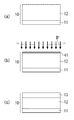
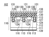
図20は、従来技術のトランジスタ102の断面図を示している。
このトランジスタ102は、トレンチ型パワーMOSFETであり、N+型不純物がシリコン単結晶中に高濃度にドープされた半導体基板111と、該半導体基板111上にエピタキシャル成長法によって形成されたN-型のシリコンエピタキシャル層から成るドレイン層112とを有している。
【0003】
符号110は、半導体基板111とドレイン層112とを有する処理基板を示しており、この処理基板110に半導体製造プロセスが施された結果、ドレイン層112内部の表面側に、P型のボディ層113が形成されており、該ボディ層113内部の表面近傍に、P+型のオーミック領域116と、N+型のソース領域130とが複数形成されている。
【0004】
ソース領域130の間の位置では、処理基板110表面が帯状にエッチングされ、細溝120が形成されている。
【0005】
細溝120の内周面には、ゲート絶縁膜124が形成されており、その細溝120の内部には、そのゲート絶縁膜124によって処理基板110とは非接触の状態で、ポリシリコンが充填され、そのポリシリコンによってゲート電極プラグ127が形成されている。
【0006】
各細溝120内のゲート電極プラグ127は、金属薄膜から成る不図示のゲート電極膜によって互いに接続されている。
【0007】
ソース領域130とオーミック領域116の表面には、金属薄膜から成るソース電極膜137が形成されている。細溝120上には層間絶縁膜131が形成されており、この層間絶縁膜131により、ソース電極膜137とゲート電極プラグ127とは電気的に絶縁されている。
【0008】
処理基板110の裏面、即ち、半導体基板111の表面にはドレイン電極膜139が形成されている。
【0009】
ソース電極膜137を接地電位に接続し、ドレイン電極膜139に正電圧を印加した状態で、ゲート電極膜に閾電圧以上の正電圧を印加すると、ゲート絶縁膜124とボディ層113の界面にN型の反転層が形成され、その反転層によって、ソース領域130とドレイン層112とが接続され、反転層を通って、ドレイン層112からソース領域130に向けて電流が流れる。この状態は、トランジスタ102が導通した状態であり、細溝120を用いないパワーMOSFETに存在するJFET領域が存在しないため、通常のパワーMOSFETに比べて導通抵抗が小さくなっている。
【0010】
そして、導通した状態からゲート電極膜の電位がソース電極膜137と同じ電位に変わると、反転層は消滅し、電流は流れなくなる。
【0011】
この状態では、ボディ層113とドレイン層112との間のPN接合は逆バイアスされており、そのPN接合のアバランシェ耐圧がトランジスタ102の耐圧と等しくなっている。
【0012】
一般に、PN接合のアバランシェ耐圧は、逆バイアスされたときの空乏層の形状によって異なるが、上記のようなトランジスタ102では、ドレイン層112内に広がる空乏層内の電界強度が不均一であるため、電界強度が強くなる部分でアバランシェ耐圧が決定され、耐圧が低くなってしまっている。
【0013】
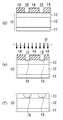
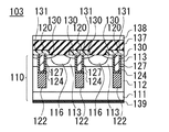
そこで図21のような構造の半導体装置103が提案されており、細溝120の下側にドレイン層112とは異なる導電型の埋込層122を形成し、ドレイン層112内に広がる空乏層の電界強度を緩和する試みが成されている。
【0014】
埋込層122は、一旦細溝120を深く掘削し、細溝120の内部の底部と側壁に充填物を成長させることで形成しており、充填物としては半導体単結晶や半導体多結晶を用いることができる。
【0015】
しかしながら、充填物としてシリコン単結晶を選択し、細溝120内にシリコンエピタキシャル層を成長させ、そのエピタキシャル層によって埋込層122を構成させた場合には、期待通りの耐圧が得られないという不都合が生じている。
【0016】
【発明が解決しようとする課題】
本発明は上記従来技術の不都合を解決するために創作されたものであり、その目的は、低抵抗高耐圧の半導体装置を提供することにある。
【0017】
【課題を解決するための手段】
本発明は、耐圧低下の原因が、細溝内にシリコンが均一にエピタキシャル成長せず、ボイドが生じてしまうことにあることを見出し、本発明を創作するに到ったものである。
【0018】
そして、請求項1記載の発明は、第1導電型のドレイン層と、前記ドレイン層と接して配置された第2導電型のボディ層と、前記ボディ層内に配置され、前記ドレイン層とは離間した第1導電型のソース領域と、前記ボディ層と前記ドレイン層とに亘って形成され、底面が前記ドレイン層内に位置する有底の細溝の前記ボディ層内に形成された前記細溝の内周面に形成されたゲート絶縁膜と、前記細溝内の前記ゲート絶縁膜と接触して配置されたゲート電極プラグとを有し、前記ゲート電極プラグに印加された電圧により、前記ゲート絶縁膜と前記ボディ層との間の界面に反転層が形成され、前記ソース領域と前記ドレイン層とが前記反転層によって接続されるトランジスタを製造する製造方法であって、底面と四側面に{1 0 0}面が露出する複数の直方体の前記細溝に、エピタキシャル成長によって、第2導電型のシリコン単結晶を成長させ、前記ドレイン層内に前記シリコン単結晶から成り、上端部が前記ボディ層と前記ドレイン層の境界よりも低い充填物を形成するトランジスタ充填物形成工程を有し、前記トランジスタ充填物形成工程では、前記充填物間の距離と、前記充填物の幅と、前記充填物の濃度と、前記ドレイン層の濃度とを、前記ドレイン層と前記ソース領域との間に、前記充填物が完全に空乏化する電圧が印加されたときには、前記充填物間に位置する部分の前記ドレイン層が完全に空乏化するように設定するトランジスタの製造方法である。
請求項2記載の発明は、前記充填物は、浮遊電位に置く請求項1記載のトランジスタの製造方法である。
請求項3記載の発明は、前記充填物は、前記ソース領域に電気的に接続する請求項1記載のトランジスタの製造方法である。
請求項4記載の発明は、前記ドレイン層のうち、前記ボディ層が位置する面とは反対側の面には第1導電型の半導体基板を有し、前記半導体基板表面には、該半導体基板とオーミック接続されたドレイン電極を設ける請求項1乃至請求項3のいずれか1項記載のトランジスタの製造方法である。
請求項5記載の発明は、前記ドレイン層のうち、前記ボディ層が位置する面とは反対側の面には第2導電型のコレクタ層を設け、前記コレクタ層表面には、該コレクタ層とオーミック接続されたコレクタ電極を設ける請求項1乃至請求項3のいずれか1項記載のトランジスタの製造方法である。
請求項6記載の発明は、前記ドレイン層のうち、前記ボディ層が位置する面とは反対側の面に、該ドレイン層とショットキー接合を形成するショットキー電極を設ける請求項1乃至請求項3のいずれか1項記載のトランジスタの製造方法である。
請求項7記載の発明は、第1導電型の主半導体層に形成され、底面と四側面に{1 0 0}面が露出する直方体の細溝に、エピタキシャル成長によって第2導電型の不純物が添加された充填物を形成するダイオード充填物形成工程と、前記主半導体層の表面と前記充填物の表面の両方に接触し、前記主半導体層とはショットキー接合を形成するショットキー電極を形成する電極形成工程と、を有し、前記ダイオード充填物形成工程では、前記ショットキー接合と、前記充填物と前記主半導体層との間のPN接合とに逆バイアスされる電圧が印加され、前記充填物の内部が完全に空乏化するときに、前記主半導体層の内部の空乏層の端部のうち、前記充填物と前記主半導体層とが形成するPN接合から横方向に広がった部分同士が接触するように、充填物の幅及び間隔と、濃度と、前記主半導体層の濃度とを設定するダイオードの製造方法である。
請求項8記載の発明は、前記ショットキー電極は、前記充填物とはオーミック接続させる請求項7記載のダイオードの製造方法である。
【0019】
【発明の実施の形態】
以下で図面を参照し、本発明の実施形態について説明する。
まず、図1(a)を参照し、符号10は、下記製造工程を適用する処理基板であり、シリコン単結晶から成る半導体基板11と、該半導体基板11表面にシリコンがエピタキシャル成長されて成るドレイン層12とを有している。本実施例では、第1導電型をN型、第2導電型をP型として説明する。
【0020】
半導体基板11は、N+型であり、抵抗率は0.003Ω・cm程度である。ドレイン層12はN-型で高抵抗である。ドレイン層12の厚みは18.2μm程度である。
【0021】
次に、図1(b)に示すように、ドレイン層12の表面にボロンイオン(B+)を照射するとドレイン層12の内部にボロンイオンが注入され、ドレイン層12内部の表面近くにP型注入層41が形成される。この状態では、ドレイン層12は、P型注入層41とシリコン基板11とで挟まれた状態になる。
【0022】
次いで、熱処理をし、P型注入層41中のボロンをドレイン層12内に拡散させると、図1(c)に示すように、ドレイン層12内部の表面側に、P型のボディ層13が形成される。ボディ層13は、最終的に底部がドレイン層12の表面から1.2μmの深さに位置するように設計されておりここでは、後述する熱処理よって拡散する分も考慮し、1.2μmよりも浅く拡散されている。
【0023】
そして、この状態では、ドレイン層12は処理基板10内に埋め込まれた状態になっており、処理基板10の表面にはドレイン層12は露出していない。
【0024】
次いで、図2(d)に示すように、ボディ層13の表面に、複数の細長の開口15が、所定間隔で互いに平行に形成されたレジスト膜14を形成する。
【0025】
次いで、レジスト膜14が形成された面に、P型の不純物(ここではボロンイオン:B+)を照射すると、レジスト膜14がマスクとなり、開口15の底面に露出するボディ層13表面にP型の不純物が注入され、図2(e)に示すように、ボディ層13内部の表面近傍に、開口15のパターンに従ったパターンで、P+型注入層19が形成される。
【0026】
レジスト膜14を除去した後、熱処理し、P+型注入層19中のボロン不純物を拡散させると、図2(f)に示すように、ボディ層13内部の表面近傍に、P+型のオーミック領域16が互いに平行に複数本形成される。ここではオーミック領域16の拡散深さは1.0μm程度である。
【0027】
次いで、図3(g)に示すように、ボディ層13とオーミック領域16とが露出した状態で、その表面にCVD法によってシリコン酸化膜17を形成した後、図3(h)に示すように、該シリコン酸化膜17表面にパターニングしたレジスト膜18を形成する。
【0028】
このレジスト膜18は、オーミック領域16の長手方向に沿い、オーミック領域16の間に位置する細長の開口42を有している。
【0029】
その状態で、エッチングし、開口42底面に位置するシリコン酸化膜17を除去すると、シリコン酸化膜17がレジスト膜18と同じ形状にパターニングされる。パターニングにより、シリコン酸化膜17には、図3(i)に示すように、レジスト膜18の開口42と同じ形状の開口43が形成される。
【0030】
この状態では、シリコン酸化膜17の開口43の底面には、処理基板10のうちのボディ層13の部分が露出されており、レジスト膜18を除去し、パターニングされたシリコン酸化膜17をマスクとし、開口43の底面に位置する部分の処理基板10をエッチングし、図4(j)に示すように、処理基板10に、シリコン酸化膜17の開口43と同じパターンの細溝20を形成する。
【0031】
この細溝20はボディ層13を貫通しており、細溝20の底面は、ボディ層13の下層に位置するドレイン層12の内部に達している。ここでは細溝20の処理基板10表面からの深さは12μmになっている。
【0032】
細溝20の開口部分の側面には、シリコン酸化膜17が露出しており、それよりも下方の部分では、処理基板10を構成するシリコンが露出している。
【0033】
レジスト膜18の開口42の幅は、オーミック領域16の間隔よりも狭く、且つ、開口42はオーミック領域16間の略中央に配置されている。従って、細溝20もオーミック領域16の間の位置であって、オーミック領域16の端部とは離間した位置に形成されているため、細溝20の側面には、処理基板10中のオーミック領域16は露出しておらず、ボディ層13と、その下層のドレイン層12とが露出している。細溝20の底面には、ドレイン層12が露出している。
【0034】
細溝20は上記のように形成されており、処理基板10の表面側では、細溝20の底面及び内周面にだけ処理基板10が露出している。
【0035】
この状態でCVD装置内に処理基板10を搬入し、高温に加熱してシリコンの原料ガスとP型の不純物を含有する添加ガスとを導入すると、細溝20の底面と内周面にシリコンと添加ガス中のP型の不純物とが析出し、P型のシリコン単結晶のエピタキシャル成長が開始される。
【0036】
ここで、処理基板10は、その表面の面方位が{1 0 0}であるものが用いられている。また、レジスト膜18の開口42の平面形状は長方形であり、開口42を形成する際に、処理基板10とレジスト膜18をパターニングするマスクとを相対的に位置合わせし、開口42の長辺又は短辺が、それぞれ処理基板10の{1 0 0}面を決めるx軸又はy軸の方向に沿うように配置されている。
【0037】
細溝20の開口の形状は開口42の平面形状と同じ形状であり、位置も同じであるから、細溝20の長辺又は短辺がx軸又はy軸の方向に沿っている。
【0038】
図11は、同一形状の複数の細溝20が互いに等間隔で平行に配置された状態を示す平面図であり、この図11では、細溝20の長辺a1、a2がx軸の方向に沿い、x軸と平行になっている。従って、細溝20の短辺b1、b2はy軸と平行になっている。
【0039】
また、図12は、細溝20の内部を表す斜視図である。この図12に示されているように、細溝20の内部空間、即ち、細溝20の内容積を構成する領域は直方体によって構成されている。即ち、細溝20の四側面A1、A2、B1、B2は、処理基板10の表面に対して垂直な平面であり、従って、隣り合う二側面は互いに直交している。また、細溝20の底面Cは、処理基板10の表面と平行であるから、四側面A1、A2、B1、B2に対して垂直になっている。
【0040】
従って細溝20の四側面A1、A2、B1、B2と底面Cの処理基板10表面が露出する部分は、シリコン単結晶の{1 0 0}面になっている。
{1 0 0}は、下記面方位、
【0041】
【数1】
![]()
の全てを表す。
【0043】
従って、処理基板10の表面の面方位が(1 0 0)であり、細溝20の長手方向の二側面A1、A2に(0 1 0)面が露出している場合、短辺方向の側面B1、B2には、(0 0 1)面又は、
【0044】
【数2】
が露出する(底面Cは、処理基板10の表面と同じ面方位である。)。
【0046】
従って、四側面A1、A2、B1、B2と底面Cに露出する処理基板10の面は全て同じ面方位{1 0 0}になるから、細溝20内には、処理基板10の各面からシリコンが均等にエピタキシャル成長し、図4(k)に示すように、細溝20のシリコン酸化膜17よりも下方の部分が、シリコンのエピタキシャル成長層から成る充填物22によって充填される。シリコン酸化膜17が露出する部分では、シリコンはエピタキシャル成長しないため、シリコン酸化膜17の開口43は残っている。
【0047】
ところで、細溝20内に{1 1 0}面や{1 1 1}が露出していた場合には、四側面A1、A2、B1、B2と底面Cに露出する処理基板10の表面が全てが同じ面方位になることはできないから、細溝20内に露出する処理基板10表面に、エピタキシャル成長速度が異なる部分が生じ、不均等にエピタキシャル成長したシリコンにより、細溝20内にボイドが形成されてしまう。
【0048】
図13は、本発明方法によって細溝20内をシリコンエピタキシャル成長層で充填した場合の、細溝20の断面電子顕微鏡写真である。この図13から分かるように、ボイドは生じていない。
【0049】
図14は、細溝の一側面A1に、(1 1 0)面を露出させ、シリコンエピタキシャル成長層によって充填した場合の細溝の断面電子顕微鏡写真である。この図14では、紙面縦方向に長いボイドが観察される。
【0050】
次いで、シリコン酸化膜17をマスクとし充填物22の上部をエッチングし、図4(l)に示すように、細溝20内部に、ボディ層13の上端から下端までと、ドレイン層12の上端から所定深さまでを露出させる。この状態では、充填物22の表面は、ボディ層13とドレイン層12が形成するPN接合よりも下方に位置している。ここでは、充填物22の表面は、処理基板10の表面から1.6μmの深さに位置している。
【0051】
次いで、この状態の処理基板10を熱酸化すると、図5(m)に示すように、細溝20内に露出する処理基板10表面に、シリコン酸化物薄膜から成るゲート絶縁膜24が形成される。
【0052】
この状態では、細溝20の底面Cには、ゲート絶縁膜24が配置されており、四側面A1、A2、B1、B2には、シリコン酸化膜17とゲート絶縁膜24とが配置されている。
【0053】
次いで、処理基板10の、細溝20の開口が位置する側の面にポリシリコンを堆積させ、図5(n)に示すように、ポリシリコン薄膜26を形成すると、細溝20内は、ポリシリコン薄膜26によって充填される。
【0054】
この状態では、ポリシリコン薄膜26は、細溝20内の他、シリコン酸化膜17の表面にも形成されており、その状態から、ポリシリコン薄膜26を所定量エッチングし、シリコン酸化膜17上に位置するポリシリコン薄膜26と、細溝20内部の上端部分のポリシリコン薄膜26を除去すると、各細溝20内のポリシリコン薄膜26は互いに分離され、図5(o)に示すように、細溝20の内部が、ポリシリコン薄膜26の残存部分から成るゲート電極プラグによってそれぞれ充填される。このゲート電極プラグ27は、細溝20内のゲート絶縁膜24で囲まれている。
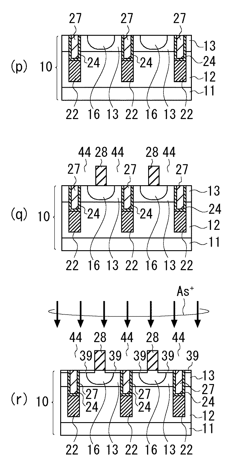
【0055】
次いで、図6(p)に示すように、シリコン酸化膜17を除去すると、処理基板10のボディ層13とオーミック領域16とが露出される。この状態では、細溝20内のゲート電極プラグ27の表面や、ゲート絶縁膜24の上端部も露出しており、ボディ層13の表面と、オーミック領域16の表面と、ゲート電極プラグ27の上端部と、ゲート絶縁膜24の上端部とで構成される処理基板10の表面は平坦になっている。
【0056】
オーミック領域16の平面形状と、細溝20の開口部分の形状、即ちゲート電極プラグ27の平面形状とは細長の長方形であり、互いに平行に交互に配置されている。
【0057】
次いで、図6(q)に示すように、オーミック領域16の幅方向中央位置に、オーミック領域16の幅よりも狭く、細長にパターニングされたレジスト膜28を形成する。このレジスト膜28の両側には、オーミック領域16が露出している。
【0058】
符号44はレジスト膜28が配置されていない露出面を示している。この状態で、図6(r)に示すように、レジスト膜28が形成された面にN型の不純物(ここでは砒素イオン:As+)を照射すると、露出面44内にN型不純物が注入され、オーミック領域16とボディ層13内部の表面近傍にN+型注入層39が形成される。このN+型注入層39は、レジスト膜28と細溝20との間に亘って形成されており、レジスト膜28で覆われていない部分のオーミック領域16とボディ層13の表面部分にN+型注入層39が形成されている。
【0059】
レジスト膜28を除去した後、熱処理を行うと、N+型注入層39中の不純物が拡散され、図7(s)に示すように、ボディ層13とオーミック領域16の表面近傍部分にN型のソース領域30が形成される。
【0060】
このソース領域30は、少なくとも細溝20の長手方向に沿った方向に伸びており、従って、少なくとも細溝20の長手方向の両側にはソース領域30の表面が露出されている。
【0061】
N+型注入層39中の不純物は横方向拡散し、オーミック領域16の表面を侵食するが、横方向拡散の量は少ないため、レジスト膜28が位置していた部分の幅方向中央の表面にはオーミック領域16が残り、その表面が露出している。
【0062】
また、N+型注入層39は、細溝20の側面に形成されたゲート絶縁膜24に接しており、N型の不純物はゲート絶縁膜24の内部には拡散しないため、ソース領域30は、ゲート絶縁膜24の上端部からソース領域30の拡散深さの分だけ、ゲート絶縁膜24と接触している。従って、この状態では、ソース領域30の底面とドレイン層12の上端部との間のゲート絶縁膜24は、ボディ層13と接触しており、その部分のゲート絶縁膜24とボディ層13の界面が所謂チャネル領域になる。
【0063】
次に、図7(t)に示すように、CVD法により、処理基板10全面にシリコン酸化膜から成る層間絶縁膜31を全面成膜し、図7(u)に示すように、該層間絶縁膜31の表面にパターニングしたレジスト膜32を形成する。
【0064】
このレジスト膜32には、パターニングによって細溝20の間の位置に細長の開口35が形成されており、レジスト膜32は、少なくとも細溝20の上部に配置されている。
【0065】
開口35の底面には層間絶縁膜31が露出しており、エッチングを行うと、図8(v)に示すように、層間絶縁膜31の開口35の底面の部分が除去され、層間絶縁膜31に、レジスト膜32の開口35と同じ平面パターンの開口36が形成される。
【0066】
層間絶縁膜31の開口35の底面には、幅方向の中央にオーミック領域16が露出しており、その両側位置にソース領域30が露出している。開口35の底面には、ゲート電極プラグ27の上端は露出していない。
【0067】
次に、レジスト膜32を除去した後、処理基板10の開口36を有する側の面に、蒸着法やスパッタリング法によってアルミニウム薄膜を形成し、パターニングし、ソース電極膜とゲート電極膜を形成する。ゲート電極膜とソース電極膜は、互いに分離されており、異なる電圧が印加できるようになっている。図8(w)の符号37はソース電極膜を示している。
【0068】
ソース電極膜37は、開口36底面において、ソース領域30とオーミック領域16とに接続されている。ソース電極膜37は、層間絶縁膜31によってゲート電極プラグ27から絶縁されている。
【0069】
他方、ゲート電極膜は、各細溝20内のゲート電極プラグ27に接続されており、各細溝20内のゲート電極プラグ27には、ゲート電極膜に印加された電圧が印加されるようになっている。
【0070】
次に、図8(x)に示すように、ソース電極膜37やゲート電極膜の表面にシリコン酸化物薄膜等から成る絶縁性保護膜38を形成し、パターニングしてソース電極膜37とゲート電極膜の一部を露出させた後、処理基板10の裏面に金属薄膜を形成し、その金属薄膜でドレイン電極膜25を構成させ、パワーMOSFET型のトランジスタ2を得る。このドレイン電極膜25は、半導体基板11とオーミック接合を形成している。
【0071】
このようなトランジスタ2では、1枚の処理基板10中に複数個形成されており、ダイシング工程により、トランジスタ2を1個ずつ切り離した後、ゲート電極膜、ソース電極膜37、及びドレイン電極膜25を金属端子に接続し、樹脂封止するとパッケージ化されたトランジスタ2が得られる。
【0072】
金属端子を電源や電気回路に接続することにより、ソース電極膜37を接地電位に接続し、ドレイン電極膜25に正電圧を印加した状態で、ゲート電極膜に電圧を印加し、各細溝20内のゲート電極プラグ27に閾電圧以上の大きさの正電圧を印加すると、チャネル領域(ボディ層13とゲート絶縁膜24の界面)にN型の反転層が形成され、ソース領域30とドレイン層12とが反転層によって接続され、ドレイン層12からソース領域30に向けて電流が流れる。この状態では、トランジスタ2は導通状態にある。
【0073】
その状態から、各ゲート電極プラグ27をソース電位と同じ電位にすると、反転層は消滅し、電流は流れなくなる。この状態ではトランジスタ2は遮断状態にある。
【0074】
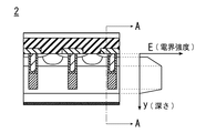
トランジスタ2が遮断状態にあり、ドレイン電極膜25とソース電極膜37の間に大きな電圧が印加された状態では、ボディ層13とドレイン層12とで構成されるPN接合が逆バイアスされ、ボディ層13内とドレイン層12内に空乏層が広がる。
【0075】
細溝20の底部に半導体エピタキシャル成長物から成る充填物22が配置されており、その充填物22の導電型はドレイン層12の導電型とは逆になっている。充填物22は、ドレイン層12とは電気的に接続されていないから、ボディ層13内に空乏層が広がるときには充填物22内にも空乏層が広がるようになっている。
【0076】
図9の符号48は、P型のボディ層13と充填物22と、N型のドレイン層12との間に形成されるPN接合から、ドレイン層12内に広がる空乏層の端部を示しており、符号49は、充填物22とドレイン層12との間に形成されるPN接合から充填物22内に広がった空乏層の端部を示している。
【0077】
この図9の状態から、ドレイン電極膜25とソース電極膜37の間の電圧が更に大きくなると、充填物22は完全に空乏化する。
【0078】
本発明のトランジスタ2では、充填物22間の距離及び充填物22の幅と、充填物22の濃度及びドレイン層12の濃度とが、最適値に設定されることで、ドレイン電極膜25とソース電極膜37の間に、充填物22が完全に空乏化する電圧が印加されたときには、細溝20及び充填物22間に位置する部分のドレイン層12も完全に空乏化するようになっている。
【0079】
ドレイン層12の、充填物22間に位置する部分が完全に空乏化した状態では、ドレイン層12内に広がった空乏層の内部の電界強度は深さ方向で一定値になっている。
【0080】
この状態のトランジスタ2の内部の位置と電界強度の関係を図10のグラフに示す。この図10のグラフは、細溝20の間の位置であって、ソース領域30と、ボディ層13と、ドレイン層12とを通るA−A線に沿った方向の電界強度である。
【0081】
この場合、充填物22内にボイドが存在すると、その部分で耐圧が低下するが、本発明のトランジスタ2では、{1 0 0}面から等速度でエピタキシャル成長した半導体結晶によって充填物22が構成されており、ボイドが存在しないため耐圧の低下が生じない。
【0082】
以上は、電界効果MOSトランジスタ型の実施例について説明したが、本発明はそれに限定されるものではない。
【0083】
図15の符号3は、本発明の他の例であるPN接合型のIGBTを示している。この図15では、図8(x)に示したトランジスタ2と同じ部材には同じ符号を付してある。このトランジスタ3(及び後述する図16のトランジスタ4)の細溝20の側面及び底面は、{1 0 0}面であり、細溝20内に充填された充填物22は、{1 0 0}面からエピタキシャル成長した半導体単結晶であり、平面パターンは図11のように、複数の細溝20が平行に配置されており、各細溝20の内容積は、図12に示したように、直方体によって構成されている。
【0084】
図15のトランジスタ3が図8(x)のトランジスタ2と異なる部分は、図8(x)のトランジスタ2の処理基板10は、エピタキシャル成長法により、N型(第1の導電型)のドレイン層12がN型の半導体単結晶である半導体基板11上に形成されていたが、図15のトランジスタ3のN型(第1の導電型)の処理基板71では、N型のドレイン層12は、エピタキシャル成長法により、P型の半導体基板45上に形成されている。
【0085】
図15の符号46は、P型の半導体基板45表面に形成された金属薄膜から成るコレクタ電極を示しており、このコレクタ電極46は、P型の半導体基板45とオーミック接合を形成している。
【0086】
このようなトランジスタ3では、半導体基板45からドレイン層12内に少数キャリアが注入され、ドレイン層12の伝導度が変調する結果、導通状態におけるドレイン層12の抵抗値は、MOSFET型のトランジスタ2よりも小さくなる。
【0087】
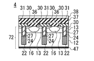
次に、図16のトランジスタ4を説明する。このトランジスタ4は、本発明の一例のショットキー接合型のIGBTであり、図15のトランジスタ3の場合と同様に、図8(x)と同じ部材には同じ符号を付して説明を省略する。
【0088】
図16のトランジスタ4の処理基板72は、高抵抗のN型(第1の導電型)ドレイン層12の表面に、金属薄膜から成るショットキー電極47が形成されている。
【0089】
このショットキー電極47は、ドレイン層12とショットキー接合を形成しており、ショットキー電極47とドレイン層12との間には、ショットキー電極47がアノード電極となり、ドレイン層12がカソード電極となるダイオードが形成されている。
【0090】
このようなトランジスタ4では、ショットキー電極47からドレイン層12内に少数キャリアが注入され、ドレイン層12の伝導度変調が生じ、動作状態におけるドレイン層12の抵抗値が小さくなる。但し、その抵抗値は、図15に示したPN接合型のIGBTよりも大きい。
【0091】
上記各トランジスタ2〜4では、細溝20内の充填物22はソース電極膜37やゲート電極プラグ27やドレイン電極膜25、コレクタ電極46又はショットキー電極47には接続されておらず、浮遊電位に置かれていたが、各細溝20内の充填物22をソース電極膜37に接続し、充填物22にソース領域30と同じ電圧が印加されるようにしてもよい。
【0092】
但し、充填物22を浮遊電位に置いたときとソース電極膜37に接続したときとは、空乏層の拡がり方が少し異なる。
【0093】
充填物22を浮遊電位に置いたときには、ボディ層13とドレイン層12の界面のPN接合からドレイン層12内に広がった空乏層の端部が充填物22に達したときに、充填物22のうちの空乏層の端部と接する部分は、ドレイン電極膜25の電位と同じ電位になる。
【0094】
そして、ドレイン電極膜25とソース電極膜37の間の電位差がそれ以上大きくなると、空乏層は充填物22の内部にも生じるようになる。
【0095】
それに対し、充填物22をソース電極膜37に接続した場合には、充填物22はソース電極膜37と同じ電位であり、ドレイン電極膜25とソース電極膜37の間に電圧が印加され、充填物22とドレイン層12との間のPN接合が逆バイアスされると、空乏層は充填物22の内部に直ちに発生する。
【0096】
いずれにしろ、充填物22内が完全に空乏化すると共に、充填物22間に位置する部分のドレイン層12が空乏化するとき、ボディ層13とドレイン層12との界面のPN接合から充填物22の底面までの電界強度Eは、図10に示すように一定になる。
【0097】
このため、従来のように集中的に強度の強い電界が加わらず、従来構造のトランジスタと同じ電圧を印加した場合には、ボディ層13とドレイン層12との界面から充填物22の底面までには、従来構造のトランジスタよりも小さい電界が加わるので、従来よりも耐圧が高くなる。
【0098】
以上は、実施例としてトランジスタ2〜4を説明したが、本発明はトランジスタに限定されるものではなく、ダイオードも含まれる。
【0099】
図18(f)の符号5は、本発明の一例のダイオードを示している。このダイオード5の製造工程を説明すると、先ず、図17(a)に示すように、N+型の半導体基板51と、該半導体基板51上に配置されたN-型の主半導体層52とを有する処理基板50を用意し、主半導体層52表面に細長の細溝53を形成する。
【0100】
この細溝53の配置状態も、図11に示した細溝20と同様に、複数の細溝53が互いに平行に配置されており、各細溝53の内容積は、図12の細溝20と同様に、直方体によって構成されている。
【0101】
半導体基板51はN型の不純物が高濃度にドープされたシリコン等の半導体単結晶から成り、主半導体層52はN型の不純物が少量ドープされ、エピタキシャル成長法によって形成された半導体単結晶によって構成されている。
【0102】
細溝53の開口の形状は長方形であり、細溝53の四側面は主半導体層52の表面に対して垂直になっている。また、細溝53の底面は、主半導体層52の表面と平行になっている。
【0103】
細溝53の側面及び底面は、{1 0 0}面であり、処理基板50の細溝53が形成された面にシリコンがエピタキシャル成長すると、図17(c)に示すように、細溝53内は、シリコンエピタキシャル層55によって充填される。エピタキシャル成長の際にはP型の不純物が添加され、シリコンエピタキシャル層55はP型になっている。
【0104】
この状態では、細溝53間に露出する主半導体層52の表面にも、シリコンエピタキシャル層55は成長しており、図18(d)に示すように、主半導体層52表面が露出するまでシリコンエピタキシャル層55をエッチングすると、各細溝53内部に、シリコンエピタキシャル層55の残部によって構成された充填物57が形成される。主半導体層52表面が露出した状態では、各細溝53内の充填物57は、互いに分離されている。
【0105】
次に、処理基板50の充填物57及び主半導体層52が露出する側の表面に金属薄膜を形成し、不要部分をエッチング除去し、その金属薄膜の残部で第1の電極59を形成する。
【0106】
この第1の電極59は、主半導体層52とはショットキー接合を形成し、充填物57とはオーミック接合を形成している。充填物57の導電型と主半導体層52の導電型とは互いに反対になっており、主半導体層52と充填物57との間にはPN接合が形成されている。
【0107】
次に、図18(f)に示すように、半導体基板51の表面に、半導体基板51とオーミック接合する金属膜を形成し、その金属膜によって第2の電極60を構成させる。
【0108】
このダイオード5では、第2の電極60に負電圧、第1の電極59に正電圧を印加すると、第1の電極59と主半導体層52との間のショットキー接合が順バイアスされ、第1の電極59から第2の電極60に向けて電流が流れる。
【0109】
このとき、充填物57と主半導体層52との間のPN接合も順バイアスされるが、PN接合の障壁高さはショットキー接合の障壁高さよりも高いので、PN接合には電流は流れないか、流れても僅かである。
【0110】
それとは逆に、第2の電極60に正電圧、第1の電極59に負電圧を印加すると、第1の電極59と主半導体層52との間のショットキー接合と、充填物57と主半導体層52との間のPN接合が逆バイアスされ、電流は流れなくなる。
【0111】
このとき、ショットキー接合とPN接合の両方から主半導体層52内に空乏層が広がる。図19の符号61は、ショットキー接合面及びPN接合面から主半導体層52内に広がる空乏層の端部を示しており、同図の符号62は、PN接合面から充填物57内に広がる空乏層の端部を示している。
【0112】
このダイオード5では、充填物57の幅及び間隔と、その濃度と、主半導体層52の濃度とが最適値に設定されることで、充填物57の内部が完全に空乏化するときに、主半導体層52内部の空乏層の端部の、PN接合から横方向に広がった部分同士が接触するようになっている。
【0113】
このように、本発明のダイオード5でも、主半導体層52内に広がった空乏層の内部の電界強度は、深さ方向で一定値になっている。
【0114】
以上は、トランジスタとダイオードに属する本発明の実施例について説明したが、本発明の半導体装置は、溝内が半導体のエピタキシャル成長物で充填された半導体装置に広く用いることが可能である。
【0115】
なお、以上の例では、N型が第1導電型であり、P型が第2導電型であったが、N型とP型をそっくり入れ替え、P型を第1導電型とし、N型を第2導電型としたトランジスタ又はダイオードも本発明に含まれることは言うまでもない。
【0116】
【発明の効果】
導通抵抗が小さく、高耐圧のトランジスタとダイオードが得られる。
【図面の簡単な説明】
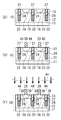
【図1】(a)〜(c):本発明の一実例のトランジスタの製造工程を説明するための図(1)
【図2】(d)〜(f):本発明の一実例のトランジスタの製造工程を説明するための図(2)
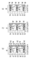
【図3】(g)〜(i):本発明の一実例のトランジスタの製造工程を説明するための図(3)
【図4】(j)〜(l):本発明の一実例のトランジスタの製造工程を説明するための図(4)
【図5】(m)〜(o):本発明の一実例のトランジスタの製造工程を説明するための図(5)
【図6】(p)〜(r):本発明の一実例のトランジスタの製造工程を説明するための図(6)
【図7】(s)〜(u):本発明の一実例のトランジスタの製造工程を説明するための図(7)
【図8】(v)〜(x):本発明の一実例のトランジスタの製造工程を説明するための図(8)
【図9】本発明のトランジスタ内部の空乏層の状態を説明するための図
【図10】本発明のトランジスタ内部の電界強度の分布を説明するための図
【図11】本発明のトランジスタ及びダイオードの細溝の配置を説明するための平面図
【図12】本発明のトランジスタ及びダイオードの細溝の立体形状を説明するための斜視図
【図13】細溝の側面に{1 0 0}を露出させた本発明のトランジスタの充填物の断面顕微鏡写真
【図14】細溝の側面に{1 1 0}を露出させたトランジスタの充填物の断面顕微鏡写真
【図15】PN接合型IGBTである本発明のトランジスタの一例を示す図
【図16】ショットキー接合型IGBTである本発明のトランジスタの一例を示す図
【図17】(a)〜(c):本発明のダイオードの製造工程を説明するための図(1)
【図18】(d)〜(f):本発明のダイオードの製造工程を説明するための図(2)
【図19】本発明のダイオード内部の空乏層の状態を説明するための図
【図20】従来技術のトランジスタを説明するための図
【図21】充填物を有するトランジスタを説明するための図
【符号の説明】
2〜4……トランジスタ
5……ダイオード
11、45……半導体基板
12……ドレイン層
13……ボディ層
20、53……細溝
22、57……充填物
24……ゲート絶縁膜
27……ゲート電極プラグ
30……ソース領域
46……コレクタ電極
47……ショットキー電極[0001]
BACKGROUND OF THE INVENTION
The present invention relates to a transistor and a diode, and more particularly to a transistor and a diode having a structure in which a semiconductor crystal is epitaxially grown in a narrow groove.
[0002]
[Prior art]
FIG. 20 shows a cross-sectional view of a
This
[0003]
[0004]
At the position between the
[0005]
A
[0006]
The
[0007]
A
[0008]
A
[0009]
When a positive voltage higher than the threshold voltage is applied to the gate electrode film while the
[0010]
When the potential of the gate electrode film changes from the conductive state to the same potential as that of the
[0011]
In this state, the PN junction between the
[0012]
In general, the avalanche breakdown voltage of the PN junction varies depending on the shape of the depletion layer when reverse-biased, but in the
[0013]
Accordingly, a
[0014]
The buried
[0015]
However, when a silicon single crystal is selected as the filling material, a silicon epitaxial layer is grown in the
[0016]
[Problems to be solved by the invention]
The present invention was created to solve the above-described disadvantages of the prior art, and an object thereof is to provide a semiconductor device having a low resistance and a high breakdown voltage.
[0017]
[Means for Solving the Problems]
The present invention has found that the cause of the decrease in breakdown voltage is that silicon does not uniformly grow epitaxially in the narrow groove and voids are generated, and the present invention has been created.
[0018]
According to the first aspect of the present invention, there is provided a first conductivity type drain layer, a second conductivity type body layer disposed in contact with the drain layer, and the body layer. The thin film is formed in the body layer of a narrow groove having a bottom and is formed across the source region of the first conductivity type and the body layer and the drain layer which are separated from each other, and the bottom surface is located in the drain layer. A gate insulating film formed on the inner peripheral surface of the groove, and a gate electrode plug disposed in contact with the gate insulating film in the narrow groove, and a voltage applied to the gate electrode plug A manufacturing method for manufacturing a transistor in which an inversion layer is formed at an interface between a gate insulating film and the body layer, and the source region and the drain layer are connected to each other by the inversion layer . {1 0 0} face is dew A plurality of rectangular parallelepiped of the thin groove that, by epitaxial growth, to grow a silicon single crystal of the second conductivity type, wherein Ri formed from the silicon single crystal into the drain layer, the upper end portion of the drain layer and the body layer boundary A transistor filling step for forming a lower filling, wherein in the transistor filling forming step, the distance between the fillings, the width of the filling, the concentration of the filling, and the drain layer When a voltage is applied between the drain layer and the source region so that the filling is completely depleted, a portion of the drain layer located between the fillings is completely depleted. This is a method for manufacturing a transistor to be set as described above.
A second aspect of the present invention is the method of manufacturing a transistor according to the first aspect, wherein the filling is placed at a floating potential.
The invention according to
According to a fourth aspect of the present invention, the drain layer includes a first conductivity type semiconductor substrate on a surface opposite to a surface on which the body layer is located, and the semiconductor substrate surface includes the semiconductor substrate. 4. The method of manufacturing a transistor according to
According to a fifth aspect of the present invention, a second conductivity type collector layer is provided on a surface of the drain layer opposite to the surface on which the body layer is located, and the collector layer surface is provided with the collector layer. The transistor manufacturing method according to
According to a sixth aspect of the present invention, a Schottky electrode that forms a Schottky junction with the drain layer is provided on a surface of the drain layer opposite to the surface on which the body layer is located. 4. A method for producing a transistor according to any one of 3 above.
According to a seventh aspect of the invention, an impurity of the second conductivity type is added by epitaxial growth to a rectangular parallelepiped groove formed in the first conductivity type main semiconductor layer and exposing the {1 0 0} plane on the bottom surface and the four side surfaces. Forming a diode filling, and forming a Schottky electrode that contacts both the surface of the main semiconductor layer and the surface of the filling, and forms a Schottky junction with the main semiconductor layer. An electrode forming step, and in the diode filling step, a voltage reversely biased is applied to the Schottky junction and a PN junction between the filling and the main semiconductor layer, and the filling is performed. When the interior of the object is completely depleted, the portions of the end portion of the depletion layer inside the main semiconductor layer that are spread laterally from the PN junction formed by the filler and the main semiconductor layer are To touch , The width and spacing of the fill is a method for producing a diode to set the concentration and the concentration of the main semiconductor layer.
The invention according to claim 8 is the diode manufacturing method according to claim 7, wherein the Schottky electrode is in ohmic contact with the filler.
[0019]
DETAILED DESCRIPTION OF THE INVENTION
Embodiments of the present invention will be described below with reference to the drawings.
First, referring to FIG. 1A,
[0020]
The
[0021]
Next, as shown in FIG. 1B, when the surface of the
[0022]
Next, when heat treatment is performed and boron in the P-
[0023]
In this state, the
[0024]
Next, as shown in FIG. 2 (d), a resist
[0025]
Next, when the surface on which the resist
[0026]
When the resist
[0027]
Next, as shown in FIG. 3G, after the
[0028]
The resist
[0029]
In this state, etching is performed to remove the
[0030]
In this state, the
[0031]
The
[0032]
The
[0033]
The width of the
[0034]
The
[0035]
In this state, when the
[0036]
Here, the
[0037]
Since the shape of the opening of the
[0038]
FIG. 11 is a plan view showing a state in which a plurality of
[0039]
FIG. 12 is a perspective view showing the inside of the
[0040]
Accordingly, the four side surfaces A 1 , A 2 , B 1 , B 2 of the
{1 0 0} is the following plane orientation,
[0041]
[Expression 1]
![]()
Represents all of
[0043]
Therefore, when the surface orientation of the surface of the
[0044]
[Expression 2]
Are exposed (the bottom surface C has the same plane orientation as the surface of the processing substrate 10).
[0046]
Accordingly, the four side surfaces A 1 , A 2 , B 1 , B 2 and the surface of the
[0047]
By the way, when the {1 1 0} plane or {1 1 1} is exposed in the
[0048]
FIG. 13 is a cross-sectional electron micrograph of the
[0049]
FIG. 14 is a cross-sectional electron micrograph of the narrow groove when the (1 1 0) plane is exposed on one side face A 1 of the narrow groove and filled with the silicon epitaxial growth layer. In FIG. 14, a long void is observed in the vertical direction of the paper.
[0050]
Next, the upper portion of the filling 22 is etched using the
[0051]
Next, when the
[0052]
In this state, the
[0053]
Next, when polysilicon is deposited on the surface of the
[0054]
In this state, the polysilicon thin film 26 is formed not only in the
[0055]
Next, as shown in FIG. 6P, when the
[0056]
The planar shape of the
[0057]
Next, as shown in FIG. 6 (q), a resist
[0058]
[0059]
When the heat treatment is performed after removing the resist
[0060]
The
[0061]
Impurities in the N + -type implantation layer 39 diffuse in the lateral direction and erode the surface of the
[0062]
Further, since the N + type implantation layer 39 is in contact with the
[0063]
Next, as shown in FIG. 7 (t), an
[0064]
In the resist
[0065]
The
[0066]
On the bottom surface of the
[0067]
Next, after removing the resist
[0068]
The
[0069]
On the other hand, the gate electrode film is connected to the
[0070]
Next, as shown in FIG. 8 (x), an insulating
[0071]
In such a
[0072]
By connecting the metal terminal to a power source or an electric circuit, the
[0073]
In this state, when each
[0074]
When the
[0075]
A filling 22 made of a semiconductor epitaxial growth is disposed at the bottom of the
[0076]
[0077]
When the voltage between the
[0078]
In the
[0079]
In the state where the portion of the
[0080]
The relationship between the position inside the
[0081]
In this case, if a void is present in the filling 22, the breakdown voltage is reduced at that portion, but in the
[0082]
The field effect MOS transistor type embodiment has been described above, but the present invention is not limited thereto.
[0083]
[0084]
15 differs from the
[0085]
[0086]
In such a
[0087]
Next, the
[0088]
In the
[0089]
The
[0090]
In such a
[0091]
In each of the
[0092]
However, the way in which the depletion layer expands is slightly different between when the filling 22 is placed at a floating potential and when it is connected to the
[0093]
When the filling
[0094]
When the potential difference between the
[0095]
In contrast, when connecting the
[0096]
In any case, when the inside of the filling 22 is completely depleted and the portion of the
[0097]
For this reason, when an electric field having a strong intensity is not applied intensively as in the prior art and the same voltage as that of the transistor having the conventional structure is applied, the interface between the
[0098]
Although the
[0099]
[0100]
Similarly to the
[0101]
The
[0102]
The shape of the opening of the
[0103]
The side surface and the bottom surface of the
[0104]
In this state, the
[0105]
Next, a metal thin film is formed on the surface of the
[0106]
The
[0107]
Next, as illustrated in FIG. 18F, a metal film that is in ohmic contact with the
[0108]
In this
[0109]
At this time, the PN junction between the
[0110]
On the contrary, when a positive voltage is applied to the
[0111]
At this time, a depletion layer spreads in the
[0112]
In the
[0113]
Thus, also in the
[0114]
Although the embodiments of the present invention belonging to the transistor and the diode have been described above, the semiconductor device of the present invention can be widely used for semiconductor devices in which the trench is filled with a semiconductor epitaxial growth product.
[0115]
In the above example, the N-type is the first conductivity type and the P-type is the second conductivity type. However, the N-type and the P-type are completely interchanged, the P-type is the first conductivity type, and the N-type is It goes without saying that a transistor or a diode having the second conductivity type is also included in the present invention.
[0116]
【Effect of the invention】
Transistors and diodes with low conduction resistance and high breakdown voltage can be obtained.
[Brief description of the drawings]
FIGS. 1A to 1C are diagrams (1) for explaining a manufacturing process of a transistor according to an example of the present invention;
FIGS. 2D to 2F are diagrams (2) for explaining a manufacturing process of a transistor of an example of the present invention;
3 (g) to (i) are diagrams (3) for explaining a manufacturing process of a transistor according to an example of the present invention;
4 (j) to (l) are diagrams (4) for explaining a manufacturing process of a transistor according to an example of the present invention;
FIGS. 5A to 5O are diagrams (5) for explaining a manufacturing process of a transistor of an example of the present invention;
6 (p) to (r) are diagrams (6) for explaining a manufacturing process of a transistor according to an example of the present invention;
7 (s) to (u) are diagrams (7) for explaining a manufacturing process of the transistor of the example of the present invention;
8 (v) to (x) are diagrams (8) for explaining a manufacturing process of a transistor according to an example of the present invention;
FIG. 9 is a diagram for explaining a state of a depletion layer inside a transistor according to the present invention. FIG. 10 is a diagram for explaining a distribution of electric field strength inside the transistor according to the present invention. FIG. 12 is a perspective view for explaining the three-dimensional shape of the narrow grooves of the transistor and the diode of the present invention. FIG. 13 is a side view of the narrow groove with {1 0 0}. FIG. 14 is a cross-sectional photomicrograph of the exposed transistor filling of the present invention. FIG. 14 is a cross-sectional photomicrograph of the transistor filling with exposed {1 1 0} on the side of the narrow groove. FIG. 16 is a diagram showing an example of a transistor of the present invention which is a Schottky junction type IGBT. FIGS. 17A to 17C are diagrams illustrating a manufacturing process of a diode of the present invention. Do Because of Figure (1)
18 (d) to 18 (f) are diagrams (2) for explaining the manufacturing process of the diode of the present invention.
FIG. 19 is a diagram for explaining a state of a depletion layer inside a diode according to the present invention. FIG. 20 is a diagram for explaining a conventional transistor. FIG. 21 is a diagram for explaining a transistor having a filling. Explanation of symbols]
2 to 4...
Claims (8)
前記ドレイン層と接して配置された第2導電型のボディ層と、
前記ボディ層内に配置され、前記ドレイン層とは離間した第1導電型のソース領域と、
前記ボディ層と前記ドレイン層とに亘って形成され、底面が前記ドレイン層内に位置する有底の細溝の前記ボディ層内に形成された前記細溝の内周面に形成されたゲート絶縁膜と、
前記細溝内の前記ゲート絶縁膜と接触して配置されたゲート電極プラグとを有し、
前記ゲート電極プラグに印加された電圧により、前記ゲート絶縁膜と前記ボディ層との間の界面に反転層が形成され、前記ソース領域と前記ドレイン層とが前記反転層によって接続されるトランジスタを製造する製造方法であって、
底面と四側面に{1 0 0}面が露出する複数の直方体の前記細溝に、エピタキシャル成長によって、第2導電型のシリコン単結晶を成長させ、前記ドレイン層内に前記シリコン単結晶から成り、上端部が前記ボディ層と前記ドレイン層の境界よりも低い充填物を形成するトランジスタ充填物形成工程を有し、
前記トランジスタ充填物形成工程では、前記充填物間の距離と、前記充填物の幅と、前記充填物の濃度と、前記ドレイン層の濃度とを、前記ドレイン層と前記ソース領域との間に、前記充填物が完全に空乏化する電圧が印加されたときには、前記充填物間に位置する部分の前記ドレイン層が完全に空乏化するように設定するトランジスタの製造方法。A drain layer of a first conductivity type;
A body layer of a second conductivity type disposed in contact with the drain layer;
A source region of a first conductivity type disposed in the body layer and spaced apart from the drain layer;
Gate insulation formed on the inner peripheral surface of the narrow groove formed in the body layer of the bottomed narrow groove formed across the body layer and the drain layer and having a bottom surface located in the drain layer A membrane,
A gate electrode plug disposed in contact with the gate insulating film in the narrow groove ;
A transistor in which an inversion layer is formed at the interface between the gate insulating film and the body layer by the voltage applied to the gate electrode plug , and the source region and the drain layer are connected by the inversion layer is manufactured. A manufacturing method for
A plurality of rectangular parallelepiped of the fine grooves on the bottom and four sides {1 0 0} plane is exposed, by epitaxial growth, to grow a silicon single crystal of the second conductivity type, Ri formed from the silicon single crystal in the drain layer A transistor filling step of forming a filling whose upper end is lower than the boundary between the body layer and the drain layer ;
In the transistor filling step, the distance between the fillings, the width of the filling, the concentration of the filling, and the concentration of the drain layer are set between the drain layer and the source region. A method for manufacturing a transistor, wherein the drain layer in a portion located between the fillings is set to be completely depleted when a voltage at which the filling is completely depleted is applied.
前記半導体基板表面には、該半導体基板とオーミック接続されたドレイン電極を設ける請求項1乃至請求項3のいずれか1項記載のトランジスタの製造方法。Of the drain layer, a surface opposite to the surface on which the body layer is located has a first conductivity type semiconductor substrate,
4. The method of manufacturing a transistor according to claim 1, wherein a drain electrode that is ohmically connected to the semiconductor substrate is provided on the surface of the semiconductor substrate.
前記コレクタ層表面には、該コレクタ層とオーミック接続されたコレクタ電極を設ける請求項1乃至請求項3のいずれか1項記載のトランジスタの製造方法。A second conductivity type collector layer is provided on the surface of the drain layer opposite to the surface on which the body layer is located,
4. The method of manufacturing a transistor according to claim 1, wherein a collector electrode that is ohmically connected to the collector layer is provided on a surface of the collector layer.
前記主半導体層の表面と前記充填物の表面の両方に接触し、前記主半導体層とはショットキー接合を形成するショットキー電極を形成する電極形成工程と、を有し、
前記ダイオード充填物形成工程では、前記ショットキー接合と、前記充填物と前記主半導体層との間のPN接合とに逆バイアスされる電圧が印加され、前記充填物の内部が完全に空乏化するときに、前記主半導体層の内部の空乏層の端部のうち、前記充填物と前記主半導体層とが形成するPN接合から横方向に広がった部分同士が接触するように、充填物の幅及び間隔と、濃度と、前記主半導体層の濃度とを設定するダイオードの製造方法。A diode which is formed in a first conductive type main semiconductor layer and forms a filling in which a second conductive type impurity is added by epitaxial growth in a rectangular parallelepiped groove having a {1 0 0} plane exposed on the bottom surface and four side surfaces Filling formation process;
An electrode forming step of contacting a surface of the main semiconductor layer and a surface of the filler, and forming a Schottky electrode that forms a Schottky junction with the main semiconductor layer;
In the diode filling process, a reverse-biased voltage is applied to the Schottky junction and a PN junction between the filling and the main semiconductor layer, and the inside of the filling is completely depleted. Sometimes, the width of the filling is such that, of the end portion of the depletion layer inside the main semiconductor layer, the portions extending laterally from the PN junction formed by the filling and the main semiconductor layer are in contact with each other. And a method for manufacturing a diode, which sets a distance, a concentration, and a concentration of the main semiconductor layer.
Priority Applications (4)
| Application Number | Priority Date | Filing Date | Title |
|---|---|---|---|
| JP2001260869A JP4865166B2 (en) | 2001-08-30 | 2001-08-30 | Transistor manufacturing method, diode manufacturing method |
| US10/197,565 US7230298B2 (en) | 2001-08-30 | 2002-07-18 | Transistor having narrow trench filled with epitaxially-grown filling material free of voids |
| EP02016509A EP1289022A3 (en) | 2001-08-30 | 2002-07-23 | Power MOSFET transistor and Schottky diode |
| US11/785,808 US7855413B2 (en) | 2001-08-30 | 2007-04-20 | Diode with low resistance and high breakdown voltage |
Applications Claiming Priority (1)
| Application Number | Priority Date | Filing Date | Title |
|---|---|---|---|
| JP2001260869A JP4865166B2 (en) | 2001-08-30 | 2001-08-30 | Transistor manufacturing method, diode manufacturing method |
Related Child Applications (1)
| Application Number | Title | Priority Date | Filing Date |
|---|---|---|---|
| JP2011227832A Division JP2012069960A (en) | 2011-10-17 | 2011-10-17 | Epitaxial silicon growth method |
Publications (2)
| Publication Number | Publication Date |
|---|---|
| JP2003069017A JP2003069017A (en) | 2003-03-07 |
| JP4865166B2 true JP4865166B2 (en) | 2012-02-01 |
Family
ID=19088004
Family Applications (1)
| Application Number | Title | Priority Date | Filing Date |
|---|---|---|---|
| JP2001260869A Expired - Lifetime JP4865166B2 (en) | 2001-08-30 | 2001-08-30 | Transistor manufacturing method, diode manufacturing method |
Country Status (3)
| Country | Link |
|---|---|
| US (2) | US7230298B2 (en) |
| EP (1) | EP1289022A3 (en) |
| JP (1) | JP4865166B2 (en) |
Families Citing this family (29)
| Publication number | Priority date | Publication date | Assignee | Title |
|---|---|---|---|---|
| JP4865166B2 (en) * | 2001-08-30 | 2012-02-01 | 新電元工業株式会社 | Transistor manufacturing method, diode manufacturing method |
| EP2259325B1 (en) | 2002-02-20 | 2013-12-25 | Shindengen Electric Manufacturing Co., Ltd. | Transistor device |
| JP3914785B2 (en) | 2002-02-20 | 2007-05-16 | 新電元工業株式会社 | Diode element |
| US6841825B2 (en) | 2002-06-05 | 2005-01-11 | Shindengen Electric Manufacturing Co., Ltd. | Semiconductor device |
| JP3971670B2 (en) | 2002-06-28 | 2007-09-05 | 新電元工業株式会社 | Semiconductor device |
| AU2003268710A1 (en) | 2002-10-04 | 2004-04-23 | Shindengen Electric Manufacturing Co., Ltd. | Semiconductor device and process for fabricating the same |
| JP5299373B2 (en) * | 2003-01-16 | 2013-09-25 | 富士電機株式会社 | Semiconductor element |
| JP4133548B2 (en) * | 2003-04-25 | 2008-08-13 | 新電元工業株式会社 | Semiconductor device |
| JP3689419B1 (en) * | 2004-03-29 | 2005-08-31 | 新電元工業株式会社 | Semiconductor device and method for manufacturing semiconductor device |
| JP4498796B2 (en) * | 2004-03-29 | 2010-07-07 | トヨタ自動車株式会社 | Insulated gate semiconductor device and manufacturing method thereof |
| JP4773716B2 (en) * | 2004-03-31 | 2011-09-14 | 株式会社デンソー | Manufacturing method of semiconductor substrate |
| US7098105B2 (en) * | 2004-05-26 | 2006-08-29 | Micron Technology, Inc. | Methods for forming semiconductor structures |
| US7442976B2 (en) | 2004-09-01 | 2008-10-28 | Micron Technology, Inc. | DRAM cells with vertical transistors |
| JP2007189192A (en) | 2005-12-15 | 2007-07-26 | Toshiba Corp | Semiconductor device |
| JP5178030B2 (en) * | 2007-03-16 | 2013-04-10 | 新電元工業株式会社 | Semiconductor device inspection method and inspection apparatus |
| US7923373B2 (en) | 2007-06-04 | 2011-04-12 | Micron Technology, Inc. | Pitch multiplication using self-assembling materials |
| US8421148B2 (en) | 2007-09-14 | 2013-04-16 | Cree, Inc. | Grid-UMOSFET with electric field shielding of gate oxide |
| US8084813B2 (en) * | 2007-12-03 | 2011-12-27 | Cree, Inc. | Short gate high power MOSFET and method of manufacture |
| US9601328B2 (en) | 2009-10-08 | 2017-03-21 | Taiwan Semiconductor Manufacturing Company, Ltd. | Growing a III-V layer on silicon using aligned nano-scale patterns |
| DE102011003456A1 (en) | 2011-02-01 | 2012-08-02 | Robert Bosch Gmbh | Semiconductor arrangement with reduced on-resistance |
| JP5708550B2 (en) * | 2012-04-03 | 2015-04-30 | 株式会社デンソー | Silicon carbide semiconductor device and manufacturing method thereof |
| JP6184352B2 (en) * | 2014-03-14 | 2017-08-23 | 株式会社東芝 | Semiconductor device |
| JP2016025177A (en) * | 2014-07-18 | 2016-02-08 | トヨタ自動車株式会社 | Switching element |
| CN105632931B (en) | 2014-11-04 | 2020-04-28 | 台湾积体电路制造股份有限公司 | Manufacturing method of semiconductor device and semiconductor device |
| US9640497B1 (en) * | 2016-06-30 | 2017-05-02 | Semiconductor Components Industries, Llc | Semiconductor backmetal (BM) and over pad metallization (OPM) structures and related methods |
| DE102017207848A1 (en) * | 2017-05-10 | 2018-11-15 | Robert Bosch Gmbh | Vertical power transistor with improved conductivity and high blocking behavior |
| DE102017207846A1 (en) * | 2017-05-10 | 2018-11-15 | Robert Bosch Gmbh | Vertical power transistor with improved conductivity and high blocking behavior |
| CN107919399A (en) * | 2017-12-13 | 2018-04-17 | 深圳市晶特智造科技有限公司 | Half superjunction devices and its manufacture method |
| CN116313787A (en) * | 2021-12-21 | 2023-06-23 | 华润微电子(重庆)有限公司 | Insulated gate bipolar transistor with superjunction structure and its preparation method |
Family Cites Families (44)
| Publication number | Priority date | Publication date | Assignee | Title |
|---|---|---|---|---|
| US4219835A (en) * | 1978-02-17 | 1980-08-26 | Siliconix, Inc. | VMOS Mesa structure and manufacturing process |
| US4231823A (en) * | 1978-12-13 | 1980-11-04 | H. C. Price Co. | Method and apparatus for centering two concentric cylinders |
| US4219823A (en) * | 1979-09-17 | 1980-08-26 | International Business Machines Corporation | Image inclination control for bi-directional ink jet printers |
| JPS598375A (en) | 1982-07-05 | 1984-01-17 | Matsushita Electronics Corp | Vertical structure field effect transistor |
| JPS61296760A (en) * | 1985-06-26 | 1986-12-27 | Hitachi Ltd | Semiconductor device |
| US5283201A (en) * | 1988-05-17 | 1994-02-01 | Advanced Power Technology, Inc. | High density power device fabrication process |
| JPH0783118B2 (en) * | 1988-06-08 | 1995-09-06 | 三菱電機株式会社 | Semiconductor device and manufacturing method thereof |
| JPH02312280A (en) * | 1989-05-26 | 1990-12-27 | Mitsubishi Electric Corp | Insulated gate bipolar transistor |
| US4982260A (en) * | 1989-10-02 | 1991-01-01 | General Electric Company | Power rectifier with trenches |
| US5166760A (en) * | 1990-02-28 | 1992-11-24 | Hitachi, Ltd. | Semiconductor Schottky barrier device with pn junctions |
| CN1019720B (en) | 1991-03-19 | 1992-12-30 | 电子科技大学 | Power semiconductor device |
| JP3167457B2 (en) * | 1992-10-22 | 2001-05-21 | 株式会社東芝 | Semiconductor device |
| DE4309764C2 (en) | 1993-03-25 | 1997-01-30 | Siemens Ag | Power MOSFET |
| US5323040A (en) * | 1993-09-27 | 1994-06-21 | North Carolina State University At Raleigh | Silicon carbide field effect device |
| JP3307785B2 (en) * | 1994-12-13 | 2002-07-24 | 三菱電機株式会社 | Insulated gate semiconductor device |
| JPH08204179A (en) * | 1995-01-26 | 1996-08-09 | Fuji Electric Co Ltd | Silicon Carbide Trench MOSFET |
| DE69628069T2 (en) * | 1995-03-13 | 2004-04-08 | Raytheon Co., Lexington | Method of manufacturing a self-adjusting static induction transistor |
| JPH098301A (en) * | 1995-04-20 | 1997-01-10 | Toshiba Corp | Power semiconductor device |
| JPH1098188A (en) * | 1996-08-01 | 1998-04-14 | Kansai Electric Power Co Inc:The | Insulated gate semiconductor device |
| WO1998012741A1 (en) * | 1996-09-18 | 1998-03-26 | Advanced Micro Devices, Inc. | Short channel non-self aligned vmos field effect transistor |
| JP5054255B2 (en) * | 1997-02-07 | 2012-10-24 | クーパー,ジェームズ・アルバート,ジュニアー | Structure for increasing the maximum voltage of silicon carbide power transistors |
| US6180966B1 (en) * | 1997-03-25 | 2001-01-30 | Hitachi, Ltd. | Trench gate type semiconductor device with current sensing cell |
| US6121633A (en) * | 1997-06-12 | 2000-09-19 | Cree Research, Inc. | Latch-up free power MOS-bipolar transistor |
| JP3395603B2 (en) * | 1997-09-26 | 2003-04-14 | 株式会社豊田中央研究所 | Semiconductor device including lateral MOS element |
| JP3329707B2 (en) * | 1997-09-30 | 2002-09-30 | 株式会社東芝 | Semiconductor device |
| DE19820734A1 (en) * | 1998-05-11 | 1999-11-18 | Dieter Silber | Metal-semiconductor diode with outer metal layer |
| GB9826041D0 (en) * | 1998-11-28 | 1999-01-20 | Koninkl Philips Electronics Nv | Trench-gate semiconductor devices and their manufacture |
| US6252288B1 (en) * | 1999-01-19 | 2001-06-26 | Rockwell Science Center, Llc | High power trench-based rectifier with improved reverse breakdown characteristic |
| US6204097B1 (en) | 1999-03-01 | 2001-03-20 | Semiconductor Components Industries, Llc | Semiconductor device and method of manufacture |
| US6313482B1 (en) * | 1999-05-17 | 2001-11-06 | North Carolina State University | Silicon carbide power devices having trench-based silicon carbide charge coupling regions therein |
| JP2001085686A (en) * | 1999-09-13 | 2001-03-30 | Mitsubishi Electric Corp | Semiconductor device and manufacturing method thereof |
| JP2001085685A (en) * | 1999-09-13 | 2001-03-30 | Shindengen Electric Mfg Co Ltd | Transistor |
| JP2001102576A (en) * | 1999-09-29 | 2001-04-13 | Sanyo Electric Co Ltd | Semiconductor device |
| JP4164962B2 (en) * | 1999-10-08 | 2008-10-15 | 株式会社デンソー | Insulated gate bipolar transistor |
| JP2001127289A (en) * | 1999-10-28 | 2001-05-11 | Denso Corp | Semiconductor device and method of manufacturing semiconductor device |
| JP4246334B2 (en) * | 1999-11-01 | 2009-04-02 | 新電元工業株式会社 | Field effect transistor |
| US6150670A (en) * | 1999-11-30 | 2000-11-21 | International Business Machines Corporation | Process for fabricating a uniform gate oxide of a vertical transistor |
| JP3804375B2 (en) | 1999-12-09 | 2006-08-02 | 株式会社日立製作所 | Semiconductor device and power switching drive system using the same |
| US6261929B1 (en) * | 2000-02-24 | 2001-07-17 | North Carolina State University | Methods of forming a plurality of semiconductor layers using spaced trench arrays |
| JP4363736B2 (en) * | 2000-03-01 | 2009-11-11 | 新電元工業株式会社 | Transistor and manufacturing method thereof |
| JP3860705B2 (en) * | 2000-03-31 | 2006-12-20 | 新電元工業株式会社 | Semiconductor device |
| US6815767B2 (en) * | 2001-02-01 | 2004-11-09 | Mitsubishi Denki Kabushiki Kaisha | Insulated gate transistor |
| CN101488500B (en) * | 2001-04-04 | 2016-01-27 | 三菱电机株式会社 | Semiconductor device |
| JP4865166B2 (en) * | 2001-08-30 | 2012-02-01 | 新電元工業株式会社 | Transistor manufacturing method, diode manufacturing method |
-
2001
- 2001-08-30 JP JP2001260869A patent/JP4865166B2/en not_active Expired - Lifetime
-
2002
- 2002-07-18 US US10/197,565 patent/US7230298B2/en not_active Expired - Lifetime
- 2002-07-23 EP EP02016509A patent/EP1289022A3/en not_active Withdrawn
-
2007
- 2007-04-20 US US11/785,808 patent/US7855413B2/en not_active Expired - Fee Related
Also Published As
| Publication number | Publication date |
|---|---|
| EP1289022A3 (en) | 2008-07-02 |
| EP1289022A2 (en) | 2003-03-05 |
| US7230298B2 (en) | 2007-06-12 |
| US7855413B2 (en) | 2010-12-21 |
| US20030042555A1 (en) | 2003-03-06 |
| US20070194364A1 (en) | 2007-08-23 |
| JP2003069017A (en) | 2003-03-07 |
Similar Documents
| Publication | Publication Date | Title |
|---|---|---|
| JP4865166B2 (en) | Transistor manufacturing method, diode manufacturing method | |
| JP7190144B2 (en) | Super-junction silicon carbide semiconductor device and method for manufacturing super-junction silicon carbide semiconductor device | |
| US10403749B2 (en) | Method of manufacturing semiconductor device | |
| US5929481A (en) | High density trench DMOS transistor with trench bottom implant | |
| EP0580452B1 (en) | Field effect trench transistor having lightly doped epitaxial region on the surface portion thereof | |
| US6867456B2 (en) | Semiconductor device having high breakdown voltage without increased on resistance | |
| JP7643621B2 (en) | Semiconductor Device | |
| US20220130998A1 (en) | Power semiconductor devices including angled gate trenches | |
| KR101437480B1 (en) | Method and structure for making a top-side contact to a substrate | |
| JP7316746B2 (en) | Semiconductor device and method for manufacturing semiconductor device | |
| WO2019044922A1 (en) | Silicon-carbide semiconductor device and method for manufacturing silicon-carbide semiconductor device | |
| JP7057555B2 (en) | Semiconductor device | |
| JP2025509963A (en) | Support shield structure for trench type semiconductor devices | |
| KR20040053338A (en) | Trench mosfet device with polycrystalline silicon source contact structure | |
| US20220130997A1 (en) | Gate trench power semiconductor devices having improved deep shield connection patterns | |
| WO2023112547A1 (en) | Semiconductor device | |
| JP3998454B2 (en) | Power semiconductor device | |
| CN115241283A (en) | Integrated planar-trench gate power MOSFET | |
| US20150155279A1 (en) | Semiconductor Device with Bipolar Junction Transistor Cells | |
| JP2003086800A (en) | Semiconductor device and manufacturing method thereof | |
| KR100731141B1 (en) | Semiconductor device and manufacturing method thereof | |
| US20110068390A1 (en) | Semiconductor device and method for manufacturing same | |
| JP7439417B2 (en) | Super junction semiconductor device and method for manufacturing super junction semiconductor device | |
| JP2021150405A (en) | Silicon carbide semiconductor device | |
| JP4133565B2 (en) | Transistor, method of manufacturing the same, and diode |
Legal Events
| Date | Code | Title | Description |
|---|---|---|---|
| A621 | Written request for application examination |
Free format text: JAPANESE INTERMEDIATE CODE: A621 Effective date: 20070810 |
|
| A977 | Report on retrieval |
Free format text: JAPANESE INTERMEDIATE CODE: A971007 Effective date: 20110513 |
|
| A131 | Notification of reasons for refusal |
Free format text: JAPANESE INTERMEDIATE CODE: A131 Effective date: 20110524 |
|
| A521 | Request for written amendment filed |
Free format text: JAPANESE INTERMEDIATE CODE: A523 Effective date: 20110722 Free format text: JAPANESE INTERMEDIATE CODE: A821 Effective date: 20110722 |
|
| A131 | Notification of reasons for refusal |
Free format text: JAPANESE INTERMEDIATE CODE: A131 Effective date: 20110816 |
|
| A521 | Request for written amendment filed |
Free format text: JAPANESE INTERMEDIATE CODE: A821 Effective date: 20111017 Free format text: JAPANESE INTERMEDIATE CODE: A523 Effective date: 20111017 |
|
| TRDD | Decision of grant or rejection written | ||
| A01 | Written decision to grant a patent or to grant a registration (utility model) |
Free format text: JAPANESE INTERMEDIATE CODE: A01 Effective date: 20111108 |
|
| A01 | Written decision to grant a patent or to grant a registration (utility model) |
Free format text: JAPANESE INTERMEDIATE CODE: A01 |
|
| A61 | First payment of annual fees (during grant procedure) |
Free format text: JAPANESE INTERMEDIATE CODE: A61 Effective date: 20111110 |
|
| FPAY | Renewal fee payment (event date is renewal date of database) |
Free format text: PAYMENT UNTIL: 20141118 Year of fee payment: 3 |
|
| R150 | Certificate of patent or registration of utility model |
Ref document number: 4865166 Country of ref document: JP Free format text: JAPANESE INTERMEDIATE CODE: R150 Free format text: JAPANESE INTERMEDIATE CODE: R150 |
|
| R250 | Receipt of annual fees |
Free format text: JAPANESE INTERMEDIATE CODE: R250 |
|
| EXPY | Cancellation because of completion of term |