WO2019044922A1 - Silicon-carbide semiconductor device and method for manufacturing silicon-carbide semiconductor device - Google Patents
Silicon-carbide semiconductor device and method for manufacturing silicon-carbide semiconductor device Download PDFInfo
- Publication number
- WO2019044922A1 WO2019044922A1 PCT/JP2018/032005 JP2018032005W WO2019044922A1 WO 2019044922 A1 WO2019044922 A1 WO 2019044922A1 JP 2018032005 W JP2018032005 W JP 2018032005W WO 2019044922 A1 WO2019044922 A1 WO 2019044922A1
- Authority
- WO
- WIPO (PCT)
- Prior art keywords
- source region
- type
- region
- layer
- silicon carbide
- Prior art date
Links
- 239000004065 semiconductor Substances 0.000 title claims abstract description 66
- HBMJWWWQQXIZIP-UHFFFAOYSA-N silicon carbide Chemical compound [Si+]#[C-] HBMJWWWQQXIZIP-UHFFFAOYSA-N 0.000 title claims description 88
- 229910010271 silicon carbide Inorganic materials 0.000 title claims description 88
- 238000004519 manufacturing process Methods 0.000 title claims description 17
- 238000000034 method Methods 0.000 title description 4
- 239000012535 impurity Substances 0.000 claims abstract description 146
- 239000010410 layer Substances 0.000 claims description 221
- 239000000758 substrate Substances 0.000 claims description 28
- 238000005468 ion implantation Methods 0.000 claims description 26
- 239000002019 doping agent Substances 0.000 claims description 10
- 239000011229 interlayer Substances 0.000 claims description 8
- 230000015572 biosynthetic process Effects 0.000 claims description 5
- 150000002500 ions Chemical group 0.000 claims description 3
- 238000010438 heat treatment Methods 0.000 claims description 2
- 230000003213 activating effect Effects 0.000 claims 1
- 230000005684 electric field Effects 0.000 description 38
- 230000000903 blocking effect Effects 0.000 description 32
- 238000009826 distribution Methods 0.000 description 13
- 239000006185 dispersion Substances 0.000 description 12
- 238000004088 simulation Methods 0.000 description 10
- 230000006378 damage Effects 0.000 description 7
- 239000007789 gas Substances 0.000 description 7
- 229910052751 metal Inorganic materials 0.000 description 7
- 239000002184 metal Substances 0.000 description 7
- 230000003071 parasitic effect Effects 0.000 description 7
- 230000008859 change Effects 0.000 description 6
- 239000002784 hot electron Substances 0.000 description 6
- IJGRMHOSHXDMSA-UHFFFAOYSA-N Atomic nitrogen Chemical compound N#N IJGRMHOSHXDMSA-UHFFFAOYSA-N 0.000 description 5
- 230000007547 defect Effects 0.000 description 5
- 150000002739 metals Chemical class 0.000 description 5
- 230000001629 suppression Effects 0.000 description 5
- 238000005229 chemical vapour deposition Methods 0.000 description 4
- 230000000694 effects Effects 0.000 description 4
- 238000010992 reflux Methods 0.000 description 4
- 230000004913 activation Effects 0.000 description 3
- 239000000969 carrier Substances 0.000 description 3
- 238000006243 chemical reaction Methods 0.000 description 3
- 229910021420 polycrystalline silicon Inorganic materials 0.000 description 3
- ATUOYWHBWRKTHZ-UHFFFAOYSA-N Propane Chemical compound CCC ATUOYWHBWRKTHZ-UHFFFAOYSA-N 0.000 description 2
- 229910052782 aluminium Inorganic materials 0.000 description 2
- XAGFODPZIPBFFR-UHFFFAOYSA-N aluminium Chemical compound [Al] XAGFODPZIPBFFR-UHFFFAOYSA-N 0.000 description 2
- 239000013078 crystal Substances 0.000 description 2
- 230000006866 deterioration Effects 0.000 description 2
- 239000007772 electrode material Substances 0.000 description 2
- 238000005530 etching Methods 0.000 description 2
- 229910052757 nitrogen Inorganic materials 0.000 description 2
- 230000003647 oxidation Effects 0.000 description 2
- 238000007254 oxidation reaction Methods 0.000 description 2
- 238000001020 plasma etching Methods 0.000 description 2
- 230000006798 recombination Effects 0.000 description 2
- 238000005215 recombination Methods 0.000 description 2
- 229910021332 silicide Inorganic materials 0.000 description 2
- FVBUAEGBCNSCDD-UHFFFAOYSA-N silicide(4-) Chemical compound [Si-4] FVBUAEGBCNSCDD-UHFFFAOYSA-N 0.000 description 2
- 238000009751 slip forming Methods 0.000 description 2
- ZOXJGFHDIHLPTG-UHFFFAOYSA-N Boron Chemical compound [B] ZOXJGFHDIHLPTG-UHFFFAOYSA-N 0.000 description 1
- BLRPTPMANUNPDV-UHFFFAOYSA-N Silane Chemical compound [SiH4] BLRPTPMANUNPDV-UHFFFAOYSA-N 0.000 description 1
- 230000009471 action Effects 0.000 description 1
- 229910001423 beryllium ion Inorganic materials 0.000 description 1
- 229910052796 boron Inorganic materials 0.000 description 1
- 238000000151 deposition Methods 0.000 description 1
- 229910001873 dinitrogen Inorganic materials 0.000 description 1
- 238000001312 dry etching Methods 0.000 description 1
- 230000012447 hatching Effects 0.000 description 1
- 238000002513 implantation Methods 0.000 description 1
- 230000004048 modification Effects 0.000 description 1
- 238000012986 modification Methods 0.000 description 1
- 230000002093 peripheral effect Effects 0.000 description 1
- 239000001294 propane Substances 0.000 description 1
- 239000002994 raw material Substances 0.000 description 1
- 229910000077 silane Inorganic materials 0.000 description 1
- 239000000126 substance Substances 0.000 description 1
- JLTRXTDYQLMHGR-UHFFFAOYSA-N trimethylaluminium Chemical compound C[Al](C)C JLTRXTDYQLMHGR-UHFFFAOYSA-N 0.000 description 1
Images


Classifications
-
- H—ELECTRICITY
- H01—ELECTRIC ELEMENTS
- H01L—SEMICONDUCTOR DEVICES NOT COVERED BY CLASS H10
- H01L29/00—Semiconductor devices adapted for rectifying, amplifying, oscillating or switching, or capacitors or resistors with at least one potential-jump barrier or surface barrier, e.g. PN junction depletion layer or carrier concentration layer; Details of semiconductor bodies or of electrodes thereof ; Multistep manufacturing processes therefor
- H01L29/66—Types of semiconductor device ; Multistep manufacturing processes therefor
- H01L29/68—Types of semiconductor device ; Multistep manufacturing processes therefor controllable by only the electric current supplied, or only the electric potential applied, to an electrode which does not carry the current to be rectified, amplified or switched
- H01L29/76—Unipolar devices, e.g. field effect transistors
- H01L29/772—Field effect transistors
- H01L29/78—Field effect transistors with field effect produced by an insulated gate
- H01L29/7801—DMOS transistors, i.e. MISFETs with a channel accommodating body or base region adjoining a drain drift region
- H01L29/7802—Vertical DMOS transistors, i.e. VDMOS transistors
- H01L29/7813—Vertical DMOS transistors, i.e. VDMOS transistors with trench gate electrode, e.g. UMOS transistors
-
- H—ELECTRICITY
- H01—ELECTRIC ELEMENTS
- H01L—SEMICONDUCTOR DEVICES NOT COVERED BY CLASS H10
- H01L29/00—Semiconductor devices adapted for rectifying, amplifying, oscillating or switching, or capacitors or resistors with at least one potential-jump barrier or surface barrier, e.g. PN junction depletion layer or carrier concentration layer; Details of semiconductor bodies or of electrodes thereof ; Multistep manufacturing processes therefor
- H01L29/02—Semiconductor bodies ; Multistep manufacturing processes therefor
- H01L29/06—Semiconductor bodies ; Multistep manufacturing processes therefor characterised by their shape; characterised by the shapes, relative sizes, or dispositions of the semiconductor regions ; characterised by the concentration or distribution of impurities within semiconductor regions
- H01L29/0603—Semiconductor bodies ; Multistep manufacturing processes therefor characterised by their shape; characterised by the shapes, relative sizes, or dispositions of the semiconductor regions ; characterised by the concentration or distribution of impurities within semiconductor regions characterised by particular constructional design considerations, e.g. for preventing surface leakage, for controlling electric field concentration or for internal isolations regions
- H01L29/0642—Isolation within the component, i.e. internal isolation
-
- H—ELECTRICITY
- H01—ELECTRIC ELEMENTS
- H01L—SEMICONDUCTOR DEVICES NOT COVERED BY CLASS H10
- H01L29/00—Semiconductor devices adapted for rectifying, amplifying, oscillating or switching, or capacitors or resistors with at least one potential-jump barrier or surface barrier, e.g. PN junction depletion layer or carrier concentration layer; Details of semiconductor bodies or of electrodes thereof ; Multistep manufacturing processes therefor
- H01L29/02—Semiconductor bodies ; Multistep manufacturing processes therefor
- H01L29/06—Semiconductor bodies ; Multistep manufacturing processes therefor characterised by their shape; characterised by the shapes, relative sizes, or dispositions of the semiconductor regions ; characterised by the concentration or distribution of impurities within semiconductor regions
- H01L29/0684—Semiconductor bodies ; Multistep manufacturing processes therefor characterised by their shape; characterised by the shapes, relative sizes, or dispositions of the semiconductor regions ; characterised by the concentration or distribution of impurities within semiconductor regions characterised by the shape, relative sizes or dispositions of the semiconductor regions or junctions between the regions
-
- H—ELECTRICITY
- H01—ELECTRIC ELEMENTS
- H01L—SEMICONDUCTOR DEVICES NOT COVERED BY CLASS H10
- H01L29/00—Semiconductor devices adapted for rectifying, amplifying, oscillating or switching, or capacitors or resistors with at least one potential-jump barrier or surface barrier, e.g. PN junction depletion layer or carrier concentration layer; Details of semiconductor bodies or of electrodes thereof ; Multistep manufacturing processes therefor
- H01L29/02—Semiconductor bodies ; Multistep manufacturing processes therefor
- H01L29/06—Semiconductor bodies ; Multistep manufacturing processes therefor characterised by their shape; characterised by the shapes, relative sizes, or dispositions of the semiconductor regions ; characterised by the concentration or distribution of impurities within semiconductor regions
- H01L29/08—Semiconductor bodies ; Multistep manufacturing processes therefor characterised by their shape; characterised by the shapes, relative sizes, or dispositions of the semiconductor regions ; characterised by the concentration or distribution of impurities within semiconductor regions with semiconductor regions connected to an electrode carrying current to be rectified, amplified or switched and such electrode being part of a semiconductor device which comprises three or more electrodes
- H01L29/0843—Source or drain regions of field-effect devices
- H01L29/0847—Source or drain regions of field-effect devices of field-effect transistors with insulated gate
- H01L29/0852—Source or drain regions of field-effect devices of field-effect transistors with insulated gate of DMOS transistors
- H01L29/0856—Source regions
- H01L29/086—Impurity concentration or distribution
-
- H—ELECTRICITY
- H01—ELECTRIC ELEMENTS
- H01L—SEMICONDUCTOR DEVICES NOT COVERED BY CLASS H10
- H01L29/00—Semiconductor devices adapted for rectifying, amplifying, oscillating or switching, or capacitors or resistors with at least one potential-jump barrier or surface barrier, e.g. PN junction depletion layer or carrier concentration layer; Details of semiconductor bodies or of electrodes thereof ; Multistep manufacturing processes therefor
- H01L29/02—Semiconductor bodies ; Multistep manufacturing processes therefor
- H01L29/06—Semiconductor bodies ; Multistep manufacturing processes therefor characterised by their shape; characterised by the shapes, relative sizes, or dispositions of the semiconductor regions ; characterised by the concentration or distribution of impurities within semiconductor regions
- H01L29/10—Semiconductor bodies ; Multistep manufacturing processes therefor characterised by their shape; characterised by the shapes, relative sizes, or dispositions of the semiconductor regions ; characterised by the concentration or distribution of impurities within semiconductor regions with semiconductor regions connected to an electrode not carrying current to be rectified, amplified or switched and such electrode being part of a semiconductor device which comprises three or more electrodes
- H01L29/1095—Body region, i.e. base region, of DMOS transistors or IGBTs
-
- H—ELECTRICITY
- H01—ELECTRIC ELEMENTS
- H01L—SEMICONDUCTOR DEVICES NOT COVERED BY CLASS H10
- H01L29/00—Semiconductor devices adapted for rectifying, amplifying, oscillating or switching, or capacitors or resistors with at least one potential-jump barrier or surface barrier, e.g. PN junction depletion layer or carrier concentration layer; Details of semiconductor bodies or of electrodes thereof ; Multistep manufacturing processes therefor
- H01L29/02—Semiconductor bodies ; Multistep manufacturing processes therefor
- H01L29/12—Semiconductor bodies ; Multistep manufacturing processes therefor characterised by the materials of which they are formed
- H01L29/16—Semiconductor bodies ; Multistep manufacturing processes therefor characterised by the materials of which they are formed including, apart from doping materials or other impurities, only elements of Group IV of the Periodic System
- H01L29/1608—Silicon carbide
-
- H—ELECTRICITY
- H01—ELECTRIC ELEMENTS
- H01L—SEMICONDUCTOR DEVICES NOT COVERED BY CLASS H10
- H01L29/00—Semiconductor devices adapted for rectifying, amplifying, oscillating or switching, or capacitors or resistors with at least one potential-jump barrier or surface barrier, e.g. PN junction depletion layer or carrier concentration layer; Details of semiconductor bodies or of electrodes thereof ; Multistep manufacturing processes therefor
- H01L29/66—Types of semiconductor device ; Multistep manufacturing processes therefor
- H01L29/66007—Multistep manufacturing processes
- H01L29/66053—Multistep manufacturing processes of devices having a semiconductor body comprising crystalline silicon carbide
- H01L29/66068—Multistep manufacturing processes of devices having a semiconductor body comprising crystalline silicon carbide the devices being controllable only by the electric current supplied or the electric potential applied, to an electrode which does not carry the current to be rectified, amplified or switched, e.g. three-terminal devices
-
- H—ELECTRICITY
- H01—ELECTRIC ELEMENTS
- H01L—SEMICONDUCTOR DEVICES NOT COVERED BY CLASS H10
- H01L21/00—Processes or apparatus adapted for the manufacture or treatment of semiconductor or solid state devices or of parts thereof
- H01L21/02—Manufacture or treatment of semiconductor devices or of parts thereof
- H01L21/04—Manufacture or treatment of semiconductor devices or of parts thereof the devices having at least one potential-jump barrier or surface barrier, e.g. PN junction, depletion layer or carrier concentration layer
- H01L21/0445—Manufacture or treatment of semiconductor devices or of parts thereof the devices having at least one potential-jump barrier or surface barrier, e.g. PN junction, depletion layer or carrier concentration layer the devices having semiconductor bodies comprising crystalline silicon carbide
- H01L21/0455—Making n or p doped regions or layers, e.g. using diffusion
- H01L21/046—Making n or p doped regions or layers, e.g. using diffusion using ion implantation
-
- H—ELECTRICITY
- H01—ELECTRIC ELEMENTS
- H01L—SEMICONDUCTOR DEVICES NOT COVERED BY CLASS H10
- H01L29/00—Semiconductor devices adapted for rectifying, amplifying, oscillating or switching, or capacitors or resistors with at least one potential-jump barrier or surface barrier, e.g. PN junction depletion layer or carrier concentration layer; Details of semiconductor bodies or of electrodes thereof ; Multistep manufacturing processes therefor
- H01L29/02—Semiconductor bodies ; Multistep manufacturing processes therefor
- H01L29/06—Semiconductor bodies ; Multistep manufacturing processes therefor characterised by their shape; characterised by the shapes, relative sizes, or dispositions of the semiconductor regions ; characterised by the concentration or distribution of impurities within semiconductor regions
- H01L29/08—Semiconductor bodies ; Multistep manufacturing processes therefor characterised by their shape; characterised by the shapes, relative sizes, or dispositions of the semiconductor regions ; characterised by the concentration or distribution of impurities within semiconductor regions with semiconductor regions connected to an electrode carrying current to be rectified, amplified or switched and such electrode being part of a semiconductor device which comprises three or more electrodes
- H01L29/083—Anode or cathode regions of thyristors or gated bipolar-mode devices
-
- H—ELECTRICITY
- H01—ELECTRIC ELEMENTS
- H01L—SEMICONDUCTOR DEVICES NOT COVERED BY CLASS H10
- H01L29/00—Semiconductor devices adapted for rectifying, amplifying, oscillating or switching, or capacitors or resistors with at least one potential-jump barrier or surface barrier, e.g. PN junction depletion layer or carrier concentration layer; Details of semiconductor bodies or of electrodes thereof ; Multistep manufacturing processes therefor
- H01L29/66—Types of semiconductor device ; Multistep manufacturing processes therefor
- H01L29/68—Types of semiconductor device ; Multistep manufacturing processes therefor controllable by only the electric current supplied, or only the electric potential applied, to an electrode which does not carry the current to be rectified, amplified or switched
- H01L29/70—Bipolar devices
- H01L29/72—Transistor-type devices, i.e. able to continuously respond to applied control signals
- H01L29/739—Transistor-type devices, i.e. able to continuously respond to applied control signals controlled by field-effect, e.g. bipolar static induction transistors [BSIT]
- H01L29/7393—Insulated gate bipolar mode transistors, i.e. IGBT; IGT; COMFET
- H01L29/7395—Vertical transistors, e.g. vertical IGBT
- H01L29/7396—Vertical transistors, e.g. vertical IGBT with a non planar surface, e.g. with a non planar gate or with a trench or recess or pillar in the surface of the emitter, base or collector region for improving current density or short circuiting the emitter and base regions
- H01L29/7397—Vertical transistors, e.g. vertical IGBT with a non planar surface, e.g. with a non planar gate or with a trench or recess or pillar in the surface of the emitter, base or collector region for improving current density or short circuiting the emitter and base regions and a gate structure lying on a slanted or vertical surface or formed in a groove, e.g. trench gate IGBT
Definitions
- the present disclosure relates to a SiC semiconductor device having a semiconductor element of a MOS structure formed of silicon carbide (hereinafter referred to as SiC) and a method of manufacturing the same.
- SiC silicon carbide
- a SiC semiconductor device having a trench gate structure as a structure in which the channel density is increased to allow a large current to flow.
- a p-type base region and an n + -type source region are sequentially formed on an n-type drift layer, and an n + -type drift layer penetrates the p-type base region from the surface of the n + -type source region.
- the trench gate is formed in such a way as to reach. Specifically, after the p-type base region is epitaxially grown on the n-type drift layer, a part of the p-type base region is made n-type by ion implantation of n-type impurities against the p-type base region. It is inverted to form an n + -type source region. See, for example, WO 2016/063644.
- the saturation current value at the time of load shorting becomes large, and the short circuit resistance of the SiC semiconductor device can not be obtained.
- An object of the present disclosure is to provide a SiC semiconductor device capable of improving the short circuit resistance and a method of manufacturing the same.
- a SiC semiconductor device includes a first or second conductivity type substrate made of SiC, and a first conductivity type SiC formed on the substrate and having a lower impurity concentration than the substrate.
- a first conductive type impurity layer formed on the drift region, the base region made of SiC of the second conductive type formed on the drift layer, and the base region, the first conductive type impurity concentration being higher than that of the drift layer;
- a trench gate structure comprising a plurality of gate electrodes arranged in stripes with one direction being a longitudinal direction, a gate electrode and a gate insulating film, and a contact
- An interlayer insulating film Lumpur is formed, through the contact hole, and includes a source electrode brought into ohmic contact with the source region, and a drain electrode formed
- the base region side of the source region is set to a low concentration, and the source electrode side is set to a concentration higher than that.
- the region having a low concentration on the side of the base region in the source region it is possible to reduce the saturation current value at the time of load short circuit, and it is possible to improve the short circuit withstand capacity of the SiC semiconductor device. It becomes.
- FIG. 7 is a perspective cross-sectional view showing a manufacturing step of the SiC semiconductor device shown in FIG.
- FIG. 10B is a perspective cross-sectional view showing the manufacturing process of the SiC semiconductor device continued from FIG. 10A.
- FIG. 11 is a perspective cross-sectional view showing the manufacturing process of the SiC semiconductor device continued from FIG. 10B.
- FIG. 11 is a perspective cross-sectional view showing the manufacturing process of the SiC semiconductor device continued from FIG. 10C.
- FIG. 11 is a perspective cross-sectional view showing the manufacturing process of the SiC semiconductor device continued from FIG. 10D.
- FIG. 10E is a perspective cross-sectional view showing the manufacturing process of the SiC semiconductor device continued from FIG. 10E.
- FIG. 11 is a perspective cross-sectional view showing the manufacturing process of the SiC semiconductor device continued from FIG. 10F. It is sectional drawing of the SiC semiconductor device demonstrated by other embodiment.
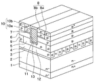
- the SiC semiconductor device according to the present embodiment is a semiconductor element in which an inverted vertical MOSFET having a trench gate structure shown in FIGS. 1 and 2 is formed.
- the vertical MOSFETs shown in these figures are formed in the cell region of the SiC semiconductor device, and the outer periphery withstand voltage structure is formed to surround the cell region, thereby forming the SiC semiconductor device. Only vertical MOSFETs are shown here. In the following, as shown in FIGS.
- the width direction of the vertical MOSFET is X direction
- the depth direction of the vertical MOSFET intersects the X direction is Y direction
- the thickness direction or depth of the vertical MOSFET is The vertical direction, that is, the normal direction to the XY plane is described as the Z direction.
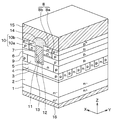
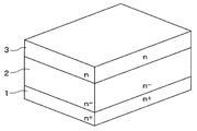
- an n + -type substrate 1 made of SiC is used as a semiconductor substrate in a SiC semiconductor device.
- An n ⁇ -type layer 2 made of SiC is formed on the main surface of the n + -type substrate 1.
- the surface of the n + -type substrate 1 is a (0001) Si plane, and the n-type impurity concentration is, for example, 5.9 ⁇ 10 18 / cm 3 and the thickness is 100 ⁇ m.
- the n ⁇ -type layer 2 has, for example, an n-type impurity concentration of 7.0 ⁇ 10 15 to 1.0 ⁇ 10 16 / cm 3 and a thickness of 8.0 ⁇ m.
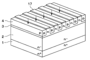
- n - -type layer 2 is formed on the n - -type layer 2, JFET 3 and the field block layer 4 composed of SiC is formed, n - -type layer 2 is connected to the JFET portion 3 at a position away from the n + -type substrate 1 ing.
- the JFET portion 3 and the electric field blocking layer 4 constitute a saturation current suppression layer, and both are extended in the X direction and arranged alternately repeatedly in the Y direction. That is, viewed in the normal direction to the main surface of n + -type substrate 1, at least a part of JFET portion 3 and field blocking layer 4 are each formed into a plurality of strip shapes, that is, stripes. Layout.
- the JFET portion 3 is formed to be lower than the electric field blocking layer 4. Therefore, the stripe-shaped portion of the JFET portion 3 is connected below the electric field blocking layer 4, but each of the stripe-shaped portions is between the plurality of electric field blocking layers 4. It has been placed.
- Each portion of the stripe-shaped portion of the JFET portion 3, that is, each strip-shaped portion, has a width of, for example, 0.25 ⁇ m and a pitch of, for example, 0.6 to 2.0 ⁇ m.
- the thickness of the JFET portion 3 is, for example, 1.5 ⁇ m, and the n-type impurity concentration is higher than that of the n ⁇ -type layer 2 and is, for example, 5.0 ⁇ 10 17 to 2.0 ⁇ 10 18 It is said to be 3 cm 3 .
- the field blocking layer 4 is composed of a p-type impurity layer. As described above, the field blocking layer 4 is in the form of stripes, and each strip-like portion of the field blocking layer 4 in the form of stripes has a width of, for example, 0.15 ⁇ m and a thickness of, for example, 1.4 ⁇ m. ing.
- the electric field blocking layer 4 has a p-type impurity concentration of, for example, 3.0 ⁇ 10 17 to 1.0 ⁇ 10 18 / cm 3 . In the case of the present embodiment, the electric field blocking layer 4 has a constant p-type impurity concentration in the depth direction. In the field blocking layer 4, the surface opposite to the n ⁇ -type layer 2 is flush with the surface of the JFET portion 3.
- an n-type current dispersion layer 5 made of SiC is formed on the JFET portion 3 and the electric field blocking layer 4, an n-type current dispersion layer 5 made of SiC is formed.
- the n-type current dispersion layer 5 is a layer that allows the current flowing through the channel to diffuse in the X direction as described later, and the n-type impurity concentration is higher than, for example, the n ⁇ -type layer 2.
- the n-type current dispersion layer 5 is extended in the Y direction, and the n-type impurity concentration is made equal to or higher than that of the JFET portion 3, for example, the thickness is 0.5 ⁇ m. There is.
- the drift layer is divided into the n ⁇ -type layer 2, the JFET portion 3 and the n-type current dispersion layer 5 for the sake of convenience, they are both parts constituting the drift layer, and It is connected.
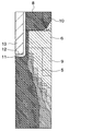
- a p-type base region 6 made of SiC is formed on the n-type current dispersion layer 5. Further, a non-doped layer 7 made of SiC is formed on the p-type base region 6, and an n-type source region 8 is further formed thereon. The n-type source region 8 is formed on a portion of the p-type base region 6 corresponding to the n-type current distribution layer 5.
- the p-type base region 6 is thinner than the field blocking layer 4 and has a low p-type impurity concentration, for example, a p-type impurity concentration of 3 ⁇ 10 17 / cm 3 and a thickness of 0. It is 4 to 0.6 ⁇ m.
- the non-doped layer 7 is a layer not doped with an impurity, or a layer in which the carrier concentration is lowered by doping both an n-type impurity and a p-type impurity.
- the thickness of the non-doped layer 7 is 0.05 to 0.2 ⁇ m.
- the non-doped layer 7 is preferably not doped with both n-type and p-type impurities, but even if doped, the carrier concentration may be 5.0 ⁇ 10 15 / cm 3 or less.
- the non-doped layer 7 has an n-type impurity such as nitrogen (N) of 1.0 ⁇ 10 16 / cm 3 or less, preferably 1.0 ⁇ 10 15 / cm 3 or less.
- the non-doped layer 7 has a p-type impurity such as aluminum (Al) of 1.0 ⁇ 10 16 / cm 3 or less, preferably 1.0 ⁇ 10 15 / cm 3 or less. And, when only one of the p-type impurity and the n-type impurity is doped, the impurity concentration is 5.0 ⁇ 10 15 / cm 3 or less, and when both are doped, they cancel each other. Thus, the carrier concentration is 5.0 ⁇ 10 15 / cm 3 or less.
- Al aluminum
- the n-type source region 8 has a structure in which the n-type impurity concentration is different between the non-doped layer 7 and the p-type base region 6 and the opposite side, that is, the device surface side. Specifically, the n-type source region 8 includes the first source region 8a disposed on the non-doped layer 7 side or the p-type base region 6 side, and the second source region 8b disposed on the element surface side. It is assumed.
- the first source region 8a has an n-type impurity concentration lower than that of the second source region 8b, and is in contact with the non-doped layer 7 in the present embodiment.
- the first source region 8a has, for example, an n-type impurity concentration of 2.0 ⁇ 10 16 to 1.0 ⁇ 10 17 / cm 3 or less and a thickness of 0.2 to 0.5 ⁇ m, preferably 0.3 ⁇ m or more. It is done.
- the second source region 8 b is a region for making contact with the source electrode 15 described later, and has a high concentration of n-type impurities.
- the second source region 8b has, for example, an n-type impurity concentration of 1.0 ⁇ 10 18 to 5.0 ⁇ 10 19 / cm 3 and a thickness of 0.1 to 0.2 ⁇ m.
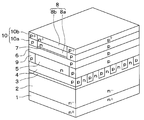
- the p-type deep layer 9 is formed in a portion.
- the p-type deep layer 9 is formed in a strip shape in which the Y direction is a longitudinal direction in a direction intersecting the longitudinal direction of the stripe-shaped portion of the JFET portion 3 and the electric field blocking layer 4. It is laid out in stripes by being arranged in a row in the X direction.
- the p-type base region 6 and the electric field blocking layer 4 are electrically connected through the p-type deep layer 9.
- the formation pitch of the p-type deep layer 9 is matched with the cell pitch as the formation interval of the trench gate structure described later, and the p-type deep layer 9 is disposed between the adjacent trench gate structures.
- the p-type connection layer 10 is formed.
- the p-type connection layer 10 is a layer for electrically connecting by connecting the p-type base region 6 and the source electrode 15 described later.
- the p-type connection layer 10 has a structure in which the p-type impurity concentration is different between the p-type base region 6 side and the opposite side, that is, the element surface side.
- the p-type connection layer 10 is configured to have a first region 10a disposed on the p-type base region 6 side and a second region 10b disposed on the element surface side.
- the first region 10a is configured to be as large as or deeper than the first source region 8a, has a lower p-type impurity concentration than the second region 10b, and has a structure in contact with the p-type base region 6 .
- the first region 10a has, for example, a p-type impurity concentration of 2.0 ⁇ 10 17 to 1.0 ⁇ 10 19 / cm 3 and a thickness of 0.2 to 0.5 ⁇ m, preferably 0.3 ⁇ m or more.
- the carrier concentration that is, the p-type impurity concentration corresponding to the function as a carrier is 2.0 ⁇ 10. It is made to be 17 to 1.0 ⁇ 10 19 / cm 3 .
- the second region 10b is configured to have a depth similar to that of the second source region 8b, and is a region for making contact with the source electrode 15 described later, and has a high concentration of p-type impurities.
- the second region 10b has, for example, a p-type impurity concentration of 2.0 ⁇ 10 18 to 1.0 ⁇ 10 20 / cm 3 and a thickness of 0.2 to 0.3 ⁇ m.
- the carrier concentration that is, the p-type impurity concentration corresponding to the function as a carrier is 2.0 ⁇ 10. It is set to 18 to 1.0 ⁇ 10 20 / cm 3 .
- the p-type connection layer 10 is formed by ion implantation of p-type impurities into the n-type source region 8.
- the p-type impurity concentration of the first region 10a and the second region 10b means the concentration of the p-type impurity that functions as a carrier.
- the n-type impurities contained in the first source region 8a before implantation are canceled and do not function as carriers. Therefore, in the case of forming the p-type connection layer 10 by ion implantation, the dose amount is, for example, 2 to 10 times the n-type impurity concentration of the first source region 8a or the second source region 8b in consideration of the activation rate.
- the width is 0.4 ⁇ m and the depth is p-type base region 6 and n-type source region 8 so as to penetrate n-type source region 8 and p-type base region 6 to reach n-type current distribution layer 5.
- a gate trench 11 is formed 0.2 to 0.4 ⁇ m deeper than the total film thickness.
- the p-type base region 6, the non-doped layer 7 and the n-type source region 8 described above are disposed in contact with the side surfaces of the gate trench 11.
- the gate trench 11 has a strip-like layout in which the X direction in FIG. 2 is the width direction, the direction crossing the longitudinal direction of the JFET portion 3 and the electric field blocking layer 4, here the Y direction is the longitudinal direction and the Z direction is the depth direction.
- the gate trenches 11 are in the form of stripes in which a plurality of the gate trenches 11 are arranged at equal intervals in the X direction, and the p-type base region 6 and the non-doped layer are interposed therebetween. 7 and n-type source regions 8 are arranged. In addition, the p-type deep layer 9 and the p-type connection layer 10 are disposed at an intermediate position of each gate trench 11.
- p-type base region 6 and non-doped layer 7 form a channel region connecting n-type source region 8 and n-type current distribution layer 5 when the vertical MOSFET is operated.
- the inner wall surface of the gate trench 11 including the channel region is covered with a gate insulating film 12.
- a gate electrode 13 made of doped Poly-Si is formed on the surface of the gate insulating film 12, and the inside of the gate trench 11 is completely filled with the gate insulating film 12 and the gate electrode 13 to form a trench gate structure. It is done.
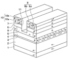
- the source electrode 15 and a gate wiring layer are formed via the interlayer insulating film 14.
- the source electrode 15 and the gate wiring layer are made of a plurality of metals such as Ni / Al.
- at least a portion of the plurality of metals in contact with the n-type SiC, specifically the n-type source region 8 is made of a metal that can make an ohmic contact with the n-type SiC.
- at least a portion of the plurality of metals in contact with the p-type SiC, specifically, the second region 10 b is made of a metal capable of being in ohmic contact with the p-type SiC.
- source electrode 15 is electrically isolated from the SiC portion by being formed on interlayer insulating film 14, n-type source region 8 and p-type are formed through contact holes formed in interlayer insulating film 14. Electrical contact is made with the deep layer 9.
- n + -type substrate 1 On the other hand, on the back side of the n + -type substrate 1 n + -type substrate 1 and electrically connected to the drain electrode 16 are formed.
- Such a structure constitutes an n-channel type inverted trench gate vertical MOSFET.
- a cell region is configured by arranging a plurality of such vertical MOSFETs in a plurality of cells. Then, an outer peripheral withstand voltage structure is formed by a guard ring (not shown) or the like so as to surround a cell region in which such a vertical MOSFET is formed, whereby a SiC semiconductor device is configured.
- the gate voltage Vg of 20 V with respect to the gate electrode 13 is It is made to operate by applying. That is, in the vertical MOSFET, a channel region is formed in the p-type base region 6 and the non-doped layer 7 in a portion in contact with the gate trench 11 by applying the gate voltage Vg. Thereby, the n-type source region 8 and the n-type current distribution layer 5 are electrically connected.
- the vertical MOSFET can further extend from the channel region to the n-type source region 8 through the drift layer formed of the n ⁇ -type layer 2, the JFET portion 3 and the n-type current distribution layer 5 from the n + -type substrate 1. It operates to flow current between drain and source.
- a parasitic diode built in the vertical MOSFET acts as a free wheeling diode.
- a parasitic diode is formed by a PN junction of an n-type layer such as n -- type layer 2 constituting a drift layer and a p-type layer including electric field block layer 4, p-type base region 6 or p-type deep layer 9. And this acts as a freewheeling diode.
- An inverter circuit or the like is used when supplying an alternating current to a load such as an AC motor while using a DC power supply.
- a load such as an AC motor
- a DC power supply for example, a plurality of bridge circuits in which upper and lower arms are connected in series are connected in parallel to a DC power supply, and the upper and lower arms of each bridge circuit are alternately turned on and off alternately. Supply alternating current.
- each bridge circuit such as an inverter circuit
- current is supplied to the load by turning on the vertical MOSFET of the upper arm and turning off the vertical MOSFET of the lower arm. Thereafter, the vertical MOSFETs of the upper arm are turned off, and the vertical MOSFETs of the lower arm are turned on to stop the current supply.
- a parasitic diode provided in the vertical MOSFET on the side to be turned off functions as a freewheeling diode and flows reverse current between source and drain. Do the action. In this way, AC drive of the load by the inverter circuit or the like is performed.
- the n-type source region 8 is configured by the first source region 8 a having a relatively low concentration and the second source region 8 b having a higher concentration than that. Thus, it is possible to reduce the saturation current value at the time of load short circuit. This makes it possible to improve the short circuit withstand capability of the SiC semiconductor device.
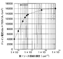
- the electron current density is Examined. 3 and 4 show the respective results. The narrower the hatching interval in the figure, the higher the electron current density. Further, the impurity concentration of the first source region 8a was changed to investigate the change of the drain current. FIG. 5 shows the result.
- the source voltage Vs is 0 V
- the gate voltage Vg is 20 V
- the drain voltage Vd is 750 V.
- the n-type impurity concentration in the entire region of the n-type source region 8 is 1.0 ⁇ 10 19 / cm 3 .
- the n-type impurity concentration of the first source region 8 a is 1.0 ⁇ 10 16 / cm while the n-type source region 8 is formed of the first source region 8 a and the second source region 8 b. 3 and to have the n-type impurity concentration of the second source region 8b and 1.0 ⁇ 10 19 / cm 3.
- the n-type impurity concentration of the second source region 8b is 1.0 ⁇ 10 19 / cm 3 , The n-type impurity concentration of the first source region 8a is changed.
- the n-type source region 8 is formed of the first source region 8a and the second source region 8b, it can be seen that the electron current density is reduced in the first source region 8a. It is considered that this is because the low concentration of the first source region 8a causes depletion so as to enter a wide area of the first source region 8a, and the current does not flow in the depleted portion.
- the saturation current value at the time of load short circuit can be reduced by forming the n-type source region 8 by the first source region 8a and the second source region 8b. Therefore, it is understood that the short circuit withstand capability of the SiC semiconductor device can be improved by adopting the structure of the present embodiment.
- the first source region 8a may have a lower n-type impurity concentration than the second source region 8b, but the saturation current value can not be reduced to a desired value unless the concentration is a certain level. Specifically, if the drain current at the time of load short circuiting is set to 14000 A / cm 2 or less, a desired short circuit withstand voltage can be obtained. Then, as shown in FIG. 5, the reason why the drain current at load shorting is 14000 A / cm 2 or less is that the n-type impurity concentration of the first source region 8 a is 1.0 ⁇ 10 17 / cm 3 or less. That's the case. Therefore, by setting the n-type impurity concentration of the first source region 8a to 1.0 ⁇ 10 17 / cm 3 or less as in the SiC semiconductor device of the present embodiment, it is possible to improve the short circuit withstand voltage.
- the on resistance Ron is preferably 1.2 m ⁇ cm 2 or less. According to the results in FIG.
- the on resistance Ron sharply increases, but if the n-type impurity concentration is higher For example, the on-resistance Ron was less than 1.2 m ⁇ cm 2 . Therefore, as in the SiC semiconductor device of the present embodiment, the deterioration of the on resistance Ron can be suppressed by setting the n-type impurity concentration of the first source region 8a to 2.0 ⁇ 10 16 / cm 3 or more. It becomes.
- n-type impurity concentration of the first source region 8a As described above, by setting the n-type impurity concentration of the first source region 8a to 2.0 ⁇ 10 16 to 1.0 ⁇ 10 17 / cm 3 , deterioration of the on resistance Ron is suppressed while improving the short circuit withstand voltage. It is possible to
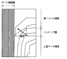
- the non-doped layer 7 is provided between the p-type base region 6 and the first source region 8a. Therefore, the effect of suppressing damage to the gate insulating film 12 can be obtained.
- This effect will be described with reference to FIGS. 7 to 9.
- 7 to 9 each have the non-doped layer 7 when the first source region 8a is formed in contact with the p-type base region 6 when the entire region of the n-type source region 8 has a high impurity concentration.
- the result of investigating the voltage distribution at the time of reverse conduction is shown about the case of the structure of this embodiment. As conditions for reverse conduction, the gate voltage Vg is 20 V, and the drain-source voltage Vds is -5 V.
- a parasitic diode formed in the vertical MOSFET functions as a freewheeling diode, and a freewheeling current flows through the parasitic diode.
- the holes diffused from the p-type layer side of the PN junction constituting the parasitic diode to the n-type layer side recombine with the electrons in the n-type layer.
- BPD basal plane dislocation
- SSSF single Shockley Stacking Fault
- BPD is a linear defect
- the occupied area in the cell region of the SiC semiconductor device is narrow and there is almost no influence on the device operation, but if it is SSSF, the occupied area in the cell region will be a stacked defect. It becomes wider and the influence on the device operation becomes larger. For this reason, if the gate voltage Vg is positively applied even in reverse conduction to form the channel region, and the reflux current flows also through the channel region, it is possible to disperse the reflux current and reduce the recombination energy, It becomes possible to suppress the occurrence of SSSF.
- n-type source region 8 in the case of forming an n-type source region 8 in a high concentration all over so as to be in contact with p-type base region 6, a potential distribution occurs at the PN junction during reverse conduction. A high electric field is applied to the mold source region 8.
- n-type source region 8 When n-type source region 8 is formed to be in contact with p-type base region 6, carriers existing in a portion of n-type source region 8 in contact with p-type base region 6 by an electric field applied to n-type source region 8 It is accelerated by an electric field and becomes hot electrons. This collides with the gate insulating film 12 to cause a problem that the gate insulating film 12 is damaged.
- the n-type impurity concentration is increased in the entire region of the n-type source region 8, this problem becomes remarkable.
- the first source region 8 a when the first source region 8 a is provided in the n-type source region 8 even if the non-doped layer 7 is not provided, a PN junction is formed by the p-type base region 6 and the first source region 8 a.
- the n-type impurity concentration of the first source region 8a is relatively low even if the non-doped layer 7 is not provided. It can be suppressed to some extent. That is, as shown in FIG. 8, the interval of equipotential lines at the PN junction becomes wider than in the case of FIG. 7, and the structure provided with the first source region 8a can suppress the electric field to some extent.
- the non-doped layer 7 is provided between the p-type base region 6 and the first source region 8a as in the present embodiment, as shown in FIG. It is possible to weaken the electric field in the n-type source region 8. Then, although an electric field is generated in the non-doped layer 7, almost no carriers exist in the non-doped layer 7. Therefore, by providing the non-doped layer 7, damage to the gate insulating film 12 due to hot electrons during reverse conduction can be suppressed.
- the SiC semiconductor device of the present embodiment is provided with the JFET portion 3 and the electric field blocking layer 4. Therefore, during operation of the vertical MOSFET, the JFET portion 3 and the electric field block layer 4 function as a saturation current suppression layer, and a structure capable of maintaining a low saturation current while achieving a low on resistance by exerting a saturation current suppression effect. It becomes possible to Specifically, since the stripe-shaped portion of the JFET portion 3 and the electric field blocking layer 4 are alternately formed repeatedly, the following operation is performed.
- the depletion layer extending from the electric field blocking layer 4 side to the JFET portion 3 has a stripe shape in the JFET portion 3 Only the width smaller than the width of the part taken is extended. Therefore, even if the depletion layer extends into JFET portion 3, the current path is secured. Further, since the n-type impurity concentration of the JFET portion 3 is higher than that of the n ⁇ -type layer 2 and the current path can be configured to have a low resistance, it is possible to achieve a low on-resistance.
- the depletion layer extending from the electric field block layer 4 to the JFET portion 3 extends more than the width of the JFET portion 3 in a stripe shape. . Then, the JFET portion 3 is immediately pinched off earlier than the n-type current distribution layer 5. At this time, the relationship between the drain voltage Vd and the width of the depletion layer is determined based on the width of the striped portion of the JFET portion 3 and the n-type impurity concentration.
- the width and n-type impurity concentration of the stripe-shaped portion of the JFET portion 3 are set so that the JFET portion 3 is pinched off when the voltage becomes a little higher than the drain voltage Vd in the normal operation. Do. As a result, the JFET portion 3 can be pinched off even with a low drain voltage Vd. As described above, by causing the JFET unit 3 to be immediately pinched off when the drain voltage Vd becomes higher than the voltage at the time of normal operation, a low saturation current can be maintained, and furthermore, due to a load short circuit or the like. It is possible to improve the withstand voltage of the SiC semiconductor device.
- the JFET portion 3 and the electric field block layer 4 function as a saturation current suppression layer, and by exerting a saturation current suppression effect, a SiC semiconductor device capable of achieving both a low on resistance and a low saturation current can be obtained. It becomes possible.
- the stripe-shaped portion of the JFET portion 3 and the electric field blocking layer 4 are alternately and repeatedly formed. Therefore, even if the drain voltage Vd becomes high, the extension of the depletion layer extending from the lower side to the n -- type layer 2 is suppressed by the electric field block layer 4 and the extension to the trench gate structure is prevented. it can. Therefore, the electric field suppressing effect to reduce the electric field applied to the gate insulating film 12 can be exhibited, and the destruction of the gate insulating film 12 can be suppressed, so that a highly reliable device with high withstand voltage can be obtained. .
- the n-type impurity concentration of the n -- type layer 2 and the JFET portion 3 constituting a part of the drift layer can be made relatively high. It becomes possible to achieve on resistance.
- n + -type substrate 1 is prepared as a semiconductor substrate.
- n -- type layer 2 made of SiC is formed on the main surface of n + -type substrate 1 by epitaxial growth using a CVD (chemical vapor deposition) apparatus (not shown).
- CVD chemical vapor deposition
- a so-called epitaxial substrate may be used in which the n ⁇ -type layer 2 is grown in advance on the main surface of the n + -type substrate 1.
- the JFET portion 3 made of SiC is epitaxially grown on the n ⁇ -type layer 2.
- the epitaxial growth is performed by introducing a gas serving as an n-type dopant, for example, nitrogen gas, in addition to silane and propane serving as a source gas of SiC.
- a gas serving as an n-type dopant for example, nitrogen gas
- silane and propane serving as a source gas of SiC.
- Step shown in FIG. 10B After disposing the mask 17 on the surface of the JFET portion 3, the mask 17 is patterned to open the formation planned region of the electric field blocking layer 4. Then, the electric field blocking layer 4 is formed by ion implantation of a p-type impurity. Thereafter, the mask 17 is removed.
- the electric field blocking layer 4 is formed by ion implantation here, the electric field blocking layer 4 may be formed by a method other than ion implantation. For example, a recess is formed at a position corresponding to the electric field block layer 4 by selectively anisotropically etching the JFET portion 3, and a p-type impurity layer is epitaxially grown thereon, and then the portion is positioned on the JFET portion 3. The p-type impurity layer is flattened in the portion to form the electric field blocking layer 4.
- the field blocking layer 4 can also be formed by epitaxial growth.
- a gas to be a p-type dopant for example, trimethylaluminum (hereinafter referred to as TMA) may be introduced in addition to the raw material gas of SiC.
- TMA trimethylaluminum
- n-type current dispersion layer 5 is formed by epitaxially growing n-type SiC on JFET portion 3 and field blocking layer 4. Then, on the n-type current dispersion layer 5, a mask (not shown) is disposed in which an area for forming the p-type deep layer 9 is opened. Thereafter, a p-type deep layer 9 is formed by ion implantation of p-type impurities from above the mask. Although the p-type deep layer 9 is also formed by ion implantation, it may be formed by a method other than ion implantation.
- the p-type impurity layer is epitaxially grown and then the p-type impurity layer is planarized to form a p-type deep layer. 9 may be formed.
- the p-type base region 6, the non-doped layer 7 and the n-type source region 8 are epitaxially grown in order on the n-type current dispersion layer 5 and the p-type deep layer 9 using a CVD apparatus (not shown).
- a CVD apparatus for example, in the same CVD apparatus, first, the p-type deep layer 9 is formed by epitaxial growth in which a gas to be a p-type dopant is introduced. Subsequently, the non-doped layer 7 is formed by continuously performing epitaxial growth in a state where the introduction of the dopant gas of both the p-type dopant and the n-type dopant is stopped.
- the n-type source region 8 is formed by epitaxial growth in which a gas to be an n-type dopant is introduced.
- the introduction amount of the n-type dopant by adjusting the introduction amount of the n-type dopant, the n-type impurity concentration of the first source region 8a and the second source region 8b is adjusted to a desired value.
- the p-type base region 6, the non-doped layer 7 and the n-type source region 8 can be formed with the above-described impurity concentration and film thickness.
- the film thickness and impurity concentration of each part are determined as follows.
- the film thickness is such that it defines the channel length while setting the impurity concentration to configure the inversion type channel when applying the gate voltage Vg. It is like that. Therefore, for the p-type base region 6, for example, the p-type impurity concentration is 3 ⁇ 10 17 / cm 3 and the thickness is 0.4 to 0.6 ⁇ m.
- the film thickness of the non-doped layer 7 can be set arbitrarily, but if it is too thick, the on resistance Ron becomes high. Therefore, the thickness is 0.05 to 0.2 ⁇ m.
- the non-doped layer 7 basically, it is preferable that no impurity is present, but it is sufficient if the carrier concentration is low.
- the p-type impurity remaining in the atmosphere is introduced or the nitrogen existing in the atmosphere is used as the n-type impurity. It may be introduced. Even in such a case, the impurity concentration should be low.
- the impurity of the other conductivity type is intentionally introduced so that both are doped so that the carrier concentration is canceled out. It should be lowered.
- the impurity concentration is 5.0 ⁇ 10 15 / cm 3 or less, and when both are doped, they cancel each other.
- the carrier concentration is made to be 5.0 ⁇ 10 15 / cm 3 or less.
- the film can be controlled so that the saturation current value can be reduced and the on resistance Ron becomes high. Thickness and n-type impurity concentration are set. Therefore, for the first source region 8a, for example, the n-type impurity concentration is set to 2.0 ⁇ 10 16 to 1.0 ⁇ 10 17 / cm 3 and the thickness is set to 0.2 ⁇ m or more.
- the second source region 8 b of the n-type source region 8 is a film that does not lose its entire area due to a chemical reaction with the source electrode 15 while being in an impurity concentration to be in ohmic contact with the source electrode 15. It is set to thick. The higher the n-type impurity concentration of the second source region 8b, the easier it is to make ohmic contact.
- the n-type source region 8 may be epitaxially grown as in the present embodiment and then p-type impurities may be ion-implanted to form the p-type connection layer 10. In this case, n of the n-type source region 8 is formed. If the type impurity concentration is too high, the p-type connection layer 10 can not have a desired concentration. Therefore, in the case of the present embodiment, the n-type impurity concentration of the second source region 8b is set to, for example, 1.0 ⁇ 10 18 to 5.0 ⁇ 10 19 / cm 3 .
- the source electrode 15 is made of a plurality of metals, and the portion to be in ohmic contact with the second source region 8 b is made of, for example, Ni.
- the second source region 8b to be in contact with Ni becomes an ohmic contact by becoming Ni silicide, but the second source region 8b disappears because it is silicided.
- the thickness of the second source region 8b is set at 0. 2 in order to prevent the entire area of the second source region 8b from disappearing due to the silicidation reaction because the thickness of about 0.1 ⁇ m becomes Ni silicide by the silicidation reaction. It is more than 1 ⁇ m.
- the film thickness of the first source region 8a is 0.5 ⁇ m or less
- the film thickness of the second source region 8b is 0.2 ⁇ m or less.
- the p-type base region 6 When the p-type base region 6, the non-doped layer 7 and the n-type source region 8 are formed by epitaxial growth, the variation in film thickness of each portion can be reduced. Further, with regard to the p-type base region 6 used for forming the channel region, the channel length can be formed with high accuracy by reducing the film thickness variation. This makes it possible to reduce the variation in the threshold Vth of the vertical MOSFET.
- the film thickness of the p-type base region 6 at the time of epitaxial growth needs to be increased in anticipation of the thickness of the non-doped layer 7 and the n-type source region 8 formed by ion implantation.
- the film thickness variation during epitaxial growth increases as the film thickness to be grown becomes thicker, but the variation in ion implantation range is not so large, so the film thickness variation in the p-type base region 6 after ion implantation Variation corresponding to the film thickness.
- the film thickness variation is ⁇ 0.21 ⁇ m when the p-type base region 6 has a thickness of 1.4 ⁇ m, for example, even after the non-doped layer 7 and the n-type source region 8 are formed by ion implantation, the film thickness variation of the p-type base region 6 is ⁇ 0.21 ⁇ m.
- the film thickness variation of the p-type base region 6 corresponds to the variation including the film thickness of the non-doped layer 7 and the n-type source region 8.
- the variation corresponds to the thickness of only the p-type base region 6.
- the film thickness variation is ⁇ 0.06 to 0.09 ⁇ m. Therefore, by forming each portion by epitaxial growth, it is possible to suppress the film thickness variation of the p-type base region 6 and to form the channel length accurately.
- the impurity species and the impurity concentration do not change rapidly because the lattice constant depends on the impurity species and the impurity concentration.
- the impurity species does not immediately change from the p-type to the n-type. Therefore, the impurity species can be prevented from changing rapidly. Further, even when the n-type source region 8 is formed, the relatively low concentration first source region 8a is formed, and then the relatively high concentration second source region 8b is formed. Can not change rapidly.
- a mask (not shown) is disposed on the n-type source region 8 with a position for forming the p-type connection layer 10 open. Then, after ion implantation of p-type impurities from above the mask, heat treatment at 1500 ° C. or higher is performed for activation. As an element to be ion implanted, one or both of boron (B) and aluminum (Al) are used. Thereby, the n-type source region 8 can be turned back by ion implantation of p-type impurities to form the p-type connection layer 10.
- the p-type connection layer 10 needs to be connected to the p-type base region 6, the p-type impurity is also implanted into the non-doped layer 7, and this portion is also implanted with the p-type connection layer 10.
- the second region 10 b of the p-type connection layer 10 needs to be in ohmic contact with the source electrode 15. Therefore, ion implantation is performed at a dose of 2 to 10 times the n-type impurity concentration of the second source region 8b.
- the dose amount if it is twice the n-type impurity concentration of the second source region 8b, it is considered that the carrier concentration can be made such that it can make ohmic contact with the source electrode 15. It is preferable to make it 10 times.
- the carrier concentration of the second region 10b that is, the p-type impurity concentration of the portion serving as a carrier excluding portions canceled or not activated with the second source region 8b is, for example, 2.0 ⁇ . It can be 10 18 to 1.0 ⁇ 10 20 / cm 3 .
- the higher the impurity concentration of the second region 10b the easier the ohmic contact with the source electrode 15 can be made, but the second source region 8b before the second region 10b is formed must also be in ohmic contact with the source electrode 15 .
- a large amount of dose causes generation of crystal defects due to ion implantation, it is necessary to suppress the amount to a certain amount.
- the n-type impurity concentration of the second source region 8b and the p-type impurity concentration of the second region 10b are set to, for example, 1.0 ⁇ 10 18 to 5.0 ⁇ 10 19 / cm 3 .
- the p-type impurity concentration may be lower than that of the second region 10b.
- the p-type impurity is ion-implanted at a dose of 2 to 10 times that of the first source region 8a.
- the total film thickness of the non-doped layer 7 and the n-type source region 8 into which the p-type impurity is implanted is 0.8 ⁇ m or less from the viewpoint of the output of the ion implantation apparatus. It is preferable that In this way, the p-type connection layer 10 can be formed to reach the p-type base region 6 even with the output of a widely used ion implantation apparatus, and mass productivity can be ensured.
- Step shown in FIG. 10F After a mask (not shown) is formed on the n-type source region 8 and the like, a region for forming a gate trench 11 in the mask is opened. Then, anisotropic etching such as RIE (Reactive Ion Etching) is performed using a mask to form the gate trench 11.
- RIE Reactive Ion Etching
- Step shown in FIG. 10G Thereafter, the mask is removed and then thermal oxidation is performed, for example, to form the gate insulating film 12, and the gate insulating film 12 covers the inner wall surface of the gate trench 11 and the surface of the n-type source region 8. Then, after depositing Poly-Si doped with p-type impurities or n-type impurities, this is etched back to leave at least Poly-Si in the gate trench 11, thereby forming the gate electrode 13. This completes the trench gate structure.
- interlayer insulating film 14 formed of, for example, an oxide film or the like is formed to cover the surfaces of gate electrode 13 and gate insulating film 12. Further, contact holes for exposing the n-type source region 8 and the p-type deep layer 9 are formed in the interlayer insulating film 14 using a mask not shown. Then, after an electrode material composed of, for example, a laminated structure of a plurality of metals is formed on the surface of the interlayer insulating film 14, the electrode material is patterned to form the source electrode 15 and the gate wiring layer. Furthermore, the drain electrode 16 is formed on the back surface side of the n + -type substrate 1. Thus, the SiC semiconductor device according to the present embodiment is completed.
- the n-type source region 8 is configured by the first source region 8 a having a relatively low concentration and the second source region 8 b having a higher concentration than that. doing. Therefore, it is possible to reduce the saturation current value at the time of load short circuit, and it is possible to improve the short circuit withstand capacity of the SiC semiconductor device.
- the non-doped layer 7 is provided between the p-type base region 6 and the first source region 8a. As a result, the generation of hot electrons can be suppressed, and the effect that the damage to the gate insulating film 12 can be suppressed can be obtained.
- this is merely an example of the configuration of the vertical MOSFET, and a structure without the JFET portion 3 and the field blocking layer 4, a structure without the n-type current distribution layer 5, or a structure without both of them.
- a structure without the JFET portion 3 and the field blocking layer 4 a structure without the n-type current distribution layer 5, or a structure without both of them.
- the p-type base region 6, the non-doped layer 7 and the n-type source region 8 are formed by epitaxial growth, but may be formed by other methods.
- the variation in channel length may be larger, but the non-doped layer 7 and the n-type source region 8 are formed by ion implanting n-type impurities into the p-type base region 6. Also good.
- the thickness of the n-type source region 8 is added on the p-type base region 6 to epitaxially grow the non-doped layer 7, and the n-type impurity is ion implanted into the non-doped layer 7 to form the n-type source region 8 You may.
- the non-doped layer 7 and the n-type source region 8 are formed by ion implantation, there are parts where the side surfaces of the gate trench 11 are not perpendicular to the surface of the n-type source region 8.
- the gate trench 11 when the gate trench 11 is formed, removal of defects on the inner wall surface is performed by performing sacrificial oxidation or chemical dry etching as necessary, but if there is ion implantation damage, the portion is damaged. It is easier to remove than the non-received part. For this reason, the opening width widens at the entrance side of the gate trench 11, and the side surface of the gate trench 11 does not become perpendicular to the surface of the n-type source region 8. From this point as well, it is preferable to form the non-doped layer 7 and the n-type source region 8 by epitaxial growth.
- the p-type deep layer 9 and the p-type connection layer 10 were comprised separately, you may comprise these with the same p-type layer.
- a deep trench reaching the electric field blocking layer 4 from the surface of the n-type source region 8 through the non-doped layer 7, the p-type base region 6 and the n-type current distribution layer 5 is formed.
- Form a p-type layer In this way, it is possible to form the p-type deep layer 9 and the p-type connection layer 10 by the p-type layer.
- the structure in which the n-type source region 8 is divided into two regions having different impurity concentrations, ie, the first source region 8a and the second source region 8b, has been described. It does not have to be a partitioned structure. That is, the p-type base region 6 side of the n-type source region 8 has a lower impurity concentration than the surface side in contact with the source electrode 15, and the high impurity concentration in which the surface side makes ohmic contact with the source electrode 15. It should be done.
- each impurity layer can be appropriately changed.
- the first region 10a is formed to a position deeper than the first source region 8a
- the second region 10b is formed to a position deeper than the second source region 8b and the non-doped layer 7. May be
- the n-channel vertical MOSFET having the first conductivity type as n-type and the second conductivity type as p-type has been described as an example, but the conductivity type of each component is as follows. It may be a reversed p-channel vertical MOSFET. Further, in the above description, the vertical MOSFET has been described as an example of the semiconductor element, but the present disclosure can also be applied to an IGBT having a similar structure. In the case of an n-channel type IGBT, the conductivity type of the n + -type substrate 1 is merely changed from n-type to p-type in each of the above embodiments, and the other structure and manufacturing method are the same as in the above embodiments. It is.
Abstract
A first conductive source region (8) is configured such that a portion thereof on a second conductive base region (6) side has a lower impurity concentration than a portion thereof on the side of the surface which is brought into ohmic contact with a source electrode (15). For example, the source region (8) is configured such that a first source region (8a) has a relatively low concentration and a second source region (8b) has a higher concentration than the first source region. Thus, a saturation current value during load short-circuiting can be reduced, and the short-circuit capacity of this SiC semiconductor device can be increased.
Description
本出願は、2017年8月31日に出願された日本特許出願番号2017-166883号に基づくもので、ここにその記載内容が参照により組み入れられる。
This application is based on Japanese Patent Application No. 2017-166883 filed on Aug. 31, 2017, the contents of which are incorporated herein by reference.
本開示は、炭化珪素(以下、SiCという)にて構成されるMOS構造の半導体素子を有したSiC半導体装置およびその製造方法に関する。
The present disclosure relates to a SiC semiconductor device having a semiconductor element of a MOS structure formed of silicon carbide (hereinafter referred to as SiC) and a method of manufacturing the same.
従来より、大電流が流せるようにチャネル密度を高くした構造として、トレンチゲート構造を有するSiC半導体装置がある。このSiC半導体装置は、n型ドリフト層の上にp型ベース領域とn+型ソース領域とが順に形成され、n+型ソース領域の表面からp型ベース領域を貫通してn+型ドリフト層に達するようにトレンチゲートが形成された構造とされる。具体的には、n型ドリフト層の上にp型ベース領域をエピタキシャル成長させたのち、p型ベース領域に対してn型不純物をイオン注入で打ち返すことでp型ベース領域の一部をn型に反転させ、n+型ソース領域を形成している。例えば、国際公開第2016/063644号パンフレットを参照。
Conventionally, there is a SiC semiconductor device having a trench gate structure as a structure in which the channel density is increased to allow a large current to flow. In this SiC semiconductor device, a p-type base region and an n + -type source region are sequentially formed on an n-type drift layer, and an n + -type drift layer penetrates the p-type base region from the surface of the n + -type source region. The trench gate is formed in such a way as to reach. Specifically, after the p-type base region is epitaxially grown on the n-type drift layer, a part of the p-type base region is made n-type by ion implantation of n-type impurities against the p-type base region. It is inverted to form an n + -type source region. See, for example, WO 2016/063644.
しかしながら、n+型ソース領域の全域を高濃度のn型不純物層によって形成しているため、負荷短絡時の飽和電流値が大きくなり、SiC半導体装置の短絡耐量を得ることができない。
However, since the entire region of the n + -type source region is formed of the high concentration n-type impurity layer, the saturation current value at the time of load shorting becomes large, and the short circuit resistance of the SiC semiconductor device can not be obtained.
本開示は、短絡耐量を向上することが可能なSiC半導体装置およびその製造方法を提供することを目的とする。
An object of the present disclosure is to provide a SiC semiconductor device capable of improving the short circuit resistance and a method of manufacturing the same.
本開示の1つの観点におけるSiC半導体装置は、SiCで構成された第1または第2導電型の基板と、基板の上に形成され、基板よりも低不純物濃度とされた第1導電型のSiCからなるドリフト層と、ドリフト層の上に形成された第2導電型のSiCからなるベース領域と、ベース領域の上に形成され、ドリフト層よりも第1導電型不純物濃度が高くされた第1導電型のSiCからなるソース領域と、ソース領域の表面からベース領域よりも深く形成されたゲートトレンチ内に、該ゲートトレンチの内壁面を覆うゲート絶縁膜と該ゲート絶縁膜の上に配置されたゲート電極とを備えて構成され、一方向を長手方向として複数本がストライプ状に並べられたトレンチゲート構造と、ゲート電極およびゲート絶縁膜を覆うと共にコンタクトホールが形成された層間絶縁膜と、コンタクトホールを通じて、ソース領域にオーミック接触させられたソース電極と、基板の裏面側に形成されたドレイン電極と、を含む半導体素子を備えている。そして、ソース領域は、ベース領域側の方がソース電極にオーミック接触させられる表面側よりも低不純物濃度で構成されている。
A SiC semiconductor device according to one aspect of the present disclosure includes a first or second conductivity type substrate made of SiC, and a first conductivity type SiC formed on the substrate and having a lower impurity concentration than the substrate. A first conductive type impurity layer formed on the drift region, the base region made of SiC of the second conductive type formed on the drift layer, and the base region, the first conductive type impurity concentration being higher than that of the drift layer; A gate insulating film covering the inner wall surface of the gate trench and a gate insulating film covering the inner wall surface of the source trench made of a conductive type SiC and a gate trench formed deeper than the base region from the surface of the source region A trench gate structure comprising a plurality of gate electrodes arranged in stripes with one direction being a longitudinal direction, a gate electrode and a gate insulating film, and a contact An interlayer insulating film Lumpur is formed, through the contact hole, and includes a source electrode brought into ohmic contact with the source region, and a drain electrode formed on the back surface side of the substrate, a semiconductor device including a. The source region is configured to have a lower impurity concentration on the side of the base region than on the surface side in ohmic contact with the source electrode.
このように、ソース領域のうちのベース領域側を低濃度とし、ソース電極側をそれよりも高濃度としている。このように、ソース領域のうちのベース領域側に低濃度となる領域を備えることで、負荷短絡時の飽和電流値を小さくすることが可能となり、SiC半導体装置の短絡耐量を向上させることが可能となる。
As described above, the base region side of the source region is set to a low concentration, and the source electrode side is set to a concentration higher than that. As described above, by providing the region having a low concentration on the side of the base region in the source region, it is possible to reduce the saturation current value at the time of load short circuit, and it is possible to improve the short circuit withstand capacity of the SiC semiconductor device. It becomes.
なお、各構成要素等に付された括弧付きの参照符号は、その構成要素等と後述する実施形態に記載の具体的な構成要素等との対応関係の一例を示すものである。
The reference numerals in parentheses attached to each component, etc., shows an example of a relationship of the specific component such as described in the following embodiments and their components, and the like.
以下、本開示の実施形態について図に基づいて説明する。なお、以下の各実施形態相互において、互いに同一もしくは均等である部分には、同一符号を付して説明を行う。
Hereinafter, embodiments of the present disclosure will be described based on the drawings. In the following embodiments, parts that are the same as or equivalent to each other will be described with the same reference numerals.
(第1実施形態)
第1実施形態について説明する。本実施形態にかかるSiC半導体装置は、半導体素子として、図1および図2に示すトレンチゲート構造の反転型の縦型MOSFETが形成されたものである。これらの図に示す縦型MOSFETは、SiC半導体装置のうちのセル領域に形成されており、そのセル領域を囲むように外周耐圧構造が形成されることでSiC半導体装置が構成されているが、ここでは縦型MOSFETのみ図示してある。なお、以下では、図1および図2に示すように、縦型MOSFETの幅方向をX方向、X方向に対して交差する縦型MOSFETの奥行方向をY方向、縦型MOSFETの厚み方向もしくは深さ方向、つまりXY平面に対する法線方向をZ方向として説明する。 First Embodiment
The first embodiment will be described. The SiC semiconductor device according to the present embodiment is a semiconductor element in which an inverted vertical MOSFET having a trench gate structure shown in FIGS. 1 and 2 is formed. The vertical MOSFETs shown in these figures are formed in the cell region of the SiC semiconductor device, and the outer periphery withstand voltage structure is formed to surround the cell region, thereby forming the SiC semiconductor device. Only vertical MOSFETs are shown here. In the following, as shown in FIGS. 1 and 2, the width direction of the vertical MOSFET is X direction, the depth direction of the vertical MOSFET intersects the X direction is Y direction, the thickness direction or depth of the vertical MOSFET is The vertical direction, that is, the normal direction to the XY plane is described as the Z direction.
図1および図2に示されるように、SiC半導体装置には、SiCからなるn+型基板1が半導体基板として用いられている。n+型基板1の主表面上にSiCからなるn-型層2が形成されている。n+型基板1は、表面が(0001)Si面とされ、例えばn型不純物濃度が5.9×10¹⁸/cm3とされ、厚さが100μmとされている。n-型層2は、例えばn型不純物濃度が7.0×1015~1.0×1016/cm3とされ、厚さが8.0μmとされている。
As shown in FIGS. 1 and 2, an n + -type substrate 1 made of SiC is used as a semiconductor substrate in a SiC semiconductor device. An n − -type layer 2 made of SiC is formed on the main surface of the n + -type substrate 1. The surface of the n + -type substrate 1 is a (0001) Si plane, and the n-type impurity concentration is, for example, 5.9 × 10 18 / cm 3 and the thickness is 100 μm. The n − -type layer 2 has, for example, an n-type impurity concentration of 7.0 × 10 15 to 1.0 × 10 16 / cm 3 and a thickness of 8.0 μm.
n-型層2の上には、SiCからなるJFET部3と電界ブロック層4が形成されており、n-型層2は、n+型基板1から離れた位置においてJFET部3と連結されている。
on the n - -type layer 2, JFET 3 and the field block layer 4 composed of SiC is formed, n - -type layer 2 is connected to the JFET portion 3 at a position away from the n + -type substrate 1 ing.
JFET部3と電界ブロック層4は、飽和電流抑制層を構成するものであり、共に、X方向に延設され、Y方向において交互に繰り返し並べられて配置されている。つまり、n+型基板1の主表面に対する法線方向から見て、JFET部3の少なくとも一部と電界ブロック層4は、それぞれ複数の短冊状、つまりストライプ状とされ、それぞれが交互に並べられたレイアウトとされている。
The JFET portion 3 and the electric field blocking layer 4 constitute a saturation current suppression layer, and both are extended in the X direction and arranged alternately repeatedly in the Y direction. That is, viewed in the normal direction to the main surface of n + -type substrate 1, at least a part of JFET portion 3 and field blocking layer 4 are each formed into a plurality of strip shapes, that is, stripes. Layout.
なお、本実施形態の場合、JFET部3が電界ブロック層4よりも下方まで形成されたものとされている。このため、JFET部3のうちストライプ状とされている部分は電界ブロック層4の下方において連結した状態になっているが、ストライプ状とされている各部はそれぞれ複数の電界ブロック層4の間に配置された状態となっている。
In the case of this embodiment, the JFET portion 3 is formed to be lower than the electric field blocking layer 4. Therefore, the stripe-shaped portion of the JFET portion 3 is connected below the electric field blocking layer 4, but each of the stripe-shaped portions is between the plurality of electric field blocking layers 4. It has been placed.
JFET部3のうちストライプ状とされている部分の各部、つまり各短冊状の部分は、幅が例えば0.25μm、形成間隔となるピッチが例えば0.6~2.0μmとされている。また、JFET部3の厚みは、例えば1.5μmとされており、n型不純物濃度は、n-型層2よりも高くされていて、例えば5.0×10¹⁷~2.0×10¹⁸/cm3とされている。
Each portion of the stripe-shaped portion of the JFET portion 3, that is, each strip-shaped portion, has a width of, for example, 0.25 μm and a pitch of, for example, 0.6 to 2.0 μm. The thickness of the JFET portion 3 is, for example, 1.5 μm, and the n-type impurity concentration is higher than that of the n − -type layer 2 and is, for example, 5.0 × 10 17 to 2.0 × 10 18 It is said to be 3 cm 3 .
電界ブロック層4は、p型不純物層によって構成されている。上記したように、電界ブロック層4は、ストライプ状とされており、ストライプ状とされた電界ブロック層4の各短冊状の部分は、幅が例えば0.15μm、厚みが例えば1.4μmとされている。また、電界ブロック層4は、例えばp型不純物濃度が3.0×10¹⁷~1.0×10¹⁸/cm3とされている。本実施形態の場合、電界ブロック層4は、深さ方向においてp型不純物濃度が一定とされている。また、電界ブロック層4は、n-型層2と反対側の表面がJFET部3の表面と同一平面とされている。
The field blocking layer 4 is composed of a p-type impurity layer. As described above, the field blocking layer 4 is in the form of stripes, and each strip-like portion of the field blocking layer 4 in the form of stripes has a width of, for example, 0.15 μm and a thickness of, for example, 1.4 μm. ing. The electric field blocking layer 4 has a p-type impurity concentration of, for example, 3.0 × 10 17 to 1.0 × 10 18 / cm 3 . In the case of the present embodiment, the electric field blocking layer 4 has a constant p-type impurity concentration in the depth direction. In the field blocking layer 4, the surface opposite to the n − -type layer 2 is flush with the surface of the JFET portion 3.
さらに、JFET部3および電界ブロック層4の上には、SiCからなるn型電流分散層5が形成されている。n型電流分散層5は、後述するようにチャネルを通じて流れる電流がX方向に拡散できるようにする層であり、例えば、n-型層2よりもn型不純物濃度が高くされている。本実施形態では、n型電流分散層5は、Y方向に向けて延設されており、n型不純物濃度がJFET部3と同じかそれよりも高くされ、例えば厚みが0.5μmとされている。
Furthermore, on the JFET portion 3 and the electric field blocking layer 4, an n-type current dispersion layer 5 made of SiC is formed. The n-type current dispersion layer 5 is a layer that allows the current flowing through the channel to diffuse in the X direction as described later, and the n-type impurity concentration is higher than, for example, the n − -type layer 2. In the present embodiment, the n-type current dispersion layer 5 is extended in the Y direction, and the n-type impurity concentration is made equal to or higher than that of the JFET portion 3, for example, the thickness is 0.5 μm. There is.
なお、ここでは、ドリフト層を、便宜的にn-型層2、JFET部3およびn型電流分散層5に分けて説明しているが、これらは共にドリフト層を構成する部分であり、互いに連結されている。
Here, although the drift layer is divided into the n − -type layer 2, the JFET portion 3 and the n-type current dispersion layer 5 for the sake of convenience, they are both parts constituting the drift layer, and It is connected.
n型電流分散層5の上にはSiCからなるp型ベース領域6が形成されている。また、p型ベース領域6の上には、SiCからなるノンドープ層7が形成され、さらにその上にはn型ソース領域8が形成されている。n型ソース領域8は、p型ベース領域6のうちn型電流分散層5と対応する部分の上に形成されている。
A p-type base region 6 made of SiC is formed on the n-type current dispersion layer 5. Further, a non-doped layer 7 made of SiC is formed on the p-type base region 6, and an n-type source region 8 is further formed thereon. The n-type source region 8 is formed on a portion of the p-type base region 6 corresponding to the n-type current distribution layer 5.
p型ベース領域6は、電界ブロック層4よりも厚みが薄く、かつ、p型不純物濃度が低くされており、例えばp型不純物濃度が3×10¹⁷/cm3とされ、厚さが0.4~0.6μmとされている。
The p-type base region 6 is thinner than the field blocking layer 4 and has a low p-type impurity concentration, for example, a p-type impurity concentration of 3 × 10 17 / cm 3 and a thickness of 0. It is 4 to 0.6 μm.
ノンドープ層7は、不純物をドープしていない層、もしくは、n型不純物およびp型不純物を共にドープすることでキャリア濃度を低くした層である。ノンドープ層7の厚みは、0.05~0.2μmとされている。ノンドープ層7は、n型不純物およびp型不純物が共にドープされていないのが好ましいが、ドープされていたとしても、キャリア濃度が5.0×10¹⁵/cm3以下とされていれば良い。例えば、ノンドープ層7は、窒素(N)などのn型不純物が1.0×1016/cm3以下、好ましくは1.0×1015/cm3以下とされている。また、ノンドープ層7は、アルミニウム(Al)などのp型不純物が1.0×1016/cm3以下、好ましくは1.0×1015/cm3以下とされている。そして、p型不純物とn型不純物の一方のみがドープされている場合には、不純物濃度が5.0×1015/cm3以下とされ、両方がドープされている場合には、互いに打ち消しあうことでキャリア濃度が5.0×1015/cm3以下となっている。
The non-doped layer 7 is a layer not doped with an impurity, or a layer in which the carrier concentration is lowered by doping both an n-type impurity and a p-type impurity. The thickness of the non-doped layer 7 is 0.05 to 0.2 μm. The non-doped layer 7 is preferably not doped with both n-type and p-type impurities, but even if doped, the carrier concentration may be 5.0 × 10 15 / cm 3 or less. For example, the non-doped layer 7 has an n-type impurity such as nitrogen (N) of 1.0 × 10 16 / cm 3 or less, preferably 1.0 × 10 15 / cm 3 or less. The non-doped layer 7 has a p-type impurity such as aluminum (Al) of 1.0 × 10 16 / cm 3 or less, preferably 1.0 × 10 15 / cm 3 or less. And, when only one of the p-type impurity and the n-type impurity is doped, the impurity concentration is 5.0 × 10 15 / cm 3 or less, and when both are doped, they cancel each other. Thus, the carrier concentration is 5.0 × 10 15 / cm 3 or less.
n型ソース領域8は、ノンドープ層7およびp型ベース領域6側とこれらとは反対側、つまり素子表面側とでn型不純物濃度が異なった構造とされている。具体的には、n型ソース領域8は、ノンドープ層7やp型ベース領域6側に配置された第1ソース領域8aと、素子表面側に配置された第2ソース領域8bとを有した構成とされている。
The n-type source region 8 has a structure in which the n-type impurity concentration is different between the non-doped layer 7 and the p-type base region 6 and the opposite side, that is, the device surface side. Specifically, the n-type source region 8 includes the first source region 8a disposed on the non-doped layer 7 side or the p-type base region 6 side, and the second source region 8b disposed on the element surface side. It is assumed.
第1ソース領域8aは、第2ソース領域8bよりもn型不純物濃度が低くされており、本実施形態の場合はノンドープ層7と接している。第1ソース領域8aは、例えばn型不純物濃度が2.0×10¹⁶~1.0×10¹⁷/cm3以下とされ、厚みが0.2~0.5μm、好ましくは0.3μm以上とされている。
The first source region 8a has an n-type impurity concentration lower than that of the second source region 8b, and is in contact with the non-doped layer 7 in the present embodiment. The first source region 8a has, for example, an n-type impurity concentration of 2.0 × 10 16 to 1.0 × 10 17 / cm 3 or less and a thickness of 0.2 to 0.5 μm, preferably 0.3 μm or more. It is done.
第2ソース領域8bは、後述するソース電極15とのコンタクトを取るための領域であり、n型不純物が高濃度とされている。第2ソース領域8bは、例えばn型不純物濃度が1.0×10¹⁸~5.0×10¹⁹/cm3とされ、厚みが0.1~0.2μmとされている。
The second source region 8 b is a region for making contact with the source electrode 15 described later, and has a high concentration of n-type impurities. The second source region 8b has, for example, an n-type impurity concentration of 1.0 × 10 18 to 5.0 × 10 19 / cm 3 and a thickness of 0.1 to 0.2 μm.
また、p型ベース領域6から下方に向けて、具体的にはJFET部3と電界ブロック層4の表面からp型ベース領域6の間であって、n型電流分散層5が形成されていない部分に、p型ディープ層9が形成されている。本実施形態では、p型ディープ層9は、JFET部3のうちのストライプ状の部分や電界ブロック層4の長手方向に対して交差する方向、ここではY方向を長手方向とした短冊状とされ、X方向に複数本並べられることでストライプ状にレイアウトされている。このp型ディープ層9を通じて、p型ベース領域6や電界ブロック層4が電気的に接続されている。p型ディープ層9の形成ピッチは、後述するトレンチゲート構造の形成間隔となるセルピッチと合わせてあり、隣り合うトレンチゲート構造の間にp型ディープ層9が配置されるようにしてある。
Further, from the p-type base region 6 downward, specifically, between the surface of the JFET portion 3 and the field blocking layer 4 to the p-type base region 6, the n-type current dispersion layer 5 is not formed. The p-type deep layer 9 is formed in a portion. In the present embodiment, the p-type deep layer 9 is formed in a strip shape in which the Y direction is a longitudinal direction in a direction intersecting the longitudinal direction of the stripe-shaped portion of the JFET portion 3 and the electric field blocking layer 4. It is laid out in stripes by being arranged in a row in the X direction. The p-type base region 6 and the electric field blocking layer 4 are electrically connected through the p-type deep layer 9. The formation pitch of the p-type deep layer 9 is matched with the cell pitch as the formation interval of the trench gate structure described later, and the p-type deep layer 9 is disposed between the adjacent trench gate structures.
さらに、p型ベース領域6上のうちp型ディープ層9と対応する位置、換言すればn型ソース領域8と異なる位置であってn型ソース領域8を挟んでトレンチゲート構造と反対側の位置に、p型連結層10が形成されている。p型連結層10は、p型ベース領域6と後述するソース電極15とを連結することで電気的に接続するための層である。本実施形態では、p型連結層10は、p型ベース領域6側とその反対側、つまり素子表面側とでp型不純物濃度が異なった構造とされている。具体的には、p型連結層10は、p型ベース領域6側に配置された第1領域10aと、素子表面側に配置された第2領域10bとを有した構成とされている。
Furthermore, a position on p-type base region 6 corresponding to p-type deep layer 9, in other words, a position different from n-type source region 8 and opposite to the trench gate structure with n-type source region 8 interposed. The p-type connection layer 10 is formed. The p-type connection layer 10 is a layer for electrically connecting by connecting the p-type base region 6 and the source electrode 15 described later. In the present embodiment, the p-type connection layer 10 has a structure in which the p-type impurity concentration is different between the p-type base region 6 side and the opposite side, that is, the element surface side. Specifically, the p-type connection layer 10 is configured to have a first region 10a disposed on the p-type base region 6 side and a second region 10b disposed on the element surface side.
第1領域10aは、第1ソース領域8aと同程度もしくは、より深く構成され、第2領域10bよりもp型不純物濃度が低くされていて、p型ベース領域6と接した構造とされている。第1領域10aは、例えばp型不純物濃度が2.0×10¹⁷~1.0×10¹⁹/cm3とされ、厚みが0.2~0.5μm、好ましくは0.3μm以上とされている。ただし、本実施形態の場合、第1領域10aを第1ソース領域8aへのイオン注入によって形成していることから、キャリア濃度、つまりキャリアとして機能する分のp型不純物濃度が2.0×1017~1.0×1019/cm3となるようにしている。
The first region 10a is configured to be as large as or deeper than the first source region 8a, has a lower p-type impurity concentration than the second region 10b, and has a structure in contact with the p-type base region 6 . The first region 10a has, for example, a p-type impurity concentration of 2.0 × 10 17 to 1.0 × 10 19 / cm 3 and a thickness of 0.2 to 0.5 μm, preferably 0.3 μm or more. There is. However, in the case of this embodiment, since the first region 10a is formed by ion implantation into the first source region 8a, the carrier concentration, that is, the p-type impurity concentration corresponding to the function as a carrier is 2.0 × 10. It is made to be 17 to 1.0 × 10 19 / cm 3 .
第2領域10bは、第2ソース領域8bと同程度の深さで構成され、後述するソース電極15とのコンタクトを取るための領域であり、p型不純物が高濃度とされている。第2領域10bは、例えばp型不純物濃度が2.0×10¹⁸~1.0×10²⁰/cm3とされ、厚みが0.2~0.3μmとされている。ただし、本実施形態の場合、第2領域10bを第2ソース領域8bへのイオン注入によって形成していることから、キャリア濃度、つまりキャリアとして機能する分のp型不純物濃度が2.0×1018~1.0×1020/cm3となるようにしている。
The second region 10b is configured to have a depth similar to that of the second source region 8b, and is a region for making contact with the source electrode 15 described later, and has a high concentration of p-type impurities. The second region 10b has, for example, a p-type impurity concentration of 2.0 × 10 18 to 1.0 × 10 20 / cm 3 and a thickness of 0.2 to 0.3 μm. However, in the case of this embodiment, since the second region 10b is formed by ion implantation into the second source region 8b, the carrier concentration, that is, the p-type impurity concentration corresponding to the function as a carrier is 2.0 × 10. It is set to 18 to 1.0 × 10 20 / cm 3 .
なお、後述するように、本実施形態では、n型ソース領域8へのp型不純物のイオン注入によってp型連結層10を形成している。その場合、第1領域10aや第2領域10bのp型不純物濃度は、p型不純物のうちキャリアとして機能する分の濃度のことを意味する。p型不純物のうち、打ち込み前の第1ソース領域8aに含まれているn型不純物とキャンセルされて、キャリアとしては機能しない。このため、イオン注入によってp型連結層10を形成する場合、活性化率を加味して、例えば第1ソース領域8aや第2ソース領域8bのn型不純物濃度の2~10倍のドーズ量でp型不純物を注入すれば、上記したp型不純物濃度が得られる。
As described later, in the present embodiment, the p-type connection layer 10 is formed by ion implantation of p-type impurities into the n-type source region 8. In that case, the p-type impurity concentration of the first region 10a and the second region 10b means the concentration of the p-type impurity that functions as a carrier. Among the p-type impurities, the n-type impurities contained in the first source region 8a before implantation are canceled and do not function as carriers. Therefore, in the case of forming the p-type connection layer 10 by ion implantation, the dose amount is, for example, 2 to 10 times the n-type impurity concentration of the first source region 8a or the second source region 8b in consideration of the activation rate. By implanting a p-type impurity, the above-described p-type impurity concentration can be obtained.
さらに、n型ソース領域8およびp型ベース領域6を貫通してn型電流分散層5に達するように、例えば幅が0.4μm、深さがp型ベース領域6とn型ソース領域8の合計膜厚よりも0.2~0.4μm深くされたゲートトレンチ11が形成されている。このゲートトレンチ11の側面と接するように上述したp型ベース領域6やノンドープ層7およびn型ソース領域8が配置されている。ゲートトレンチ11は、図2のX方向を幅方向、JFET部3や電界ブロック層4の長手方向と交差する方向、ここではY方向を長手方向、Z方向を深さ方向とする短冊状のレイアウトで形成されている。そして、図1および図2には示していないが、ゲートトレンチ11は、複数本がX方向に等間隔に配置されたストライプ状とされており、それぞれの間にp型ベース領域6やノンドープ層7およびn型ソース領域8が配置されている。また、各ゲートトレンチ11の中間位置に、p型ディープ層9やp型連結層10が配置されている。
Further, for example, the width is 0.4 μm and the depth is p-type base region 6 and n-type source region 8 so as to penetrate n-type source region 8 and p-type base region 6 to reach n-type current distribution layer 5. A gate trench 11 is formed 0.2 to 0.4 μm deeper than the total film thickness. The p-type base region 6, the non-doped layer 7 and the n-type source region 8 described above are disposed in contact with the side surfaces of the gate trench 11. The gate trench 11 has a strip-like layout in which the X direction in FIG. 2 is the width direction, the direction crossing the longitudinal direction of the JFET portion 3 and the electric field blocking layer 4, here the Y direction is the longitudinal direction and the Z direction is the depth direction. It is formed of Although not shown in FIGS. 1 and 2, the gate trenches 11 are in the form of stripes in which a plurality of the gate trenches 11 are arranged at equal intervals in the X direction, and the p-type base region 6 and the non-doped layer are interposed therebetween. 7 and n-type source regions 8 are arranged. In addition, the p-type deep layer 9 and the p-type connection layer 10 are disposed at an intermediate position of each gate trench 11.
このゲートトレンチ11の側面の位置において、p型ベース領域6およびノンドープ層7は、縦型MOSFETの作動時にn型ソース領域8とn型電流分散層5との間を繋ぐチャネル領域を形成する。このチャネル領域を含むゲートトレンチ11の内壁面は、ゲート絶縁膜12で覆われている。ゲート絶縁膜12の表面にはドープドPoly-Siにて構成されたゲート電極13が形成されており、これらゲート絶縁膜12およびゲート電極13によってゲートトレンチ11内が埋め尽くされ、トレンチゲート構造が構成されている。
At the position of the side surface of gate trench 11, p-type base region 6 and non-doped layer 7 form a channel region connecting n-type source region 8 and n-type current distribution layer 5 when the vertical MOSFET is operated. The inner wall surface of the gate trench 11 including the channel region is covered with a gate insulating film 12. A gate electrode 13 made of doped Poly-Si is formed on the surface of the gate insulating film 12, and the inside of the gate trench 11 is completely filled with the gate insulating film 12 and the gate electrode 13 to form a trench gate structure. It is done.
また、n型ソース領域8の表面やゲート電極13の表面には、層間絶縁膜14を介してソース電極15や図示しないゲート配線層などが形成されている。ソース電極15やゲート配線層は、複数の金属、例えばNi/Al等にて構成されている。そして、複数の金属のうち少なくともn型SiC、具体的にはn型ソース領域8と接触する部分は、n型SiCとオーミック接触可能な金属で構成されている。また、複数の金属のうち少なくともp型SiC、具体的には第2領域10bと接触する部分は、p型SiCとオーミック接触可能な金属で構成されている。なお、ソース電極15は、層間絶縁膜14上に形成されることでSiC部分と電気的に絶縁されているが、層間絶縁膜14に形成されたコンタクトホールを通じて、n型ソース領域8およびp型ディープ層9と電気的に接触させられている。
Further, on the surface of the n-type source region 8 and the surface of the gate electrode 13, the source electrode 15 and a gate wiring layer (not shown) are formed via the interlayer insulating film 14. The source electrode 15 and the gate wiring layer are made of a plurality of metals such as Ni / Al. Then, at least a portion of the plurality of metals in contact with the n-type SiC, specifically the n-type source region 8 is made of a metal that can make an ohmic contact with the n-type SiC. Further, at least a portion of the plurality of metals in contact with the p-type SiC, specifically, the second region 10 b is made of a metal capable of being in ohmic contact with the p-type SiC. Although source electrode 15 is electrically isolated from the SiC portion by being formed on interlayer insulating film 14, n-type source region 8 and p-type are formed through contact holes formed in interlayer insulating film 14. Electrical contact is made with the deep layer 9.
一方、n+型基板1の裏面側にはn+型基板1と電気的に接続されたドレイン電極16が形成されている。このような構造により、nチャネルタイプの反転型のトレンチゲート構造の縦型MOSFETが構成されている。このような縦型MOSFETが複数セル配置されることでセル領域が構成されている。そして、このような縦型MOSFETが形成されたセル領域を囲むように図示しないガードリングなどによる外周耐圧構造が構成されることでSiC半導体装置が構成されている。
On the other hand, on the back side of the n + -type substrate 1 n + -type substrate 1 and electrically connected to the drain electrode 16 are formed. Such a structure constitutes an n-channel type inverted trench gate vertical MOSFET. A cell region is configured by arranging a plurality of such vertical MOSFETs in a plurality of cells. Then, an outer peripheral withstand voltage structure is formed by a guard ring (not shown) or the like so as to surround a cell region in which such a vertical MOSFET is formed, whereby a SiC semiconductor device is configured.
このように構成される縦型MOSFETを有するSiC半導体装置は、例えば、ソース電圧Vsを0V、ドレイン電圧Vdを1~1.5Vとした状態で、ゲート電極13に対して20Vのゲート電圧Vgを印加することで動作させられる。すなわち、縦型MOSFETは、ゲート電圧Vgが印加されることにより、ゲートトレンチ11に接する部分のp型ベース領域6およびノンドープ層7にチャネル領域を形成する。これにより、n型ソース領域8とn型電流分散層5との間が導通する。したがって、縦型MOSFETは、n+型基板1より、n-型層2とJFET部3およびn型電流分散層5にて構成されるドリフト層を通じ、さらにチャネル領域からn型ソース領域8を通じて、ドレイン-ソース間に電流を流すという動作を行う。
In the SiC semiconductor device having the vertical MOSFET configured in this way, for example, with the source voltage Vs of 0 V and the drain voltage Vd of 1 to 1.5 V, the gate voltage Vg of 20 V with respect to the gate electrode 13 is It is made to operate by applying. That is, in the vertical MOSFET, a channel region is formed in the p-type base region 6 and the non-doped layer 7 in a portion in contact with the gate trench 11 by applying the gate voltage Vg. Thereby, the n-type source region 8 and the n-type current distribution layer 5 are electrically connected. Therefore, the vertical MOSFET can further extend from the channel region to the n-type source region 8 through the drift layer formed of the n − -type layer 2, the JFET portion 3 and the n-type current distribution layer 5 from the n + -type substrate 1. It operates to flow current between drain and source.
また、このような半導体装置における縦型MOSFETを上アームと下アームそれぞれに配置したインバータ回路等に適用すると、縦型MOSFETに内蔵される寄生ダイオードが還流ダイオードとして働く。具体的には、n-型層2などドリフト層を構成するn型層と電界ブロック層4やp型ベース領域6もしくはp型ディープ層9を含むp型層とによるPN接合によって寄生ダイオードが構成され、これが還流ダイオードとして働く。
In addition, when the vertical MOSFET in such a semiconductor device is applied to an inverter circuit or the like arranged in each of the upper arm and the lower arm, a parasitic diode built in the vertical MOSFET acts as a free wheeling diode. Specifically, a parasitic diode is formed by a PN junction of an n-type layer such as n -- type layer 2 constituting a drift layer and a p-type layer including electric field block layer 4, p-type base region 6 or p-type deep layer 9. And this acts as a freewheeling diode.
インバータ回路等は、直流電源を用いつつ交流モータ等の負荷に対して交流電流を供給する際に用いられる。例えば、インバータ回路等は、直流電源に対して上アームと下アームを直列接続したブリッジ回路を複数個並列接続し、各ブリッジ回路の上アームと下アームを交互に繰り返しオンオフさせることで、負荷に対して交流電流を供給する。
An inverter circuit or the like is used when supplying an alternating current to a load such as an AC motor while using a DC power supply. For example, in the inverter circuit etc., a plurality of bridge circuits in which upper and lower arms are connected in series are connected in parallel to a DC power supply, and the upper and lower arms of each bridge circuit are alternately turned on and off alternately. Supply alternating current.
具体的には、インバータ回路等の各ブリッジ回路では、上アームの縦型MOSFETをオン、下アームの縦型MOSFETをオフすることで負荷に対して電流供給を行う。その後、上アームの縦型MOSFETをオフ、下アームの縦型MOSFETをオンして電流供給を停止する。また、各アームの縦型MOSFETのオンオフの切り替えの際には、オフされる側の縦型MOSFETに備えられる寄生ダイオードが還流ダイオードとして働き、還流電流をソース-ドレイン間に流すという逆導通時の動作を行う。このようにして、インバータ回路等による負荷の交流駆動が行われる。
Specifically, in each bridge circuit such as an inverter circuit, current is supplied to the load by turning on the vertical MOSFET of the upper arm and turning off the vertical MOSFET of the lower arm. Thereafter, the vertical MOSFETs of the upper arm are turned off, and the vertical MOSFETs of the lower arm are turned on to stop the current supply. In addition, at the time of switching on and off of the vertical MOSFETs of each arm, a parasitic diode provided in the vertical MOSFET on the side to be turned off functions as a freewheeling diode and flows reverse current between source and drain. Do the action. In this way, AC drive of the load by the inverter circuit or the like is performed.
このような動作を行うに当たり、負荷短絡が発生すると、例えば600~1200Vもしくはそれ以上の電圧がドレイン-ソース間電圧Vdsとしてドレインに印加されることになる。このとき、n型ソース領域8の全域が高濃度のn型不純物層によって構成されていると、負荷短絡時の飽和電流値が大きくなり、SiC半導体装置の短絡耐量を得ることができなくなる。しかしながら、本実施形態のSiC半導体装置では、n型ソース領域8を比較的低濃度とされた第1ソース領域8aとそれよりも高濃度とされた第2ソース領域8bとによって構成していることから、負荷短絡時の飽和電流値を小さくすることが可能となる。これにより、SiC半導体装置の短絡耐量を向上させることが可能となる。
In performing such an operation, when a load short circuit occurs, a voltage of, for example, 600 to 1200 V or more is applied to the drain as the drain-source voltage Vds. At this time, if the entire region of the n-type source region 8 is formed of a high concentration n-type impurity layer, the saturation current value at the time of load shorting becomes large, and the short circuit capacity of the SiC semiconductor device can not be obtained. However, in the SiC semiconductor device of the present embodiment, the n-type source region 8 is configured by the first source region 8 a having a relatively low concentration and the second source region 8 b having a higher concentration than that. Thus, it is possible to reduce the saturation current value at the time of load short circuit. This makes it possible to improve the short circuit withstand capability of the SiC semiconductor device.
ここで、シミュレーションにより、n型ソース領域8の全域を高濃度とした場合と、本実施形態のように第1ソース領域8aおよび第2ソース領域8bで構成した場合、それぞれについて、電子電流密度を調べた。図3および図4は、それぞれの結果を示した図である。図中ハッチングの間隔が狭い部分ほど、電子電流密度が高いことを示している。また、第1ソース領域8aの不純物濃度を変化させて、ドレイン電流の変化を調べた。図5は、その結果を示している。
Here, according to the simulation, when the entire region of the n-type source region 8 has a high concentration and when the first source region 8a and the second source region 8b are configured as in this embodiment, the electron current density is Examined. 3 and 4 show the respective results. The narrower the hatching interval in the figure, the higher the electron current density. Further, the impurity concentration of the first source region 8a was changed to investigate the change of the drain current. FIG. 5 shows the result.
なお、図3~図5のシミュレーションでは、ソース電圧Vsを0V、ゲート電圧Vgを20V、ドレイン電圧Vdを750Vとしている。また、図3のシミュレーションでは、n型ソース領域8の全域のn型不純物濃度を1.0×10¹⁹/cm3としている。同様に、図4のシミュレーションでは、n型ソース領域8を第1ソース領域8aと第2ソース領域8bで構成しつつ、第1ソース領域8aのn型不純物濃度を1.0×1016/cm3とし、第2ソース領域8bのn型不純物濃度を1.0×1019/cm3としている。図5のシミュレーションでは、n型ソース領域8を第1ソース領域8aと第2ソース領域8bで構成しつつ、第2ソース領域8bのn型不純物濃度を1.0×1019/cm3とし、第1ソース領域8aのn型不純物濃度を変化させている。
In the simulations of FIGS. 3 to 5, the source voltage Vs is 0 V, the gate voltage Vg is 20 V, and the drain voltage Vd is 750 V. Further, in the simulation of FIG. 3, the n-type impurity concentration in the entire region of the n-type source region 8 is 1.0 × 10 19 / cm 3 . Similarly, in the simulation of FIG. 4, the n-type impurity concentration of the first source region 8 a is 1.0 × 10 16 / cm while the n-type source region 8 is formed of the first source region 8 a and the second source region 8 b. 3 and to have the n-type impurity concentration of the second source region 8b and 1.0 × 10 19 / cm 3. In the simulation of FIG. 5, while the n-type source region 8 is composed of the first source region 8a and the second source region 8b, the n-type impurity concentration of the second source region 8b is 1.0 × 10 19 / cm 3 , The n-type impurity concentration of the first source region 8a is changed.
図3に示すように、n型ソース領域8の全域のn型不純物濃度を高濃度とした場合、n型ソース領域8の全域において電子電流密度が高くなっていることが判る。これは、n型ソース領域8が高濃度とされていることから、殆ど空乏化する領域が発生せず、n型ソース領域8の全域において電流が流れているためと考えられる。
As shown in FIG. 3, when the n-type impurity concentration in the entire region of the n-type source region 8 is high, it can be seen that the electron current density is high in the entire region of the n-type source region 8. It is considered that this is because the n-type source region 8 has a high concentration, a region to be depleted is hardly generated, and current flows in the entire region of the n-type source region 8.
一方、図4に示すように、n型ソース領域8を第1ソース領域8aおよび第2ソース領域8bで構成した場合、第1ソース領域8aにおいて、電子電流密度が小さくなっていることが判る。これは、第1ソース領域8aが低濃度とされていることから、第1ソース領域8aの広範囲に入り込むように空乏化が生じ、空乏化した部分において電流が流れなくなるためと考えられる。
On the other hand, as shown in FIG. 4, when the n-type source region 8 is formed of the first source region 8a and the second source region 8b, it can be seen that the electron current density is reduced in the first source region 8a. It is considered that this is because the low concentration of the first source region 8a causes depletion so as to enter a wide area of the first source region 8a, and the current does not flow in the depleted portion.
このシミュレーション結果からも、n型ソース領域8を第1ソース領域8aおよび第2ソース領域8bによって構成することで、負荷短絡時における飽和電流値を低減できると言える。したがって、本実施形態の構造とすることで、SiC半導体装置の短絡耐量を向上させることが可能になることが判る。
Also from this simulation result, it can be said that the saturation current value at the time of load short circuit can be reduced by forming the n-type source region 8 by the first source region 8a and the second source region 8b. Therefore, it is understood that the short circuit withstand capability of the SiC semiconductor device can be improved by adopting the structure of the present embodiment.
また、第1ソース領域8aについては、第2ソース領域8bよりもn型不純物濃度が低ければ良いものの、ある程度の濃度でないと飽和電流値を所望値まで低下させることができない。具体的には、負荷短絡時のドレイン電流が14000A/cm2以下となるようにすれば、所望の短絡耐量を得ることができる。そして、図5に示されるように、負荷短絡時のドレイン電流が14000A/cm2以下となるのは、第1ソース領域8aのn型不純物濃度が1.0×1017/cm3以下となる場合である。したがって、本実施形態のSiC半導体装置のように、第1ソース領域8aのn型不純物濃度を1.0×1017/cm3以下とすることで、短絡耐量を向上させることが可能となる。
The first source region 8a may have a lower n-type impurity concentration than the second source region 8b, but the saturation current value can not be reduced to a desired value unless the concentration is a certain level. Specifically, if the drain current at the time of load short circuiting is set to 14000 A / cm 2 or less, a desired short circuit withstand voltage can be obtained. Then, as shown in FIG. 5, the reason why the drain current at load shorting is 14000 A / cm 2 or less is that the n-type impurity concentration of the first source region 8 a is 1.0 × 10 17 / cm 3 or less. That's the case. Therefore, by setting the n-type impurity concentration of the first source region 8a to 1.0 × 10 17 / cm 3 or less as in the SiC semiconductor device of the present embodiment, it is possible to improve the short circuit withstand voltage.
ただし、第1ソース領域8aのn型不純物濃度が低すぎると、第1ソース領域8aの抵抗値が大きくなり過ぎ、オン抵抗Ronを増大させることになる。第1ソース領域8aのn型不純物濃度とオン抵抗Ronとの関係について調べたところ、図6に示す結果となった。SiC半導体装置の高速スイッチング動作を鑑みると、オン抵抗Ronについては1.2mΩcm2以下であることが好ましい。図6の結果によれば、第1ソース領域8aのn型不純物濃度が2.0×10¹⁶/cm3未満になると急激にオン抵抗Ronが上昇するが、n型不純物濃度がそれ以上であれば、オン抵抗Ronを1.2mΩcm2以下にできていた。したがって、本実施形態のSiC半導体装置のように、第1ソース領域8aのn型不純物濃度を2.0×1016/cm3以上とすることで、オン抵抗Ronの劣化を抑制することが可能となる。
However, when the n-type impurity concentration of the first source region 8a is too low, the resistance value of the first source region 8a becomes too large, and the on-resistance Ron increases. The relationship between the n-type impurity concentration of the first source region 8 a and the on-resistance Ron was investigated, and the result is shown in FIG. In view of the high speed switching operation of the SiC semiconductor device, the on resistance Ron is preferably 1.2 mΩcm 2 or less. According to the results in FIG. 6, when the n-type impurity concentration of the first source region 8a is less than 2.0 × 10 16 / cm 3 , the on resistance Ron sharply increases, but if the n-type impurity concentration is higher For example, the on-resistance Ron was less than 1.2 mΩcm 2 . Therefore, as in the SiC semiconductor device of the present embodiment, the deterioration of the on resistance Ron can be suppressed by setting the n-type impurity concentration of the first source region 8a to 2.0 × 10 16 / cm 3 or more. It becomes.
このように、第1ソース領域8aのn型不純物濃度を2.0×10¹⁶~1.0×10¹⁷/cm3とすることで、短絡耐量を向上させつつ、オン抵抗Ronの劣化を抑制することが可能となる。
As described above, by setting the n-type impurity concentration of the first source region 8a to 2.0 × 10 16 to 1.0 × 10 17 / cm 3 , deterioration of the on resistance Ron is suppressed while improving the short circuit withstand voltage. It is possible to
さらに、本実施形態のSiC半導体装置では、p型ベース領域6と第1ソース領域8aとの間にノンドープ層7を備えるようにしている。このため、ゲート絶縁膜12へのダメージを抑制できるという効果が得られる。この効果について、図7~図9を参照して説明する。なお、図7~図9は、それぞれ、n型ソース領域8の全域を高不純物濃度とした場合、第1ソース領域8aをp型ベース領域6に接するように形成した場合、ノンドープ層7を備えた本実施形態の構造の場合について、逆導通時の電圧分布を調べた結果を示している。逆導通時の条件としては、ゲート電圧Vgを20V、ドレイン-ソース間電圧Vdsを-5Vとしている。
Furthermore, in the SiC semiconductor device of the present embodiment, the non-doped layer 7 is provided between the p-type base region 6 and the first source region 8a. Therefore, the effect of suppressing damage to the gate insulating film 12 can be obtained. This effect will be described with reference to FIGS. 7 to 9. 7 to 9 each have the non-doped layer 7 when the first source region 8a is formed in contact with the p-type base region 6 when the entire region of the n-type source region 8 has a high impurity concentration. The result of investigating the voltage distribution at the time of reverse conduction is shown about the case of the structure of this embodiment. As conditions for reverse conduction, the gate voltage Vg is 20 V, and the drain-source voltage Vds is -5 V.
逆通電時には、基本的には、縦型MOSFETに形成される寄生ダイオードが還流ダイオードとして働き、寄生ダイオードを通じて還流電流が流れる。そして、寄生ダイオードを構成するPN接合のp型層側からn型層側に拡散した正孔とn型層中の電子が再結合する。このとき、再結合エネルギーが大きいために、エピタキシャル膜で構成されたn型層中の基底面転位(以下、BPDという)が拡張してシングルショックレースタッキングフォルト(以下、SSSFという)という積層欠陥になる。BPDは線状欠陥であるために、SiC半導体装置のセル領域内における占有面積が狭く、素子動作に及ぼす影響が殆ど無いが、SSSFになると、積層欠陥となるためにセル領域内における占有面積が広くなり、素子動作に及ぼす影響が大きくなる。このため、逆導通時にも積極的にゲート電圧Vgを印加してチャネル領域を形成し、チャネル領域を通じても還流電流が流れるようにすれば、還流電流を分散して再結合エネルギーを低減できるため、SSSFの発生を抑制することが可能となる。ただし、チャネル領域を通じての還流電流の流れが発生することから、p型ベース領域6とn型ソース領域8の間において、高い電界が掛かることになり、ホットエレクトロンを生じさせ、ゲート絶縁膜12にダメージを与えるという現象が発生する。
In reverse conduction, basically, a parasitic diode formed in the vertical MOSFET functions as a freewheeling diode, and a freewheeling current flows through the parasitic diode. Then, the holes diffused from the p-type layer side of the PN junction constituting the parasitic diode to the n-type layer side recombine with the electrons in the n-type layer. At this time, since the recombination energy is large, the basal plane dislocation (hereinafter referred to as BPD) in the n-type layer formed of the epitaxial film is extended to a stacking fault called single Shockley Stacking Fault (hereinafter referred to as SSSF). Become. Since BPD is a linear defect, the occupied area in the cell region of the SiC semiconductor device is narrow and there is almost no influence on the device operation, but if it is SSSF, the occupied area in the cell region will be a stacked defect. It becomes wider and the influence on the device operation becomes larger. For this reason, if the gate voltage Vg is positively applied even in reverse conduction to form the channel region, and the reflux current flows also through the channel region, it is possible to disperse the reflux current and reduce the recombination energy, It becomes possible to suppress the occurrence of SSSF. However, since the flow of the reflux current through the channel region occurs, a high electric field is applied between the p-type base region 6 and the n-type source region 8 to generate hot electrons, and the gate insulating film 12 is formed. The phenomenon of giving damage occurs.
具体的には、図7に示すように、p型ベース領域6に接するように全域高濃度としたn型ソース領域8を形成する場合、逆導通時に、PN接合箇所において電位分布が生じ、n型ソース領域8に高い電界が掛かる状態となる。p型ベース領域6に接するようにn型ソース領域8を形成する場合、n型ソース領域8に掛けられる電界によって、n型ソース領域8のうちp型ベース領域6と接する部分に存在するキャリアが電界によって加速され、ホットエレクトロンとなる。これがゲート絶縁膜12に衝突し、ゲート絶縁膜12にダメージを与えるという課題を発生させる。特に、n型ソース領域8の全域においてn型不純物濃度を高くすると、この課題が顕著になる。
Specifically, as shown in FIG. 7, in the case of forming an n-type source region 8 in a high concentration all over so as to be in contact with p-type base region 6, a potential distribution occurs at the PN junction during reverse conduction. A high electric field is applied to the mold source region 8. When n-type source region 8 is formed to be in contact with p-type base region 6, carriers existing in a portion of n-type source region 8 in contact with p-type base region 6 by an electric field applied to n-type source region 8 It is accelerated by an electric field and becomes hot electrons. This collides with the gate insulating film 12 to cause a problem that the gate insulating film 12 is damaged. In particular, when the n-type impurity concentration is increased in the entire region of the n-type source region 8, this problem becomes remarkable.
一方、ノンドープ層7を備えていなくても、n型ソース領域8に第1ソース領域8aを備える場合、p型ベース領域6と第1ソース領域8aとによってPN接合が構成されることになる。このように、第1ソース領域8aを備える場合、ノンドープ層7を備えていなくても、第1ソース領域8aのn型不純物濃度が比較的低くされていることから、PN接合部に掛かる電界をある程度抑制できる。すなわち、図8に示されるように、図7の場合よりもPN接合部での等電位線の間隔が広くなり、第1ソース領域8aを備えた構造の方が電界をある程度抑制できる。
On the other hand, when the first source region 8 a is provided in the n-type source region 8 even if the non-doped layer 7 is not provided, a PN junction is formed by the p-type base region 6 and the first source region 8 a. As described above, when the first source region 8a is provided, the n-type impurity concentration of the first source region 8a is relatively low even if the non-doped layer 7 is not provided. It can be suppressed to some extent. That is, as shown in FIG. 8, the interval of equipotential lines at the PN junction becomes wider than in the case of FIG. 7, and the structure provided with the first source region 8a can suppress the electric field to some extent.
しかしながら、ノンドープ層7を形成しない場合には、p型ベース領域6と第1ソース領域8aとによるPN接合部が構成されることから、図7の場合よりも軽減されるものの、ホットエレクトロンが生成されることで、上記課題を発生させ得る。
However, when the non-doped layer 7 is not formed, since the PN junction portion is formed by the p-type base region 6 and the first source region 8a, hot electrons are generated although it is reduced compared to the case of FIG. The above-mentioned subject can be generated by being done.
これに対して、本実施形態のように、p型ベース領域6と第1ソース領域8aとの間にノンドープ層7を備えると、図9に示すように、ノンドープ層7によって等電位線を受けることができ、n型ソース領域8中の電界を弱めることが可能となる。そして、ノンドープ層7中に電界が発生するものの、ノンドープ層7中に殆どキャリアが存在しない。したがって、ノンドープ層7を備えることにより、逆導通時のホットエレクトロンによるゲート絶縁膜12のダメージを抑制することができる。
On the other hand, when the non-doped layer 7 is provided between the p-type base region 6 and the first source region 8a as in the present embodiment, as shown in FIG. It is possible to weaken the electric field in the n-type source region 8. Then, although an electric field is generated in the non-doped layer 7, almost no carriers exist in the non-doped layer 7. Therefore, by providing the non-doped layer 7, damage to the gate insulating film 12 due to hot electrons during reverse conduction can be suppressed.
よって、逆導通時に、寄生ダイオードだけでなく積極的にチャネル領域を通じても還流電流が流れるようにすることでSSSFの発生を抑制しつつ、ホットエレクトロンの生成も抑制でき、ゲート絶縁膜12にダメージを与えることを抑制できる。
Therefore, by causing the reflux current to flow positively through the channel region as well as the parasitic diode at the time of reverse conduction, it is possible to suppress the generation of hot electrons while suppressing the generation of SSSF, and damage to the gate insulating film 12. We can suppress giving.
さらに、本実施形態のSiC半導体装置には、JFET部3および電界ブロック層4を備えてある。このため、縦型MOSFETの動作時には、JFET部3および電界ブロック層4が飽和電流抑制層として機能し、飽和電流抑制効果を発揮することで低オン抵抗を図りつつ、低飽和電流を維持できる構造とすることが可能となる。具体的には、JFET部3のうちストライプ状とされた部分と電界ブロック層4とが交互に繰り返し形成された構造とされていることから、次に示すような作動を行う。
Furthermore, the SiC semiconductor device of the present embodiment is provided with the JFET portion 3 and the electric field blocking layer 4. Therefore, during operation of the vertical MOSFET, the JFET portion 3 and the electric field block layer 4 function as a saturation current suppression layer, and a structure capable of maintaining a low saturation current while achieving a low on resistance by exerting a saturation current suppression effect. It becomes possible to Specifically, since the stripe-shaped portion of the JFET portion 3 and the electric field blocking layer 4 are alternately formed repeatedly, the following operation is performed.
まず、ドレイン電圧Vdが例えば1~1.5Vのように通常作動時に印加される電圧である場合には、電界ブロック層4側からJFET部3へ伸びる空乏層は、JFET部3のうちストライプ状とされた部分の幅よりも小さい幅しか伸びない。このため、JFET部3内へ空乏層が伸びても電流経路が確保される。そして、JFET部3のn型不純物濃度がn-型層2よりも高くされていて、電流経路を低抵抗に構成できるため、低オン抵抗を図ることが可能となる。
First, when the drain voltage Vd is a voltage applied at the time of normal operation such as 1 to 1.5 V, for example, the depletion layer extending from the electric field blocking layer 4 side to the JFET portion 3 has a stripe shape in the JFET portion 3 Only the width smaller than the width of the part taken is extended. Therefore, even if the depletion layer extends into JFET portion 3, the current path is secured. Further, since the n-type impurity concentration of the JFET portion 3 is higher than that of the n − -type layer 2 and the current path can be configured to have a low resistance, it is possible to achieve a low on-resistance.
また、負荷短絡などによってドレイン電圧Vdが通常作動時の電圧よりも高くなると、電界ブロック層4側からJFET部3へ伸びる空乏層がJFET部3のうちストライプ状とされた部分の幅よりも伸びる。そして、n型電流分散層5よりも先にJFET部3が即座にピンチオフされる。このとき、JFET部3のうちストライプ状とされた部分の幅およびn型不純物濃度に基づいてドレイン電圧Vdと空乏層の幅との関係が決まる。このため、通常作動時のドレイン電圧Vdよりも少し高い電圧となったときにJFET部3がピンチオフされるように、JFET部3のうちストライプ状とされた部分の幅およびn型不純物濃度を設定する。これにより、低いドレイン電圧VdでもJFET部3をピンチオフすることが可能となる。このように、ドレイン電圧Vdが通常作動時の電圧よりも高くなったときにJFET部3が即座にピンチオフされるようにすることで、低飽和電流を維持することができ、更に負荷短絡等によるSiC半導体装置の耐量を向上することが可能となる。
Further, when the drain voltage Vd becomes higher than the voltage at the time of normal operation due to a load short circuit or the like, the depletion layer extending from the electric field block layer 4 to the JFET portion 3 extends more than the width of the JFET portion 3 in a stripe shape. . Then, the JFET portion 3 is immediately pinched off earlier than the n-type current distribution layer 5. At this time, the relationship between the drain voltage Vd and the width of the depletion layer is determined based on the width of the striped portion of the JFET portion 3 and the n-type impurity concentration. Therefore, the width and n-type impurity concentration of the stripe-shaped portion of the JFET portion 3 are set so that the JFET portion 3 is pinched off when the voltage becomes a little higher than the drain voltage Vd in the normal operation. Do. As a result, the JFET portion 3 can be pinched off even with a low drain voltage Vd. As described above, by causing the JFET unit 3 to be immediately pinched off when the drain voltage Vd becomes higher than the voltage at the time of normal operation, a low saturation current can be maintained, and furthermore, due to a load short circuit or the like. It is possible to improve the withstand voltage of the SiC semiconductor device.
このように、JFET部3および電界ブロック層4が飽和電流抑制層として機能し、飽和電流抑制効果を発揮することで、更に低オン抵抗と低飽和電流を両立することができるSiC半導体装置とすることが可能となる。
Thus, the JFET portion 3 and the electric field block layer 4 function as a saturation current suppression layer, and by exerting a saturation current suppression effect, a SiC semiconductor device capable of achieving both a low on resistance and a low saturation current can be obtained. It becomes possible.
さらに、JFET部3を挟み込むように電界ブロック層4を備えることで、JFET部3のうちストライプ状とされた部分と電界ブロック層4とが交互に繰り返し形成された構造とされている。このため、ドレイン電圧Vdが高電圧になったとしても、下方からn-型層2に伸びてくる空乏層の伸びが電界ブロック層4によって抑えられ、トレンチゲート構造に延伸することを防ぐことができる。したがって、ゲート絶縁膜12に掛かる電界を低下させる電界抑制効果を発揮させられ、ゲート絶縁膜12が破壊されることを抑制できるため、高耐圧化で信頼性の高い素子とすることが可能となる。そして、このようにトレンチゲート構造への空乏層の延伸を防げるため、ドリフト層の一部を構成するn-型層2やJFET部3のn型不純物濃度を比較的濃くすることができ、低オン抵抗化を図ることが可能となる。
Furthermore, by providing the electric field blocking layer 4 so as to sandwich the JFET portion 3, the stripe-shaped portion of the JFET portion 3 and the electric field blocking layer 4 are alternately and repeatedly formed. Therefore, even if the drain voltage Vd becomes high, the extension of the depletion layer extending from the lower side to the n -- type layer 2 is suppressed by the electric field block layer 4 and the extension to the trench gate structure is prevented. it can. Therefore, the electric field suppressing effect to reduce the electric field applied to the gate insulating film 12 can be exhibited, and the destruction of the gate insulating film 12 can be suppressed, so that a highly reliable device with high withstand voltage can be obtained. . Since the extension of the depletion layer to the trench gate structure is thus prevented, the n-type impurity concentration of the n -- type layer 2 and the JFET portion 3 constituting a part of the drift layer can be made relatively high. It becomes possible to achieve on resistance.
よって、低オン抵抗かつ高信頼性の縦型MOSFETを有するSiC半導体装置とすることが可能となる。
Therefore, it becomes possible to obtain a SiC semiconductor device having a low on-resistance and highly reliable vertical MOSFET.
次に、本実施形態にかかるnチャネルタイプの反転型のトレンチゲート構造の縦型MOSFETを備えたSiC半導体装置の製造方法について、図10A~図10Hに示す製造工程中の断面図を参照して説明する。
Next, a method of manufacturing a SiC semiconductor device provided with the vertical MOSFET of the n-channel type inverted trench gate structure according to the present embodiment will be described with reference to the cross-sectional views in the manufacturing process shown in FIGS. explain.
〔図10Aに示す工程〕
まず、半導体基板として、n+型基板1を用意する。そして、図示しないCVD(chemical vapor deposition)装置を用いたエピタキシャル成長により、n+型基板1の主表面上にSiCからなるn-型層2を形成する。このとき、n+型基板1の主表面上に予めn-型層2を成長させてある所謂エピ基板を用いても良い。そして、n-型層2の上にSiCからなるJFET部3をエピタキシャル成長させる。 [Step shown in FIG. 10A]
First, an n + -type substrate 1 is prepared as a semiconductor substrate. Then, n -- type layer 2 made of SiC is formed on the main surface of n + -type substrate 1 by epitaxial growth using a CVD (chemical vapor deposition) apparatus (not shown). At this time, a so-called epitaxial substrate may be used in which the n − -type layer 2 is grown in advance on the main surface of the n + -type substrate 1. Then, the JFET portion 3 made of SiC is epitaxially grown on the n − -type layer 2.
まず、半導体基板として、n+型基板1を用意する。そして、図示しないCVD(chemical vapor deposition)装置を用いたエピタキシャル成長により、n+型基板1の主表面上にSiCからなるn-型層2を形成する。このとき、n+型基板1の主表面上に予めn-型層2を成長させてある所謂エピ基板を用いても良い。そして、n-型層2の上にSiCからなるJFET部3をエピタキシャル成長させる。 [Step shown in FIG. 10A]
First, an n + -
なお、エピタキシャル成長については、SiCの原料ガスとなるシランやプロパンに加えて、n型ドーパントとなるガス、例えば窒素ガスを導入することで行っている。
The epitaxial growth is performed by introducing a gas serving as an n-type dopant, for example, nitrogen gas, in addition to silane and propane serving as a source gas of SiC.
〔図10Bに示す工程〕
JFET部3の表面に、マスク17を配置したのち、マスク17をパターニングして電界ブロック層4の形成予定領域を開口させる。そして、p型不純物をイオン注入することで、電界ブロック層4を形成する。その後、マスク17を除去する。 [Step shown in FIG. 10B]
After disposing themask 17 on the surface of the JFET portion 3, the mask 17 is patterned to open the formation planned region of the electric field blocking layer 4. Then, the electric field blocking layer 4 is formed by ion implantation of a p-type impurity. Thereafter, the mask 17 is removed.
JFET部3の表面に、マスク17を配置したのち、マスク17をパターニングして電界ブロック層4の形成予定領域を開口させる。そして、p型不純物をイオン注入することで、電界ブロック層4を形成する。その後、マスク17を除去する。 [Step shown in FIG. 10B]
After disposing the
なお、ここでは、電界ブロック層4をイオン注入によって形成しているが、イオン注入以外の方法によって電界ブロック層4を形成しても良い。例えば、JFET部3を選択的に異方性エッチングすることで電界ブロック層4と対応する位置に凹部を形成し、この上にp型不純物層をエピタキシャル成長させたのち、JFET部3の上に位置する部分においてp型不純物層を平坦化して電界ブロック層4を形成する。このように、電界ブロック層4をエピタキシャル成長によって形成することもできる。p型SiCをエピタキシャル成長させる場合、SiCの原料ガスに加えて、p型ドーパントとなるガス、例えばトリメチルアルミニウム(以下、TMAという)を導入すれば良い。
Although the electric field blocking layer 4 is formed by ion implantation here, the electric field blocking layer 4 may be formed by a method other than ion implantation. For example, a recess is formed at a position corresponding to the electric field block layer 4 by selectively anisotropically etching the JFET portion 3, and a p-type impurity layer is epitaxially grown thereon, and then the portion is positioned on the JFET portion 3. The p-type impurity layer is flattened in the portion to form the electric field blocking layer 4. Thus, the field blocking layer 4 can also be formed by epitaxial growth. When p-type SiC is epitaxially grown, a gas to be a p-type dopant, for example, trimethylaluminum (hereinafter referred to as TMA) may be introduced in addition to the raw material gas of SiC.
〔図10Cに示す工程〕
引き続き、JFET部3および電界ブロック層4の上にn型SiCをエピタキシャル成長させることで、n型電流分散層5を形成する。そして、n型電流分散層5の上に、p型ディープ層9の形成予定領域が開口する図示しないマスクを配置する。その後、マスクの上からp型不純物をイオン注入することでp型ディープ層9を形成する。なお、p型ディープ層9についてもイオン注入によって形成する例を示したが、イオン注入以外の方法によって形成することもできる。例えば、電界ブロック層4と同様に、n型電流分散層5に対して凹部を形成したのち、p型不純物層をエピタキシャル成長させ、さらにp型不純物層の平坦化を行うことで、p型ディープ層9を形成するようにしても良い。 [Step shown in FIG. 10C]
Subsequently, n-typecurrent dispersion layer 5 is formed by epitaxially growing n-type SiC on JFET portion 3 and field blocking layer 4. Then, on the n-type current dispersion layer 5, a mask (not shown) is disposed in which an area for forming the p-type deep layer 9 is opened. Thereafter, a p-type deep layer 9 is formed by ion implantation of p-type impurities from above the mask. Although the p-type deep layer 9 is also formed by ion implantation, it may be formed by a method other than ion implantation. For example, as in the case of the electric field block layer 4, after forming a recess in the n-type current dispersion layer 5, the p-type impurity layer is epitaxially grown and then the p-type impurity layer is planarized to form a p-type deep layer. 9 may be formed.
引き続き、JFET部3および電界ブロック層4の上にn型SiCをエピタキシャル成長させることで、n型電流分散層5を形成する。そして、n型電流分散層5の上に、p型ディープ層9の形成予定領域が開口する図示しないマスクを配置する。その後、マスクの上からp型不純物をイオン注入することでp型ディープ層9を形成する。なお、p型ディープ層9についてもイオン注入によって形成する例を示したが、イオン注入以外の方法によって形成することもできる。例えば、電界ブロック層4と同様に、n型電流分散層5に対して凹部を形成したのち、p型不純物層をエピタキシャル成長させ、さらにp型不純物層の平坦化を行うことで、p型ディープ層9を形成するようにしても良い。 [Step shown in FIG. 10C]
Subsequently, n-type
〔図10Dに示す工程〕
図示しないCVD装置を用いて、n型電流分散層5およびp型ディープ層9の上にp型ベース領域6とノンドープ層7およびn型ソース領域8を順にエピタキシャル成長させる。例えば、同じCVD装置内において、まずはp型ドーパントとなるガスを導入したエピタキシャル成長によってp型ディープ層9を形成する。続いて、p型ドーパントとn型ドーパントの両方のドーパントガスの導入を停止した状態でエピタキシャル成長を連続して行うことでノンドープ層7を形成する。そして、ノンドープ層7が所定膜厚に達したら、今度はn型ドーパントとなるガスを導入したエピタキシャル成長によってn型ソース領域8を形成する。このとき、n型ドーパントの導入量を調整することで、第1ソース領域8aと第2ソース領域8bのn型不純物濃度が所望の値となるように調整する。 [Step shown in FIG. 10D]
The p-type base region 6, the non-doped layer 7 and the n-type source region 8 are epitaxially grown in order on the n-type current dispersion layer 5 and the p-type deep layer 9 using a CVD apparatus (not shown). For example, in the same CVD apparatus, first, the p-type deep layer 9 is formed by epitaxial growth in which a gas to be a p-type dopant is introduced. Subsequently, the non-doped layer 7 is formed by continuously performing epitaxial growth in a state where the introduction of the dopant gas of both the p-type dopant and the n-type dopant is stopped. Then, when the non-doped layer 7 reaches a predetermined film thickness, this time, the n-type source region 8 is formed by epitaxial growth in which a gas to be an n-type dopant is introduced. At this time, by adjusting the introduction amount of the n-type dopant, the n-type impurity concentration of the first source region 8a and the second source region 8b is adjusted to a desired value.
図示しないCVD装置を用いて、n型電流分散層5およびp型ディープ層9の上にp型ベース領域6とノンドープ層7およびn型ソース領域8を順にエピタキシャル成長させる。例えば、同じCVD装置内において、まずはp型ドーパントとなるガスを導入したエピタキシャル成長によってp型ディープ層9を形成する。続いて、p型ドーパントとn型ドーパントの両方のドーパントガスの導入を停止した状態でエピタキシャル成長を連続して行うことでノンドープ層7を形成する。そして、ノンドープ層7が所定膜厚に達したら、今度はn型ドーパントとなるガスを導入したエピタキシャル成長によってn型ソース領域8を形成する。このとき、n型ドーパントの導入量を調整することで、第1ソース領域8aと第2ソース領域8bのn型不純物濃度が所望の値となるように調整する。 [Step shown in FIG. 10D]
The p-
このようにして、p型ベース領域6とノンドープ層7およびn型ソース領域8を上記した不純物濃度および膜厚で形成することができる。ここで、各部の膜厚や不純物濃度については次のように決めている。
Thus, the p-type base region 6, the non-doped layer 7 and the n-type source region 8 can be formed with the above-described impurity concentration and film thickness. Here, the film thickness and impurity concentration of each part are determined as follows.
まず、p型ベース領域6については、チャネル領域が設定される部分となることから、ゲート電圧Vgの印加時に反転型チャネルを構成する不純物濃度に設定しつつ、チャネル長を規定する膜厚となるようにしている。このため、p型ベース領域6については、例えばp型不純物濃度を3×10¹⁷/cm3、厚さを0.4~0.6μmとしている。
First, since the p-type base region 6 is a portion where the channel region is set, the film thickness is such that it defines the channel length while setting the impurity concentration to configure the inversion type channel when applying the gate voltage Vg. It is like that. Therefore, for the p-type base region 6, for example, the p-type impurity concentration is 3 × 10 17 / cm 3 and the thickness is 0.4 to 0.6 μm.
ノンドープ層7については、任意に膜厚を設定できるが、厚すぎるとオン抵抗Ronが高くなる。このため、0.05~0.2μmの厚みとしている。また、ノンドープ層7については、基本的には不純物が存在しないようにするのが好ましいが、キャリア濃度が低くなっていれば良い。特に、p型ベース領域6の形成後に連続してノンドープ層7を形成しようとすると、雰囲気中に残留しているp型不純物が導入されたり、大気中に存在している窒素がn型不純物として導入されることもあり得る。このような場合であっても不純物濃度が低ければ良い。また、一方の導電型の不純物が導入され得ることが想定される場合、他方の導電型の不純物を意図的に導入して、両方がドープされるようにすることで互いに打ち消しあってキャリア濃度が低くなるようにすればよい。例えば、p型不純物とn型不純物の一方のみがドープされている場合には、不純物濃度が5.0×10¹⁵/cm3以下とされ、両方がドープされている場合には、互いに打ち消しあうことでキャリア濃度が5.0×1015/cm3以下となるようにしている。
The film thickness of the non-doped layer 7 can be set arbitrarily, but if it is too thick, the on resistance Ron becomes high. Therefore, the thickness is 0.05 to 0.2 μm. In addition, in the non-doped layer 7, basically, it is preferable that no impurity is present, but it is sufficient if the carrier concentration is low. In particular, when the non-doped layer 7 is continuously formed after the formation of the p-type base region 6, the p-type impurity remaining in the atmosphere is introduced or the nitrogen existing in the atmosphere is used as the n-type impurity. It may be introduced. Even in such a case, the impurity concentration should be low. In addition, when it is assumed that an impurity of one conductivity type can be introduced, the impurity of the other conductivity type is intentionally introduced so that both are doped so that the carrier concentration is canceled out. It should be lowered. For example, when only one of the p-type impurity and the n-type impurity is doped, the impurity concentration is 5.0 × 10 15 / cm 3 or less, and when both are doped, they cancel each other. Thus, the carrier concentration is made to be 5.0 × 10 15 / cm 3 or less.
n型ソース領域8のうちの第1ソース領域8aについては、負荷短絡時に高いドレイン電圧Vdが印加された場合でも飽和電流値を小さくしつつ、オン抵抗Ronが高くなることを抑制できるように膜厚およびn型不純物濃度を設定している。このため、第1ソース領域8aについては、例えばn型不純物濃度を2.0×10¹⁶~1.0×10¹⁷/cm3とし、厚みを0.2μm以上としている。
In the first source region 8 a of the n-type source region 8, even when a high drain voltage Vd is applied at the time of load short circuit, the film can be controlled so that the saturation current value can be reduced and the on resistance Ron becomes high. Thickness and n-type impurity concentration are set. Therefore, for the first source region 8a, for example, the n-type impurity concentration is set to 2.0 × 10 16 to 1.0 × 10 17 / cm 3 and the thickness is set to 0.2 μm or more.
n型ソース領域8のうちの第2ソース領域8bについては、ソース電極15とオーミック接触させられる不純物濃度となるようにしつつ、ソース電極15との化学反応によって全域が消失してしまわない程度の膜厚に設定してある。第2ソース領域8bのn型不純物濃度については高いほどオーミック接触させ易くなる。しかしながら、本実施形態のようにn型ソース領域8をエピタキシャル成長させたのちp型不純物をイオン注入してp型連結層10を形成することもあり、その場合には、n型ソース領域8のn型不純物濃度が高すぎると、p型連結層10を所望の濃度にできない。このため、本実施形態の場合は、第2ソース領域8bのn型不純物濃度を例えば1.0×10¹⁸~5.0×10¹⁹/cm3としてある。
The second source region 8 b of the n-type source region 8 is a film that does not lose its entire area due to a chemical reaction with the source electrode 15 while being in an impurity concentration to be in ohmic contact with the source electrode 15. It is set to thick. The higher the n-type impurity concentration of the second source region 8b, the easier it is to make ohmic contact. However, the n-type source region 8 may be epitaxially grown as in the present embodiment and then p-type impurities may be ion-implanted to form the p-type connection layer 10. In this case, n of the n-type source region 8 is formed. If the type impurity concentration is too high, the p-type connection layer 10 can not have a desired concentration. Therefore, in the case of the present embodiment, the n-type impurity concentration of the second source region 8b is set to, for example, 1.0 × 10 18 to 5.0 × 10 19 / cm 3 .
また、上記したように、ソース電極15は、複数の金属によって構成されており、第2ソース領域8bとオーミック接触させられる部分は、例えばNiによって構成される。その場合、第2ソース領域8bのうちNiと接触させられる部分はNiシリサイドとなることでオーミック接触となるが、シリサイド化される分、第2ソース領域8bが消失することになる。そして、シリサイド化反応によってNiシリサイドとなるのが0.1μm程度の厚さであることから、シリサイド化反応によって第2ソース領域8bが全域消失しないように、第2ソース領域8bの厚みを0.1μm以上としている。
Further, as described above, the source electrode 15 is made of a plurality of metals, and the portion to be in ohmic contact with the second source region 8 b is made of, for example, Ni. In that case, a portion of the second source region 8b to be in contact with Ni becomes an ohmic contact by becoming Ni silicide, but the second source region 8b disappears because it is silicided. The thickness of the second source region 8b is set at 0. 2 in order to prevent the entire area of the second source region 8b from disappearing due to the silicidation reaction because the thickness of about 0.1 μm becomes Ni silicide by the silicidation reaction. It is more than 1 μm.
ただし、第1ソース領域8aや第2ソース領域8bを厚くすると、その分、トレンチゲート構造を深くまで形成することが必要になる。このため、第1ソース領域8aの膜厚を0.5μm以下としており、第2ソース領域8bの膜厚を0.2μm以下としている。
However, if the thickness of the first source region 8a and the second source region 8b is increased, it is necessary to form the trench gate structure deeper accordingly. Therefore, the film thickness of the first source region 8a is 0.5 μm or less, and the film thickness of the second source region 8b is 0.2 μm or less.
また、p型ベース領域6とノンドープ層7およびn型ソース領域8をエピタキシャル成長によって形成する場合、各部の膜厚のバラツキを小さくできる。そして、チャネル領域の形成に用いられるp型ベース領域6については、膜厚バラツキを小さくできることにより、チャネル長を精度良く作りこむことが可能となる。これにより、縦型MOSFETの閾値Vthのバラツキを低減することが可能となる。
When the p-type base region 6, the non-doped layer 7 and the n-type source region 8 are formed by epitaxial growth, the variation in film thickness of each portion can be reduced. Further, with regard to the p-type base region 6 used for forming the channel region, the channel length can be formed with high accuracy by reducing the film thickness variation. This makes it possible to reduce the variation in the threshold Vth of the vertical MOSFET.
例えば、p型ベース領域6をエピタキシャル成長させたのち、p型ベース領域6に対してn型不純物を打ち返すことでノンドープ層7やn型ソース領域8を形成することも可能である。しかしながら、この場合、エピタキシャル成長させるときのp型ベース領域6の膜厚について、イオン注入によって形成するノンドープ層7およびn型ソース領域8の分の厚みを見込んで厚くする必要がある。エピタキシャル成長させるときの膜厚バラツキは、成長させる膜厚が厚いほど大きくなるが、イオン注入の飛程のバラツキはあまり大きくないため、イオン注入後のp型ベース領域6の膜厚バラツキは、エピタキシャル成長させた膜厚に対応するバラツキとなる。このため、例えばp型ベース領域6を1.4μmの厚みとした場合の膜厚バラツキが±0.21μmであったとすると、イオン注入によってノンドープ層7およびn型ソース領域8を形成した後でも、p型ベース領域6の膜厚バラツキは±0.21μmとなる。
For example, after the p-type base region 6 is epitaxially grown, it is also possible to form the non-doped layer 7 or the n-type source region 8 by hitting an n-type impurity back to the p-type base region 6. However, in this case, the film thickness of the p-type base region 6 at the time of epitaxial growth needs to be increased in anticipation of the thickness of the non-doped layer 7 and the n-type source region 8 formed by ion implantation. The film thickness variation during epitaxial growth increases as the film thickness to be grown becomes thicker, but the variation in ion implantation range is not so large, so the film thickness variation in the p-type base region 6 after ion implantation Variation corresponding to the film thickness. Therefore, assuming that the film thickness variation is ± 0.21 μm when the p-type base region 6 has a thickness of 1.4 μm, for example, even after the non-doped layer 7 and the n-type source region 8 are formed by ion implantation, The film thickness variation of the p-type base region 6 is ± 0.21 μm.
これに対して、本実施形態のように、各部をエピタキシャル成長によって形成する場合、p型ベース領域6の膜厚バラツキは、ノンドープ層7およびn型ソース領域8の膜厚分を含んだバラツキにはならず、p型ベース領域6のみの厚みに対応したバラツキとなる。例えば、p型ベース領域6の膜厚を0.4~0.6μmとする場合、膜厚バラツキが±0.06~0.09μmとなる。このため、各部をエピタキシャル成長によって形成することで、p型ベース領域6の膜厚バラツキを抑制でき、チャネル長を精度良く作りこむことができる。
On the other hand, when the respective portions are formed by epitaxial growth as in the present embodiment, the film thickness variation of the p-type base region 6 corresponds to the variation including the film thickness of the non-doped layer 7 and the n-type source region 8. In addition, the variation corresponds to the thickness of only the p-type base region 6. For example, when the film thickness of the p-type base region 6 is 0.4 to 0.6 μm, the film thickness variation is ± 0.06 to 0.09 μm. Therefore, by forming each portion by epitaxial growth, it is possible to suppress the film thickness variation of the p-type base region 6 and to form the channel length accurately.
また、エピタキシャル成長によって各部を連続的に形成する場合、格子定数に不純物種・不純物濃度依存性があることから、不純物種および不純物濃度が急激に変化しないことが好ましい。これに対して、本実施形態のように、p型ベース領域6の上にノンドープ層7を介してn型ソース領域8を形成する場合、不純物種がp型からすぐにn型に変化しないことから、不純物種が急激に変化しないようにできる。また、n型ソース領域8を形成する際にも、比較的低濃度の第1ソース領域8aを形成してから、比較的高濃度の第2ソース領域8bを形成することになるため、不純物濃度が急激に変化しないようにできる。
When each portion is continuously formed by epitaxial growth, it is preferable that the impurity species and the impurity concentration do not change rapidly because the lattice constant depends on the impurity species and the impurity concentration. On the other hand, when the n-type source region 8 is formed on the p-type base region 6 via the non-doped layer 7 as in the present embodiment, the impurity species does not immediately change from the p-type to the n-type. Therefore, the impurity species can be prevented from changing rapidly. Further, even when the n-type source region 8 is formed, the relatively low concentration first source region 8a is formed, and then the relatively high concentration second source region 8b is formed. Can not change rapidly.
したがって、不純物種や不純物濃度が急激に変化する場合に生じる結晶欠陥を抑制することが可能となる。
Therefore, it is possible to suppress the crystal defects that occur when the impurity species and the impurity concentration change rapidly.
〔図10Eに示す工程〕
n型ソース領域8の上にp型連結層10の形成予定位置を開口させた図示しないマスクを配置する。そして、マスクの上からp型不純物をイオン注入したのち、活性化のために1500℃以上の熱処理を行う。イオン注入する元素としては、ボロン(B)とアルミニウム(Al)のいずれか一方もしくは両方を用いている。これにより、n型ソース領域8をp型不純物のイオン注入によって打ち返してp型連結層10を形成することができる。また、p型連結層10については、p型ベース領域6に接続されるようにする必要があるため、ノンドープ層7にもp型不純物が打ち込まれるようにし、この部分もp型連結層10となるようにする。 [Step shown in FIG. 10E]
A mask (not shown) is disposed on the n-type source region 8 with a position for forming the p-type connection layer 10 open. Then, after ion implantation of p-type impurities from above the mask, heat treatment at 1500 ° C. or higher is performed for activation. As an element to be ion implanted, one or both of boron (B) and aluminum (Al) are used. Thereby, the n-type source region 8 can be turned back by ion implantation of p-type impurities to form the p-type connection layer 10. In addition, since the p-type connection layer 10 needs to be connected to the p-type base region 6, the p-type impurity is also implanted into the non-doped layer 7, and this portion is also implanted with the p-type connection layer 10. To be
n型ソース領域8の上にp型連結層10の形成予定位置を開口させた図示しないマスクを配置する。そして、マスクの上からp型不純物をイオン注入したのち、活性化のために1500℃以上の熱処理を行う。イオン注入する元素としては、ボロン(B)とアルミニウム(Al)のいずれか一方もしくは両方を用いている。これにより、n型ソース領域8をp型不純物のイオン注入によって打ち返してp型連結層10を形成することができる。また、p型連結層10については、p型ベース領域6に接続されるようにする必要があるため、ノンドープ層7にもp型不純物が打ち込まれるようにし、この部分もp型連結層10となるようにする。 [Step shown in FIG. 10E]
A mask (not shown) is disposed on the n-
このとき、p型連結層10のうちの第2領域10bについては、ソース電極15とオーミック接触が取れるようにする必要がある。このため、第2ソース領域8bのn型不純物濃度の2~10倍のドーズ量でイオン注入を行っている。ドーズ量については、第2ソース領域8bのn型不純物濃度の2倍あれば、ソース電極15とオーミック接触させられる程度のキャリア濃度にできると考えられるが、活性化率を考慮して、2~10倍とするのが好ましい。
At this time, the second region 10 b of the p-type connection layer 10 needs to be in ohmic contact with the source electrode 15. Therefore, ion implantation is performed at a dose of 2 to 10 times the n-type impurity concentration of the second source region 8b. With regard to the dose amount, if it is twice the n-type impurity concentration of the second source region 8b, it is considered that the carrier concentration can be made such that it can make ohmic contact with the source electrode 15. It is preferable to make it 10 times.
これにより、第2領域10bのキャリア濃度、つまり第2ソース領域8bとの間でキャンセルされる分や活性化していない分を除いたキャリアとして機能する分のp型不純物濃度が例えば2.0×10¹⁸~1.0×10²⁰/cm3となるようにできる。第2領域10bの不純物濃度が高いほどソース電極15とのオーミック接触が取り易くなるが、第2領域10bを形成する前の第2ソース領域8bについても、ソース電極15とオーミック接触させなければならない。また、ドーズ量が多いとイオン注入による結晶欠陥の生成の原因となることから、ある程度の量に抑える必要がある。これらを加味して、第2ソース領域8bのn型不純物濃度と第2領域10bのp型不純物濃度を設定する必要がある。このため、第2ソース領域8bのn型不純物濃度や第2領域10bのうちp型不純物濃度を例えば1.0×1018~5.0×1019/cm3としている。
As a result, the carrier concentration of the second region 10b, that is, the p-type impurity concentration of the portion serving as a carrier excluding portions canceled or not activated with the second source region 8b is, for example, 2.0 ×. It can be 10 18 to 1.0 × 10 20 / cm 3 . The higher the impurity concentration of the second region 10b, the easier the ohmic contact with the source electrode 15 can be made, but the second source region 8b before the second region 10b is formed must also be in ohmic contact with the source electrode 15 . In addition, since a large amount of dose causes generation of crystal defects due to ion implantation, it is necessary to suppress the amount to a certain amount. It is necessary to set the n-type impurity concentration of the second source region 8b and the p-type impurity concentration of the second region 10b in consideration of these factors. Therefore, the n-type impurity concentration of the second source region 8b and the p-type impurity concentration of the second region 10b are set to, for example, 1.0 × 10 18 to 5.0 × 10 19 / cm 3 .
一方、第1領域10aについては、ソース電極15とオーミック接触させられる部分ではないため、第2領域10bよりもp型不純物濃度が低くて良い。ただし、ここでは、活性化率を考慮して、第1ソース領域8aの2~10倍のドーズ量のp型不純物をイオン注入するようにしている。
On the other hand, since the first region 10a is not a portion to be in ohmic contact with the source electrode 15, the p-type impurity concentration may be lower than that of the second region 10b. Here, in consideration of the activation rate, the p-type impurity is ion-implanted at a dose of 2 to 10 times that of the first source region 8a.
なお、p型連結層10をイオン注入によって形成する場合、イオン注入装置の出力の観点より、p型不純物が注入されるノンドープ層7およびn型ソース領域8の合計膜厚が0.8μm以下となるようにすると好ましい。このようにすれば、汎用されているイオン注入装置の出力でもp型連結層10をp型ベース領域6に達するように形成することができ、量産性を担保することが可能となる。
When the p-type connection layer 10 is formed by ion implantation, the total film thickness of the non-doped layer 7 and the n-type source region 8 into which the p-type impurity is implanted is 0.8 μm or less from the viewpoint of the output of the ion implantation apparatus. It is preferable that In this way, the p-type connection layer 10 can be formed to reach the p-type base region 6 even with the output of a widely used ion implantation apparatus, and mass productivity can be ensured.
〔図10Fに示す工程〕
n型ソース領域8などの上に図示しないマスクを形成したのち、マスクのうちのゲートトレンチ11の形成予定領域を開口させる。そして、マスクを用いてRIE(Reactive Ion Etching)等の異方性エッチングを行うことで、ゲートトレンチ11を形成する。 [Step shown in FIG. 10F]
After a mask (not shown) is formed on the n-type source region 8 and the like, a region for forming a gate trench 11 in the mask is opened. Then, anisotropic etching such as RIE (Reactive Ion Etching) is performed using a mask to form the gate trench 11.
n型ソース領域8などの上に図示しないマスクを形成したのち、マスクのうちのゲートトレンチ11の形成予定領域を開口させる。そして、マスクを用いてRIE(Reactive Ion Etching)等の異方性エッチングを行うことで、ゲートトレンチ11を形成する。 [Step shown in FIG. 10F]
After a mask (not shown) is formed on the n-
〔図10Gに示す工程〕
その後、マスクを除去してから例えば熱酸化を行うことによって、ゲート絶縁膜12を形成し、ゲート絶縁膜12によってゲートトレンチ11の内壁面上およびn型ソース領域8の表面上を覆う。そして、p型不純物もしくはn型不純物がドープされたPoly-Siをデポジションした後、これをエッチバックし、少なくともゲートトレンチ11内にPoly-Siを残すことでゲート電極13を形成する。これにより、トレンチゲート構造が完成する。 [Step shown in FIG. 10G]
Thereafter, the mask is removed and then thermal oxidation is performed, for example, to form thegate insulating film 12, and the gate insulating film 12 covers the inner wall surface of the gate trench 11 and the surface of the n-type source region 8. Then, after depositing Poly-Si doped with p-type impurities or n-type impurities, this is etched back to leave at least Poly-Si in the gate trench 11, thereby forming the gate electrode 13. This completes the trench gate structure.
その後、マスクを除去してから例えば熱酸化を行うことによって、ゲート絶縁膜12を形成し、ゲート絶縁膜12によってゲートトレンチ11の内壁面上およびn型ソース領域8の表面上を覆う。そして、p型不純物もしくはn型不純物がドープされたPoly-Siをデポジションした後、これをエッチバックし、少なくともゲートトレンチ11内にPoly-Siを残すことでゲート電極13を形成する。これにより、トレンチゲート構造が完成する。 [Step shown in FIG. 10G]
Thereafter, the mask is removed and then thermal oxidation is performed, for example, to form the
この後の工程については図示しないが、以下のような工程を行う。すなわち、ゲート電極13およびゲート絶縁膜12の表面を覆うように、例えば酸化膜などによって構成される層間絶縁膜14を形成する。また、図示しないマスクを用いて層間絶縁膜14にn型ソース領域8およびp型ディープ層9を露出させるコンタクトホールを形成する。そして、層間絶縁膜14の表面上に例えば複数の金属の積層構造により構成される電極材料を形成したのち、電極材料をパターニングすることでソース電極15やゲート配線層を形成する。さらに、n+型基板1の裏面側にドレイン電極16を形成する。このようにして、本実施形態にかかるSiC半導体装置が完成する。
Although the following steps are not illustrated, the following steps are performed. That is, interlayer insulating film 14 formed of, for example, an oxide film or the like is formed to cover the surfaces of gate electrode 13 and gate insulating film 12. Further, contact holes for exposing the n-type source region 8 and the p-type deep layer 9 are formed in the interlayer insulating film 14 using a mask not shown. Then, after an electrode material composed of, for example, a laminated structure of a plurality of metals is formed on the surface of the interlayer insulating film 14, the electrode material is patterned to form the source electrode 15 and the gate wiring layer. Furthermore, the drain electrode 16 is formed on the back surface side of the n + -type substrate 1. Thus, the SiC semiconductor device according to the present embodiment is completed.
以上説明したように、本実施形態のSiC半導体装置では、n型ソース領域8を比較的低濃度とされた第1ソース領域8aとそれよりも高濃度とされた第2ソース領域8bとによって構成している。このため、負荷短絡時の飽和電流値を小さくすることが可能となり、SiC半導体装置の短絡耐量を向上させることが可能となる。
As described above, in the SiC semiconductor device according to the present embodiment, the n-type source region 8 is configured by the first source region 8 a having a relatively low concentration and the second source region 8 b having a higher concentration than that. doing. Therefore, it is possible to reduce the saturation current value at the time of load short circuit, and it is possible to improve the short circuit withstand capacity of the SiC semiconductor device.
さらに、本実施形態のSiC半導体装置では、p型ベース領域6と第1ソース領域8aとの間にノンドープ層7を備えるようにしている。このため、ホットエレクトロンの生成を抑制でき、ゲート絶縁膜12へのダメージを抑制できるという効果が得られる。
Furthermore, in the SiC semiconductor device of the present embodiment, the non-doped layer 7 is provided between the p-type base region 6 and the first source region 8a. As a result, the generation of hot electrons can be suppressed, and the effect that the damage to the gate insulating film 12 can be suppressed can be obtained.
(他の実施形態)
本開示は、上記した実施形態に準拠して記述されたが、当該実施形態に限定されるものではなく、様々な変形例や均等範囲内の変形をも包含する。加えて、様々な組み合わせや形態、さらには、それらに一要素のみ、それ以上、あるいはそれ以下、を含む他の組み合わせや形態をも、本開示の範疇や思想範囲に入るものである。 (Other embodiments)
The present disclosure has been described based on the above-described embodiment, but is not limited to the embodiment, and includes various modifications and variations within the equivalent range. In addition, various combinations and forms, and further, other combinations and forms including only one element, or more or less than these elements are also within the scope and the scope of the present disclosure.
(1)例えば、上記実施形態において、JFET部3および電界ブロック層4を備えると共にn型電流分散層5を備え、JFET部3やn型電流分散層5がドリフト層の一部を構成する構造としている。しかしながら、これは縦型MOSFETの構成の一例を挙げたに過ぎず、JFET部3および電界ブロック層4を備えない構造、n型電流分散層5を備えない構造、もしくは、これら両方を備えない構造としても良い。
(1) For example, in the above embodiment, the structure including the JFET portion 3 and the electric field blocking layer 4 and the n-type current dispersion layer 5, wherein the JFET portion 3 and the n-type current dispersion layer 5 constitute a part of the drift layer And However, this is merely an example of the configuration of the vertical MOSFET, and a structure without the JFET portion 3 and the field blocking layer 4, a structure without the n-type current distribution layer 5, or a structure without both of them. As well.
(2)また、上記実施形態では、p型ベース領域6とノンドープ層7およびn型ソース領域8をエピタキシャル成長によって形成する場合について説明したが、他の手法で形成しても良い。例えば、上記実施形態と比較すると、チャネル長のバラツキが大きくなり得るが、p型ベース領域6に対してn型不純物をイオン注入してノンドープ層7やn型ソース領域8を形成するようにしても良い。また、p型ベース領域6の上にn型ソース領域8の厚み分を加えてノンドープ層7をエピタキシャル成長させ、ノンドープ層7に対してn型不純物をイオン注入することでn型ソース領域8を形成しても良い。
(2) In the above embodiment, the p-type base region 6, the non-doped layer 7 and the n-type source region 8 are formed by epitaxial growth, but may be formed by other methods. For example, compared to the above embodiment, the variation in channel length may be larger, but the non-doped layer 7 and the n-type source region 8 are formed by ion implanting n-type impurities into the p-type base region 6. Also good. Further, the thickness of the n-type source region 8 is added on the p-type base region 6 to epitaxially grow the non-doped layer 7, and the n-type impurity is ion implanted into the non-doped layer 7 to form the n-type source region 8 You may.
ただし、ノンドープ層7やn型ソース領域8をイオン注入によって形成する場合、ゲートトレンチ11の側面がn型ソース領域8の表面に対して垂直にならない部分が生じる。具体的には、ゲートトレンチ11を形成したときには、必要に応じて、犠牲酸化やケミカルドライエッチングを行うことで、内壁面の欠陥除去などを行うが、イオン注入ダメージがあると、その部分がダメージを受けていない部分よりも除去され易くなる。このため、ゲートトレンチ11の入り口側において開口幅が広がり、ゲートトレンチ11の側面がn型ソース領域8の表面に対して垂直にならなくなる。この点からもノンドープ層7やn型ソース領域8をエピタキシャル成長によって形成するのが好ましい。
However, in the case where the non-doped layer 7 and the n-type source region 8 are formed by ion implantation, there are parts where the side surfaces of the gate trench 11 are not perpendicular to the surface of the n-type source region 8. Specifically, when the gate trench 11 is formed, removal of defects on the inner wall surface is performed by performing sacrificial oxidation or chemical dry etching as necessary, but if there is ion implantation damage, the portion is damaged. It is easier to remove than the non-received part. For this reason, the opening width widens at the entrance side of the gate trench 11, and the side surface of the gate trench 11 does not become perpendicular to the surface of the n-type source region 8. From this point as well, it is preferable to form the non-doped layer 7 and the n-type source region 8 by epitaxial growth.
(3)また、上記実施形態で示したSiC半導体装置を構成する各部の不純物濃度や厚み、幅等の各種寸法については一例を示したに過ぎない。
(3) In addition, various dimensions such as impurity concentration, thickness, and width of each portion constituting the SiC semiconductor device shown in the above embodiment are merely an example.
(4)また、上記実施形態では、p型ディープ層9とp型連結層10を別々に構成したが、これらを同じp型層によって構成しても良い。例えば、n型ソース領域8の表面からノンドープ層7やp型ベース領域6およびn型電流分散層5を貫通して電界ブロック層4に達するディープトレンチを形成し、このディープトレンチ内に埋め込まれるようにp型層を形成する。このようにすれば、p型層によってp型ディープ層9とp型連結層10を構成することが可能となる。
(4) Moreover, in the said embodiment, although the p-type deep layer 9 and the p-type connection layer 10 were comprised separately, you may comprise these with the same p-type layer. For example, a deep trench reaching the electric field blocking layer 4 from the surface of the n-type source region 8 through the non-doped layer 7, the p-type base region 6 and the n-type current distribution layer 5 is formed. Form a p-type layer. In this way, it is possible to form the p-type deep layer 9 and the p-type connection layer 10 by the p-type layer.
(5)また、上記実施形態では、n型ソース領域8を不純物濃度が異なる2つの領域、つまり第1ソース領域8aと第2ソース領域8bとに区画する構造について説明したが、これらが明確に区画された構造でなくても良い。すなわち、n型ソース領域8のうちのp型ベース領域6側がソース電極15に接触させられる表面側よりも低不純物濃度で、かつ、表面側がソース電極15に対してオーミック接触させられる高不純物濃度とされていれば良い。
(5) Further, in the above embodiment, the structure in which the n-type source region 8 is divided into two regions having different impurity concentrations, ie, the first source region 8a and the second source region 8b, has been described. It does not have to be a partitioned structure. That is, the p-type base region 6 side of the n-type source region 8 has a lower impurity concentration than the surface side in contact with the source electrode 15, and the high impurity concentration in which the surface side makes ohmic contact with the source electrode 15. It should be done.
(6)また、上記実施形態において、各不純物層の深さなどについては適宜変更可能である。例えば、図11に示すように、第1領域10aが第1ソース領域8aよりも深い位置まで形成されていたり、第2領域10bが第2ソース領域8bおよびノンドープ層7よりも深い位置まで形成されていても良い。
(6) Further, in the above embodiment, the depth and the like of each impurity layer can be appropriately changed. For example, as shown in FIG. 11, the first region 10a is formed to a position deeper than the first source region 8a, or the second region 10b is formed to a position deeper than the second source region 8b and the non-doped layer 7. May be
(7)また、上記実施形態では、第1導電型をn型、第2導電型をp型としたnチャネルタイプの縦型MOSFETを例に挙げて説明したが、各構成要素の導電型を反転させたpチャネルタイプの縦型MOSFETとしても良い。また、上記説明では、半導体素子として縦型MOSFETを例に挙げて説明したが、同様の構造のIGBTに対しても本開示を適用することができる。nチャネルタイプのIGBTの場合、上記各実施形態に対してn+型基板1の導電型をn型からp型に変更するだけであり、その他の構造や製造方法に関しては上記各実施形態と同様である。
(7) In the above embodiment, the n-channel vertical MOSFET having the first conductivity type as n-type and the second conductivity type as p-type has been described as an example, but the conductivity type of each component is as follows. It may be a reversed p-channel vertical MOSFET. Further, in the above description, the vertical MOSFET has been described as an example of the semiconductor element, but the present disclosure can also be applied to an IGBT having a similar structure. In the case of an n-channel type IGBT, the conductivity type of the n + -type substrate 1 is merely changed from n-type to p-type in each of the above embodiments, and the other structure and manufacturing method are the same as in the above embodiments. It is.
Claims (10)
- 反転型の半導体素子を備えている炭化珪素半導体装置であって、
炭化珪素で構成された第1または第2導電型の基板(1)と、
前記基板の上に形成され、前記基板よりも低不純物濃度とされた第1導電型の炭化珪素からなるドリフト層(2、3、5)と、
前記ドリフト層の上に形成された第2導電型の炭化珪素からなるベース領域(6)と、
前記ベース領域の上に形成され、前記ドリフト層よりも第1導電型不純物濃度が高くされた第1導電型の炭化珪素からなるソース領域(8)と、
前記ソース領域の表面から前記ベース領域よりも深く形成されたゲートトレンチ(11)内に、該ゲートトレンチの内壁面を覆うゲート絶縁膜(12)と該ゲート絶縁膜の上に配置されたゲート電極(13)とを備えて構成され、一方向を長手方向として複数本がストライプ状に並べられたトレンチゲート構造と、
前記ゲート電極および前記ゲート絶縁膜を覆うと共にコンタクトホールが形成された層間絶縁膜(14)と、
前記コンタクトホールを通じて、前記ソース領域にオーミック接触させられたソース電極(15)と、
前記基板の裏面側に形成されたドレイン電極(16)と、を含む前記半導体素子を備え、
前記ソース領域は、前記ベース領域側の方が前記ソース電極にオーミック接触させられる表面側よりも低不純物濃度で構成されている炭化珪素半導体装置。 What is claimed is: 1. A silicon carbide semiconductor device comprising an inverted semiconductor element, comprising:
A substrate (1) of a first or second conductivity type made of silicon carbide;
Drift layers (2, 3, 5) made of silicon carbide of the first conductivity type formed on the substrate and having an impurity concentration lower than that of the substrate;
A base region (6) made of silicon carbide of a second conductivity type formed on the drift layer;
A source region (8) made of silicon carbide of a first conductivity type formed on the base region and having a first conductivity type impurity concentration higher than that of the drift layer;
In the gate trench (11) formed deeper than the base region from the surface of the source region, a gate insulating film (12) covering the inner wall surface of the gate trench and a gate electrode disposed on the gate insulating film (13) and a trench gate structure in which a plurality of stripes are arranged with one direction being a longitudinal direction,
An interlayer insulating film (14) covering the gate electrode and the gate insulating film and in which a contact hole is formed;
A source electrode (15) in ohmic contact with the source region through the contact hole;
And a drain electrode (16) formed on the back surface side of the substrate.
The silicon carbide semiconductor device, wherein the source region is configured to have a lower impurity concentration than the surface side closer to the base region in ohmic contact with the source electrode. - 前記ソース領域は、前記ベース領域側に位置する第1ソース領域(8a)と前記ソース電極にオーミック接触させられる第2ソース領域(8b)とを有した構成とされている請求項1に記載の炭化珪素半導体装置。 The said source region is comprised with the 1st source region (8a) located in the said base region side, and the 2nd source region (8b) made to ohmic-contact with the said source electrode. Silicon carbide semiconductor device.
- 前記第2ソース領域は、厚さが0.1μm以上とされていると共に、第2導電型不純物濃度が1.0×10¹⁸~5.0×10¹⁹/cm3とされている請求項2に記載の炭化珪素半導体装置。 The second source region has a thickness of 0.1 μm or more and a second conductivity type impurity concentration of 1.0 × 10 18 to 5.0 × 10 19 / cm 3. The silicon carbide semiconductor device as described in 4.
- 前記第1ソース領域は、厚さが0.2~0.5μmとされ、不純物濃度が2.0×10¹⁶~1.0×10¹⁷/cm3とされている請求項2または3に記載の炭化珪素半導体装置。 4. The device according to claim 2, wherein the first source region has a thickness of 0.2 to 0.5 μm and an impurity concentration of 2.0 × 10 16 to 1.0 × 10 17 / cm 3. Silicon carbide semiconductor device.
- 前記ベース領域と前記ソース領域との間には、キャリア濃度が5.0×10¹⁵/cm3以下とされたノンドープ層(7)が備えられている請求項1ないし4のいずれか1つに記載の炭化珪素半導体装置。 A non-doped layer (7) having a carrier concentration of 5.0 × 10 15 / cm 3 or less is provided between the base region and the source region. The silicon carbide semiconductor device of description.
- 前記ノンドープ層は、厚さが0.05~0.2μmとされている請求項5に記載の炭化珪素半導体装置。 The silicon carbide semiconductor device according to claim 5, wherein the non-doped layer has a thickness of 0.05 to 0.2 μm.
- 前記ノンドープ層および前記ソース領域の合計膜厚が0.8μm以下とされている請求項5または6に記載の炭化珪素半導体装置。 The silicon carbide semiconductor device according to claim 5, wherein a total film thickness of the non-doped layer and the source region is 0.8 μm or less.
- 反転型の半導体素子を備えた炭化珪素半導体装置の製造方法であって、
炭化珪素で構成された第1または第2導電型の基板(1)を用意することと、
前記基板の上に、前記基板よりも低不純物濃度の第1導電型の炭化珪素からなるドリフト層(2、3、5)を形成することと、
前記ドリフト層の上に、第2導電型の炭化珪素からなるベース領域(6)を形成することと、
前記ベース領域の上に、前記ドリフト層よりも第1導電型不純物濃度が高くされた第1導電型の炭化珪素からなるソース領域(8)を形成することと、
前記ソース領域の表面から前記ベース領域よりも深いゲートトレンチ(11)を、一方向を長手方向としてストライプ状に複数本形成したのち、前記ゲートトレンチの内壁面にゲート絶縁膜(12)を形成すると共に、前記ゲート絶縁膜の上にゲート電極(13)を形成することでトレンチゲート構造を形成することと、
前記ソース領域に電気的に接続されるソース電極(15)を形成することと、
前記基板の裏面側にドレイン電極(16)を形成することと、を含み、
前記ベース領域を形成すること、および、前記ソース領域を形成することでは、前記ベース領域および前記ソース領域をエピタキシャル成長によって形成し、
前記ソース領域を形成することでは、前記ベース領域側より第1導電型不純物濃度が異なる第1ソース領域(8a)と前記ソース電極にオーミック接触させられる第2ソース領域(8b)とを順にエピタキシャル成長によって形成し、前記第1ソース領域を前記第2ソース領域よりも低不純物濃度で形成する炭化珪素半導体装置の製造方法。 A method of manufacturing a silicon carbide semiconductor device comprising an inversion type semiconductor element, comprising:
Preparing a substrate (1) of a first or second conductivity type made of silicon carbide;
Forming a drift layer (2, 3, 5) made of silicon carbide of the first conductivity type having an impurity concentration lower than that of the substrate, on the substrate;
Forming a base region (6) made of silicon carbide of a second conductivity type on the drift layer;
Forming a source region (8) made of silicon carbide of a first conductivity type having a first conductivity type impurity concentration higher than that of the drift layer above the base region;
A plurality of gate trenches (11) deeper than the base region from the surface of the source region are formed in stripes with one direction as a longitudinal direction, and then a gate insulating film (12) is formed on the inner wall surface of the gate trench. Forming a trench gate structure by forming a gate electrode (13) on the gate insulating film;
Forming a source electrode (15) electrically connected to the source region;
Forming a drain electrode (16) on the back side of the substrate;
In forming the base region, and forming the source region, the base region and the source region are formed by epitaxial growth.
In forming the source region, the first source region (8a) having a first conductivity type impurity concentration different from the base region side and the second source region (8b) brought into ohmic contact with the source electrode are sequentially grown by epitaxial growth. A method of manufacturing a silicon carbide semiconductor device, wherein the first source region is formed at a lower impurity concentration than the second source region. - 前記ベース領域を形成すること、および、前記ソース領域を形成することの間に、炭化珪素で構成されるノンドープ層(7)を形成することを含み、
前記ベース領域を形成することと前記ノンドープ層を形成すること、および、前記ソース領域を形成することを連続的にエピタキシャル成長によって行い、
前記ノンドープ層を形成することでは、第1導電型ドーパントおよび第2導電型ドーパントのガス導入を停止した状態で前記エピタキシャル成長を行うことで、前記ノンドープ層を厚さ0.05~0.2μmで形成する請求項8に記載の炭化珪素半導体装置の製造方法。 Forming the base region, and forming the non-doped layer (7) made of silicon carbide between forming the source region;
Forming the base region, forming the non-doped layer, and forming the source region are continuously performed by epitaxial growth;
In forming the non-doped layer, the non-doped layer is formed to a thickness of 0.05 to 0.2 μm by performing the epitaxial growth in a state in which the gas introduction of the first conductivity type dopant and the second conductivity type dopant is stopped. A method of manufacturing a silicon carbide semiconductor device according to claim 8. - 前記ノンドープ層を形成すること、および、前記ソース領域を形成することののち、前記ソース領域の表面側から第2導電型不純物をイオン注入することで、前記ベース領域に達して、該ベース領域と前記ソース電極とを連結する第2導電型の連結層(10)を形成することを含み、
前記連結層を形成することでは、前記連結層のうち前記第1ソース領域に対して前記第2導電型不純物をイオン注入する部分を第1領域(10a)とし、前記第2ソース領域に対して前記第2導電型不純物をイオン注入する部分を第2領域(10b)として、前記第2ソース領域の第1導電型不純物濃度の2~10倍のドーズ量で前記第2導電型不純物をイオン注入したのち、1500℃以上の熱処理によって活性化することで前記第2領域を形成することを含んでいる請求項9に記載の炭化珪素半導体装置の製造方法。 After forming the non-doped layer and forming the source region, ion implantation of a second conductivity type impurity is performed from the surface side of the source region to reach the base region, and Forming a connecting layer (10) of a second conductivity type connecting with the source electrode,
In the formation of the connection layer, a portion of the connection layer in which the impurity of the second conductivity type is ion-implanted into the first source region is defined as a first region (10a), and the portion corresponding to the second source region. The ion implantation of the second conductivity type impurity is performed at a dose of 2 to 10 times the concentration of the first conductivity type impurity of the second source region, where the portion into which the second conductivity type impurity is ion implanted is the second region (10b) The method of manufacturing a silicon carbide semiconductor device according to claim 9, further comprising forming the second region by activating by heat treatment of 1500 ° C. or more.
Priority Applications (3)
| Application Number | Priority Date | Filing Date | Title |
|---|---|---|---|
| CN201880056697.0A CN111149213B (en) | 2017-08-31 | 2018-08-29 | Silicon carbide semiconductor device and method for manufacturing same |
| US16/802,754 US11201216B2 (en) | 2017-08-31 | 2020-02-27 | Silicon carbide semiconductor device and manufacturing method of silicon carbide semiconductor device |
| US17/510,913 US11735654B2 (en) | 2017-08-31 | 2021-10-26 | Silicon carbide semiconductor device and manufacturing method of silicon carbide semiconductor device |
Applications Claiming Priority (2)
| Application Number | Priority Date | Filing Date | Title |
|---|---|---|---|
| JP2017166883A JP6740986B2 (en) | 2017-08-31 | 2017-08-31 | Silicon carbide semiconductor device and manufacturing method thereof |
| JP2017-166883 | 2017-08-31 |
Related Child Applications (1)
| Application Number | Title | Priority Date | Filing Date |
|---|---|---|---|
| US16/802,754 Continuation US11201216B2 (en) | 2017-08-31 | 2020-02-27 | Silicon carbide semiconductor device and manufacturing method of silicon carbide semiconductor device |
Publications (1)
| Publication Number | Publication Date |
|---|---|
| WO2019044922A1 true WO2019044922A1 (en) | 2019-03-07 |
Family
ID=65527422
Family Applications (1)
| Application Number | Title | Priority Date | Filing Date |
|---|---|---|---|
| PCT/JP2018/032005 WO2019044922A1 (en) | 2017-08-31 | 2018-08-29 | Silicon-carbide semiconductor device and method for manufacturing silicon-carbide semiconductor device |
Country Status (4)
| Country | Link |
|---|---|
| US (2) | US11201216B2 (en) |
| JP (1) | JP6740986B2 (en) |
| CN (1) | CN111149213B (en) |
| WO (1) | WO2019044922A1 (en) |
Cited By (2)
| Publication number | Priority date | Publication date | Assignee | Title |
|---|---|---|---|---|
| JP2021072359A (en) * | 2019-10-30 | 2021-05-06 | 株式会社デンソー | Silicon carbide semiconductor device and manufacturing method thereof |
| CN113964196A (en) * | 2021-10-20 | 2022-01-21 | 重庆平创半导体研究院有限责任公司 | Depletion type power semiconductor structure, series structure and processing technology |
Families Citing this family (6)
| Publication number | Priority date | Publication date | Assignee | Title |
|---|---|---|---|---|
| JP7139596B2 (en) * | 2017-12-06 | 2022-09-21 | 富士電機株式会社 | Semiconductor device and its manufacturing method |
| WO2020004067A1 (en) * | 2018-06-25 | 2020-01-02 | 住友電気工業株式会社 | Silicon carbide semiconductor device |
| JP7140148B2 (en) * | 2019-02-27 | 2022-09-21 | 株式会社デンソー | Silicon carbide semiconductor device and manufacturing method thereof |
| JP7302286B2 (en) * | 2019-05-23 | 2023-07-04 | 富士電機株式会社 | semiconductor equipment |
| JP7451981B2 (en) | 2019-12-10 | 2024-03-19 | 富士電機株式会社 | semiconductor equipment |
| CN113497124B (en) * | 2020-04-07 | 2023-08-11 | 长鑫存储技术有限公司 | Semiconductor device and method for manufacturing the same |
Citations (7)
| Publication number | Priority date | Publication date | Assignee | Title |
|---|---|---|---|---|
| JP2005328013A (en) * | 2004-04-14 | 2005-11-24 | Denso Corp | Method for manufacturing semiconductor device |
| JP2007134469A (en) * | 2005-06-22 | 2007-05-31 | Sanyo Electric Co Ltd | Insulated-gate semiconductor device and manufacturing method thereof |
| JP2010021175A (en) * | 2008-07-08 | 2010-01-28 | Denso Corp | Silicon carbide semiconductor device and method for manufacturing the same |
| JP2011044688A (en) * | 2009-07-21 | 2011-03-03 | Rohm Co Ltd | Semiconductor device and manufacturing method thereof |
| JP2014239146A (en) * | 2013-06-07 | 2014-12-18 | 住友電気工業株式会社 | Silicon carbide semiconductor device and method of manufacturing the same |
| JP2015056486A (en) * | 2013-09-11 | 2015-03-23 | 株式会社東芝 | Semiconductor device and manufacturing method of the same |
| US9123800B2 (en) * | 2013-12-30 | 2015-09-01 | Hyundai Motor Company | Semiconductor device and method of manufacturing the same |
Family Cites Families (14)
| Publication number | Priority date | Publication date | Assignee | Title |
|---|---|---|---|---|
| US6445037B1 (en) * | 2000-09-28 | 2002-09-03 | General Semiconductor, Inc. | Trench DMOS transistor having lightly doped source structure |
| US6555872B1 (en) * | 2000-11-22 | 2003-04-29 | Thunderbird Technologies, Inc. | Trench gate fermi-threshold field effect transistors |
| JP2002190595A (en) * | 2000-12-21 | 2002-07-05 | Denso Corp | Semiconductor device and method of manufacturing the same |
| US7638841B2 (en) | 2003-05-20 | 2009-12-29 | Fairchild Semiconductor Corporation | Power semiconductor devices and methods of manufacture |
| CN101855726B (en) * | 2007-11-09 | 2015-09-16 | 克里公司 | There is mesa structure and comprise the power semiconductor of resilient coating of table top step |
| US8653533B2 (en) * | 2009-09-07 | 2014-02-18 | Rohm Co., Ltd. | Semiconductor device and method of manufacturing the same |
| JP2012174989A (en) | 2011-02-23 | 2012-09-10 | Toshiba Corp | Method of manufacturing semiconductor device |
| CN107068733B (en) * | 2011-07-27 | 2020-08-11 | 丰田自动车株式会社 | Semiconductor device with a plurality of transistors |
| JP5812029B2 (en) * | 2012-06-13 | 2015-11-11 | 株式会社デンソー | Silicon carbide semiconductor device and manufacturing method thereof |
| DE112014004583T5 (en) * | 2013-10-04 | 2016-08-18 | Mitsubishi Electric Corporation | Silicon carbide semiconductor device and method for its production |
| JP6234606B2 (en) | 2014-10-20 | 2017-11-22 | 三菱電機株式会社 | Semiconductor device |
| JP6063915B2 (en) * | 2014-12-12 | 2017-01-18 | 株式会社豊田中央研究所 | Reverse conducting IGBT |
| JP6659418B2 (en) | 2016-03-18 | 2020-03-04 | トヨタ自動車株式会社 | Semiconductor device |
| JP2018182032A (en) | 2017-04-11 | 2018-11-15 | 富士電機株式会社 | Silicon carbide semiconductor device and silicon carbide semiconductor device manufacturing method |
-
2017
- 2017-08-31 JP JP2017166883A patent/JP6740986B2/en active Active
-
2018
- 2018-08-29 WO PCT/JP2018/032005 patent/WO2019044922A1/en active Application Filing
- 2018-08-29 CN CN201880056697.0A patent/CN111149213B/en active Active
-
2020
- 2020-02-27 US US16/802,754 patent/US11201216B2/en active Active
-
2021
- 2021-10-26 US US17/510,913 patent/US11735654B2/en active Active
Patent Citations (7)
| Publication number | Priority date | Publication date | Assignee | Title |
|---|---|---|---|---|
| JP2005328013A (en) * | 2004-04-14 | 2005-11-24 | Denso Corp | Method for manufacturing semiconductor device |
| JP2007134469A (en) * | 2005-06-22 | 2007-05-31 | Sanyo Electric Co Ltd | Insulated-gate semiconductor device and manufacturing method thereof |
| JP2010021175A (en) * | 2008-07-08 | 2010-01-28 | Denso Corp | Silicon carbide semiconductor device and method for manufacturing the same |
| JP2011044688A (en) * | 2009-07-21 | 2011-03-03 | Rohm Co Ltd | Semiconductor device and manufacturing method thereof |
| JP2014239146A (en) * | 2013-06-07 | 2014-12-18 | 住友電気工業株式会社 | Silicon carbide semiconductor device and method of manufacturing the same |
| JP2015056486A (en) * | 2013-09-11 | 2015-03-23 | 株式会社東芝 | Semiconductor device and manufacturing method of the same |
| US9123800B2 (en) * | 2013-12-30 | 2015-09-01 | Hyundai Motor Company | Semiconductor device and method of manufacturing the same |
Cited By (4)
| Publication number | Priority date | Publication date | Assignee | Title |
|---|---|---|---|---|
| JP2021072359A (en) * | 2019-10-30 | 2021-05-06 | 株式会社デンソー | Silicon carbide semiconductor device and manufacturing method thereof |
| WO2021085138A1 (en) * | 2019-10-30 | 2021-05-06 | 株式会社デンソー | Silicon carbide semiconductor device and manufacturing method therefor |
| JP7272235B2 (en) | 2019-10-30 | 2023-05-12 | 株式会社デンソー | Silicon carbide semiconductor device and manufacturing method thereof |
| CN113964196A (en) * | 2021-10-20 | 2022-01-21 | 重庆平创半导体研究院有限责任公司 | Depletion type power semiconductor structure, series structure and processing technology |
Also Published As
| Publication number | Publication date |
|---|---|
| CN111149213B (en) | 2023-08-11 |
| US20220045172A1 (en) | 2022-02-10 |
| US20200203482A1 (en) | 2020-06-25 |
| US11735654B2 (en) | 2023-08-22 |
| CN111149213A (en) | 2020-05-12 |
| JP2019046909A (en) | 2019-03-22 |
| US11201216B2 (en) | 2021-12-14 |
| JP6740986B2 (en) | 2020-08-19 |
Similar Documents
| Publication | Publication Date | Title |
|---|---|---|
| WO2019044922A1 (en) | Silicon-carbide semiconductor device and method for manufacturing silicon-carbide semiconductor device | |
| JP6759563B2 (en) | Semiconductor devices and methods for manufacturing semiconductor devices | |
| CN111463277B (en) | Semiconductor device with a semiconductor layer having a plurality of semiconductor layers | |
| WO2017064949A1 (en) | Semiconductor device and method for manufacturing semiconductor device | |
| WO2014038110A1 (en) | Semiconductor device | |
| US10418445B2 (en) | Silicon carbide semiconductor device and method of manufacturing a silicon carbide semiconductor device | |
| WO2013157259A1 (en) | Silicon carbide semiconductor device and method for manufacturing same | |
| JP7140148B2 (en) | Silicon carbide semiconductor device and manufacturing method thereof | |
| JP6099749B2 (en) | Silicon carbide semiconductor device and manufacturing method thereof | |
| JP6109444B1 (en) | Semiconductor device | |
| JP6766512B2 (en) | Semiconductor devices and methods for manufacturing semiconductor devices | |
| WO2018117061A1 (en) | Semiconductor device and method for manufacturing semiconductor device | |
| JP6844228B2 (en) | Semiconductor devices and methods for manufacturing semiconductor devices | |
| JP5817204B2 (en) | Silicon carbide semiconductor device | |
| JPWO2019049572A1 (en) | Silicon carbide semiconductor device and method of manufacturing silicon carbide semiconductor device | |
| JP6648852B1 (en) | Silicon carbide semiconductor device and method of manufacturing silicon carbide semiconductor device | |
| US20220285489A1 (en) | Super junction silicon carbide semiconductor device and manufacturing method thereof | |
| JP7127546B2 (en) | semiconductor equipment | |
| JP2022190929A (en) | Semiconductor device | |
| JP2021150405A (en) | Silicon carbide semiconductor device | |
| WO2019065463A1 (en) | Semiconductor device |
Legal Events
| Date | Code | Title | Description |
|---|---|---|---|
| 121 | Ep: the epo has been informed by wipo that ep was designated in this application |
Ref document number: 18852491 Country of ref document: EP Kind code of ref document: A1 |
|
| NENP | Non-entry into the national phase |
Ref country code: DE |
|
| 122 | Ep: pct application non-entry in european phase |
Ref document number: 18852491 Country of ref document: EP Kind code of ref document: A1 |