JP4845357B2 - 半導体装置とその製造方法 - Google Patents
半導体装置とその製造方法 Download PDFInfo
- Publication number
- JP4845357B2 JP4845357B2 JP2004246374A JP2004246374A JP4845357B2 JP 4845357 B2 JP4845357 B2 JP 4845357B2 JP 2004246374 A JP2004246374 A JP 2004246374A JP 2004246374 A JP2004246374 A JP 2004246374A JP 4845357 B2 JP4845357 B2 JP 4845357B2
- Authority
- JP
- Japan
- Prior art keywords
- silicon layer
- single crystal
- crystal silicon
- bipolar transistor
- oxide film
- Prior art date
- Legal status (The legal status is an assumption and is not a legal conclusion. Google has not performed a legal analysis and makes no representation as to the accuracy of the status listed.)
- Expired - Fee Related
Links
- 238000004519 manufacturing process Methods 0.000 title claims description 20
- 239000004065 semiconductor Substances 0.000 title claims description 15
- 229910021421 monocrystalline silicon Inorganic materials 0.000 claims description 77
- 230000015572 biosynthetic process Effects 0.000 claims description 43
- XUIMIQQOPSSXEZ-UHFFFAOYSA-N Silicon Chemical compound [Si] XUIMIQQOPSSXEZ-UHFFFAOYSA-N 0.000 claims description 42
- 229910052710 silicon Inorganic materials 0.000 claims description 42
- 239000010703 silicon Substances 0.000 claims description 42
- 239000000758 substrate Substances 0.000 claims description 38
- 229910021420 polycrystalline silicon Inorganic materials 0.000 claims description 29
- 229910052581 Si3N4 Inorganic materials 0.000 claims description 23
- HQVNEWCFYHHQES-UHFFFAOYSA-N silicon nitride Chemical compound N12[Si]34N5[Si]62N3[Si]51N64 HQVNEWCFYHHQES-UHFFFAOYSA-N 0.000 claims description 23
- VYPSYNLAJGMNEJ-UHFFFAOYSA-N Silicium dioxide Chemical compound O=[Si]=O VYPSYNLAJGMNEJ-UHFFFAOYSA-N 0.000 claims description 13
- 229910052814 silicon oxide Inorganic materials 0.000 claims description 13
- 238000001039 wet etching Methods 0.000 claims description 9
- 238000005530 etching Methods 0.000 claims description 7
- 229910052751 metal Inorganic materials 0.000 claims description 6
- 239000002184 metal Substances 0.000 claims description 6
- 238000000151 deposition Methods 0.000 claims description 5
- 239000012535 impurity Substances 0.000 claims description 5
- 238000002955 isolation Methods 0.000 claims description 5
- 238000000034 method Methods 0.000 description 18
- BOTDANWDWHJENH-UHFFFAOYSA-N Tetraethyl orthosilicate Chemical compound CCO[Si](OCC)(OCC)OCC BOTDANWDWHJENH-UHFFFAOYSA-N 0.000 description 11
- 238000005229 chemical vapour deposition Methods 0.000 description 10
- 238000001312 dry etching Methods 0.000 description 7
- 238000000206 photolithography Methods 0.000 description 6
- OAICVXFJPJFONN-UHFFFAOYSA-N Phosphorus Chemical compound [P] OAICVXFJPJFONN-UHFFFAOYSA-N 0.000 description 5
- 229910052698 phosphorus Inorganic materials 0.000 description 5
- 239000011574 phosphorus Substances 0.000 description 5
- 238000005468 ion implantation Methods 0.000 description 3
- 238000004518 low pressure chemical vapour deposition Methods 0.000 description 3
- ZOXJGFHDIHLPTG-UHFFFAOYSA-N Boron Chemical compound [B] ZOXJGFHDIHLPTG-UHFFFAOYSA-N 0.000 description 2
- KRHYYFGTRYWZRS-UHFFFAOYSA-N Fluorane Chemical compound F KRHYYFGTRYWZRS-UHFFFAOYSA-N 0.000 description 2
- 229910000577 Silicon-germanium Inorganic materials 0.000 description 2
- 239000002253 acid Substances 0.000 description 2
- 238000000137 annealing Methods 0.000 description 2
- QVGXLLKOCUKJST-UHFFFAOYSA-N atomic oxygen Chemical compound [O] QVGXLLKOCUKJST-UHFFFAOYSA-N 0.000 description 2
- 229910052796 boron Inorganic materials 0.000 description 2
- 238000010586 diagram Methods 0.000 description 2
- 238000010438 heat treatment Methods 0.000 description 2
- 230000010354 integration Effects 0.000 description 2
- 229910052760 oxygen Inorganic materials 0.000 description 2
- 239000001301 oxygen Substances 0.000 description 2
- 230000001681 protective effect Effects 0.000 description 2
- WFKWXMTUELFFGS-UHFFFAOYSA-N tungsten Chemical compound [W] WFKWXMTUELFFGS-UHFFFAOYSA-N 0.000 description 2
- 229910052721 tungsten Inorganic materials 0.000 description 2
- 239000010937 tungsten Substances 0.000 description 2
- 230000004913 activation Effects 0.000 description 1
- 229910052782 aluminium Inorganic materials 0.000 description 1
- XAGFODPZIPBFFR-UHFFFAOYSA-N aluminium Chemical compound [Al] XAGFODPZIPBFFR-UHFFFAOYSA-N 0.000 description 1
- 229910052785 arsenic Inorganic materials 0.000 description 1
- RQNWIZPPADIBDY-UHFFFAOYSA-N arsenic atom Chemical compound [As] RQNWIZPPADIBDY-UHFFFAOYSA-N 0.000 description 1
- 230000005540 biological transmission Effects 0.000 description 1
- 239000002131 composite material Substances 0.000 description 1
- 239000013078 crystal Substances 0.000 description 1
- 230000008021 deposition Effects 0.000 description 1
- 150000002500 ions Chemical class 0.000 description 1
- 239000000463 material Substances 0.000 description 1
- 239000000203 mixture Substances 0.000 description 1
- 150000004767 nitrides Chemical class 0.000 description 1
- 230000003287 optical effect Effects 0.000 description 1
- 230000001590 oxidative effect Effects 0.000 description 1
- 238000000059 patterning Methods 0.000 description 1
- 238000005498 polishing Methods 0.000 description 1
- 229920005591 polysilicon Polymers 0.000 description 1
- 238000004151 rapid thermal annealing Methods 0.000 description 1
- 238000000926 separation method Methods 0.000 description 1
- 239000000126 substance Substances 0.000 description 1
Images


Classifications
-
- H—ELECTRICITY
- H01—ELECTRIC ELEMENTS
- H01L—SEMICONDUCTOR DEVICES NOT COVERED BY CLASS H10
- H01L29/00—Semiconductor devices adapted for rectifying, amplifying, oscillating or switching, or capacitors or resistors with at least one potential-jump barrier or surface barrier, e.g. PN junction depletion layer or carrier concentration layer; Details of semiconductor bodies or of electrodes thereof ; Multistep manufacturing processes therefor
- H01L29/66—Types of semiconductor device ; Multistep manufacturing processes therefor
- H01L29/66007—Multistep manufacturing processes
- H01L29/66075—Multistep manufacturing processes of devices having semiconductor bodies comprising group 14 or group 13/15 materials
- H01L29/66227—Multistep manufacturing processes of devices having semiconductor bodies comprising group 14 or group 13/15 materials the devices being controllable only by the electric current supplied or the electric potential applied, to an electrode which does not carry the current to be rectified, amplified or switched, e.g. three-terminal devices
- H01L29/66234—Bipolar junction transistors [BJT]
- H01L29/66265—Thin film bipolar transistors
-
- H—ELECTRICITY
- H01—ELECTRIC ELEMENTS
- H01L—SEMICONDUCTOR DEVICES NOT COVERED BY CLASS H10
- H01L21/00—Processes or apparatus adapted for the manufacture or treatment of semiconductor or solid state devices or of parts thereof
- H01L21/70—Manufacture or treatment of devices consisting of a plurality of solid state components formed in or on a common substrate or of parts thereof; Manufacture of integrated circuit devices or of parts thereof
- H01L21/77—Manufacture or treatment of devices consisting of a plurality of solid state components or integrated circuits formed in, or on, a common substrate
- H01L21/78—Manufacture or treatment of devices consisting of a plurality of solid state components or integrated circuits formed in, or on, a common substrate with subsequent division of the substrate into plural individual devices
- H01L21/82—Manufacture or treatment of devices consisting of a plurality of solid state components or integrated circuits formed in, or on, a common substrate with subsequent division of the substrate into plural individual devices to produce devices, e.g. integrated circuits, each consisting of a plurality of components
- H01L21/84—Manufacture or treatment of devices consisting of a plurality of solid state components or integrated circuits formed in, or on, a common substrate with subsequent division of the substrate into plural individual devices to produce devices, e.g. integrated circuits, each consisting of a plurality of components the substrate being other than a semiconductor body, e.g. being an insulating body
-
- H—ELECTRICITY
- H01—ELECTRIC ELEMENTS
- H01L—SEMICONDUCTOR DEVICES NOT COVERED BY CLASS H10
- H01L27/00—Devices consisting of a plurality of semiconductor or other solid-state components formed in or on a common substrate
- H01L27/02—Devices consisting of a plurality of semiconductor or other solid-state components formed in or on a common substrate including semiconductor components specially adapted for rectifying, oscillating, amplifying or switching and having at least one potential-jump barrier or surface barrier; including integrated passive circuit elements with at least one potential-jump barrier or surface barrier
- H01L27/12—Devices consisting of a plurality of semiconductor or other solid-state components formed in or on a common substrate including semiconductor components specially adapted for rectifying, oscillating, amplifying or switching and having at least one potential-jump barrier or surface barrier; including integrated passive circuit elements with at least one potential-jump barrier or surface barrier the substrate being other than a semiconductor body, e.g. an insulating body
- H01L27/1203—Devices consisting of a plurality of semiconductor or other solid-state components formed in or on a common substrate including semiconductor components specially adapted for rectifying, oscillating, amplifying or switching and having at least one potential-jump barrier or surface barrier; including integrated passive circuit elements with at least one potential-jump barrier or surface barrier the substrate being other than a semiconductor body, e.g. an insulating body the substrate comprising an insulating body on a semiconductor body, e.g. SOI
-
- H—ELECTRICITY
- H01—ELECTRIC ELEMENTS
- H01L—SEMICONDUCTOR DEVICES NOT COVERED BY CLASS H10
- H01L29/00—Semiconductor devices adapted for rectifying, amplifying, oscillating or switching, or capacitors or resistors with at least one potential-jump barrier or surface barrier, e.g. PN junction depletion layer or carrier concentration layer; Details of semiconductor bodies or of electrodes thereof ; Multistep manufacturing processes therefor
- H01L29/66—Types of semiconductor device ; Multistep manufacturing processes therefor
- H01L29/68—Types of semiconductor device ; Multistep manufacturing processes therefor controllable by only the electric current supplied, or only the electric potential applied, to an electrode which does not carry the current to be rectified, amplified or switched
- H01L29/70—Bipolar devices
- H01L29/72—Transistor-type devices, i.e. able to continuously respond to applied control signals
- H01L29/73—Bipolar junction transistors
- H01L29/7317—Bipolar thin film transistors
Description
10 半導体基板
20 第1埋め込み酸化膜
30 第1単結晶シリコン層
40 第2埋め込み酸化膜
50 第2単結晶シリコン層
52 ディープトレンチ
53 側壁部
54 開口部
55、255 バイポーラトランジスタ被形成領域
56 空孔部
58、258 MOSFET被形成領域
59 シャロートレンチ
60、62、130 シリコン窒化膜
70 TEOS膜(シリコン酸化膜)
72 残存TEOS膜(シリコン酸化膜)
80 n+多結晶シリコン層
84 エミッタ電極被形成領域
85 エミッタ電極用開口部
86 エミッタ電極用空孔部
90 キャップ酸化膜(表面保護膜)
92 シリコン熱酸化膜
94 側壁絶縁膜
110 ゲート酸化膜(シリコン酸化膜)
111 ドレイン領域
113 ソース領域
120 多結晶シリコン膜
123 ゲート電極
125 ベース電極
140 エピタキシャル成長シリコン層
150 エミッタ電極
160 中間絶縁膜
171 ゲート用プラグ
172 ドレイン用プラグ
173 ソース用プラグ
175 エミッタ用プラグ
176 ベース用プラグ
177 コレクタ用プラグ
205 SOI基板
210 シリコン基板
220 シリコン酸化膜
230、235、236、238 単結晶シリコン層
260 酸化膜
300 LOCOS膜
Claims (6)
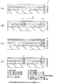
- 支持基板上に、第1埋め込み酸化膜、第1単結晶シリコン層、第2埋め込み酸化膜、及び第2単結晶シリコン層が順に積層された2重SOI基板を用意する工程と、
前記2重SOI基板のバイポーラトランジスタ被形成領域を画成する領域に対して、前記第2単結晶シリコン層の表面から前記第1埋め込み酸化膜の表面が露出する深さにまでエッチングを行って、ディープトレンチを形成する工程と、
前記2重SOI基板上に、シリコン窒化膜及びシリコン酸化膜を順に積層して、前記ディープトレンチを埋め込む工程と、
前記バイポーラトランジスタ被形成領域に、前記第2埋め込み酸化膜の表面が露出する深さにまでエッチングを行って開口部を設ける工程と、
前記バイポーラトランジスタ被形成領域内の前記第2埋め込み酸化膜を、ウェットエッチングにより除去して空孔部を設ける工程と、
前記開口部及び前記空孔部に、バイポーラトランジスタのコレクタとなる、第1導電型不純物が高濃度にドープされた多結晶シリコン層を堆積する工程と、
前記第2単結晶シリコン層と電気的に接続されるベース電極を形成する工程と、
前記バイポーラトランジスタ被形成領域の前記第2単結晶シリコン層上に、エピタキシャル成長シリコン層を形成し、前記第2単結晶シリコン層の前記エピタキシャル成長シリコン層と接する部分に第2導電型導電層を形成する工程と、
前記エピタキシャル成長シリコン層と、該エピタキシャル成長シリコン層と接する、前記第2導電型導電層の一部分にエミッタを形成するとともに、前記第2導電型導電層の他の部分にベースを形成する工程と、
前記ベース電極と前記第2単結晶シリコン層を介して電気的に接続されるエミッタ電極を形成する工程と
を備えることを特徴とする半導体装置の製造方法。 - 支持基板上に、第1埋め込み酸化膜、第1単結晶シリコン層、第2埋め込み酸化膜、及び第2単結晶シリコン層が順に積層された2重SOI基板を用意する工程と、
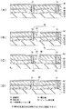
前記2重SOI基板のバイポーラトランジスタ被形成領域を画成する領域に対して、前記第2単結晶シリコン層の表面から前記第1埋め込み酸化膜の表面が露出する深さにまでエッチングを行って、ディープトレンチを形成する工程と、
前記2重SOI基板上に、シリコン窒化膜及びシリコン酸化膜を順に積層して、前記ディープトレンチを埋め込む工程と、
前記バイポーラトランジスタ被形成領域に、前記第2埋め込み酸化膜の表面が露出する深さにまでエッチングを行って開口部を設ける工程と、
前記バイポーラトランジスタ被形成領域内の前記第2埋め込み酸化膜を、ウェットエッチングにより除去して空孔部を設ける工程と、
前記空孔部を、バイポーラトランジスタのコレクタとなる、第1導電型不純物が高濃度にドープされた多結晶シリコン層で埋め込む工程と、
前記開口部をメタルで埋め込む工程と、
前記第2単結晶シリコン層と電気的に接続されるベース電極を形成する工程と、
前記バイポーラトランジスタ被形成領域の前記第2単結晶シリコン層上に、エピタキシャル成長シリコン層を形成し、前記第2単結晶シリコン層の前記エピタキシャル成長シリコン層と接する部分に第2導電型導電層を形成する工程と、
前記エピタキシャル成長シリコン層と、該エピタキシャル成長シリコン層と接する、前記第2導電型導電層の一部分にエミッタを形成するとともに、前記第2導電型導電層の他の部分にベースを形成する工程と、
前記ベース電極と前記第2単結晶シリコン層を介して電気的に接続されるエミッタ電極を形成する工程と
を備えることを特徴とする半導体装置の製造方法。 - さらに、
前記第2単結晶シリコン層の、前記バイポーラトランジスタ被形成領域及び前記ディープトレンチが形成された領域以外の領域に、MOSFET被形成領域を画成する素子分離酸化膜を形成する工程と、
前記MOSFET被形成領域にMOSFETを形成する工程と
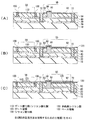
を備えることを特徴とする請求項1又は2に記載の半導体装置の製造方法。 - 支持基板上に、第1埋め込み酸化膜、第1単結晶シリコン層、第2埋め込み酸化膜、第2単結晶シリコン層を順に積層して構成される2重SOI基板に形成されていて、前記第1埋め込み酸化膜に達するディープトレンチで画成されたバイポーラトランジスタ被形成領域に形成されたバイポーラトランジスタを備える半導体装置であって、
前記バイポーラトランジスタは、
前記バイポーラトランジスタ被形成領域の、前記第1単結晶シリコン層及び前記第2単結晶シリコン層の間を埋め込むように、かつ、前記第2単結晶シリコン層を貫通するように形成された、前記バイポーラトランジスタのコレクタとなる、第1導電型不純物が高濃度にドープされた多結晶シリコン層と、
前記バイポーラトランジスタ被形成領域の前記第2単結晶シリコン層上に形成されたエピタキシャル成長シリコン層と、
前記第2単結晶シリコン層の前記エピタキシャル成長シリコン層と接する部分に形成された第2導電型導電層と、
前記エピタキシャル成長シリコン層と、該エピタキシャル成長シリコン層と接する、前記第2導電型導電層の一部分に形成されたエミッタと、
前記第2導電型導電層の他の部分に形成されたベースと
を備えることを特徴とする半導体装置。 - 支持基板上に、第1埋め込み酸化膜、第1単結晶シリコン層、第2埋め込み酸化膜、第2単結晶シリコン層を順に積層して構成される2重SOI基板に形成されていて、前記第1埋め込み酸化膜に達するディープトレンチで画成されたバイポーラトランジスタ被形成領域に形成されたバイポーラトランジスタを備える半導体装置であって、
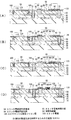
前記バイポーラトランジスタは、
前記バイポーラトランジスタ被形成領域の、前記第1単結晶シリコン層及び前記第2単結晶シリコン層の間を埋め込むように形成された、第1導電型不純物が高濃度にドープされた多結晶シリコン層と、
前記第2単結晶シリコン層を貫通するように、前記多結晶シリコン層と電気的に接続するように形成されたメタルと、
前記バイポーラトランジスタ被形成領域の前記第2単結晶シリコン層上に形成されたエピタキシャル成長シリコン層と、
前記第2単結晶シリコン層の前記エピタキシャル成長シリコン層と接する部分に形成された第2導電型導電層と、
前記エピタキシャル成長シリコン層と、該エピタキシャル成長シリコン層と接する、前記第2導電型導電層の一部分に形成されたエミッタと、
前記第2導電型導電層の他の部分に形成されたベースと
を備えることを特徴とする半導体装置。 - 前記ディープトレンチが形成された領域、及び、前記ディープトレンチで画成された領域以外の前記第2単結晶シリコン層の領域部分に形成された素子分離酸化膜と、
前記素子分離酸化膜で画成された領域に形成されたMOSFETと
を備えることを特徴とする請求項4又は5に記載の半導体装置。
Priority Applications (3)
| Application Number | Priority Date | Filing Date | Title |
|---|---|---|---|
| JP2004246374A JP4845357B2 (ja) | 2004-08-26 | 2004-08-26 | 半導体装置とその製造方法 |
| US11/191,190 US7205587B2 (en) | 2004-08-26 | 2005-07-28 | Semiconductor device and method of producing the same |
| US11/638,551 US7285455B2 (en) | 2004-08-26 | 2006-12-14 | Method of producing the same |
Applications Claiming Priority (1)
| Application Number | Priority Date | Filing Date | Title |
|---|---|---|---|
| JP2004246374A JP4845357B2 (ja) | 2004-08-26 | 2004-08-26 | 半導体装置とその製造方法 |
Publications (3)
| Publication Number | Publication Date |
|---|---|
| JP2006066577A JP2006066577A (ja) | 2006-03-09 |
| JP2006066577A5 JP2006066577A5 (ja) | 2007-01-18 |
| JP4845357B2 true JP4845357B2 (ja) | 2011-12-28 |
Family
ID=35943851
Family Applications (1)
| Application Number | Title | Priority Date | Filing Date |
|---|---|---|---|
| JP2004246374A Expired - Fee Related JP4845357B2 (ja) | 2004-08-26 | 2004-08-26 | 半導体装置とその製造方法 |
Country Status (2)
| Country | Link |
|---|---|
| US (2) | US7205587B2 (ja) |
| JP (1) | JP4845357B2 (ja) |
Families Citing this family (19)
| Publication number | Priority date | Publication date | Assignee | Title |
|---|---|---|---|---|
| JP2006128428A (ja) * | 2004-10-29 | 2006-05-18 | Seiko Epson Corp | 半導体基板、半導体装置、半導体基板の製造方法および半導体装置の製造方法 |
| JP2006156867A (ja) * | 2004-12-01 | 2006-06-15 | Seiko Epson Corp | 半導体基板の製造方法および半導体装置の製造方法 |
| US7986029B2 (en) * | 2005-11-08 | 2011-07-26 | Taiwan Semiconductor Manufacturing Company, Ltd. | Dual SOI structure |
| US7799592B2 (en) * | 2006-09-27 | 2010-09-21 | Taiwan Semiconductor Manufacturing Company, Ltd. | Tri-gate field-effect transistors formed by aspect ratio trapping |
| US8115254B2 (en) * | 2007-09-25 | 2012-02-14 | International Business Machines Corporation | Semiconductor-on-insulator structures including a trench containing an insulator stressor plug and method of fabricating same |
| US7829971B2 (en) * | 2007-12-14 | 2010-11-09 | Denso Corporation | Semiconductor apparatus |
| US20090201678A1 (en) * | 2008-02-08 | 2009-08-13 | Raley Jay F | Heat sink for semiconductor light sources |
| JP4894910B2 (ja) * | 2009-01-15 | 2012-03-14 | 株式会社デンソー | 半導体装置の製造方法及び半導体装置並びにその半導体装置を内蔵する多層基板 |
| US8093084B2 (en) | 2009-04-30 | 2012-01-10 | Freescale Semiconductor, Inc. | Semiconductor device with photonics |
| CN102280451B (zh) * | 2010-06-13 | 2014-03-19 | 中芯国际集成电路制造(上海)有限公司 | 半导体器件及其制作方法 |
| US8809156B1 (en) | 2013-01-25 | 2014-08-19 | International Business Machines Corporation | Method for implementing deep trench enabled high current capable bipolar transistor for current switching and output driver applications |
| US9466536B2 (en) * | 2013-03-27 | 2016-10-11 | Qualcomm Incorporated | Semiconductor-on-insulator integrated circuit with back side gate |
| US8748245B1 (en) | 2013-03-27 | 2014-06-10 | Io Semiconductor, Inc. | Semiconductor-on-insulator integrated circuit with interconnect below the insulator |
| US9478507B2 (en) | 2013-03-27 | 2016-10-25 | Qualcomm Incorporated | Integrated circuit assembly with faraday cage |
| CN103426828A (zh) * | 2013-07-12 | 2013-12-04 | 上海新储集成电路有限公司 | 一种基于绝缘体上硅材料的双极型高压cmos单多晶硅填充深沟道器件隔离工艺 |
| US9431339B2 (en) | 2014-02-19 | 2016-08-30 | International Business Machines Corporation | Wiring structure for trench fuse component with methods of fabrication |
| US9311442B2 (en) | 2014-04-25 | 2016-04-12 | Globalfoundries Inc. | Net-voltage-aware optical proximity correction (OPC) |
| CN105097851A (zh) * | 2014-05-04 | 2015-11-25 | 中芯国际集成电路制造(上海)有限公司 | 一种cmos图像传感器及其制造方法和电子装置 |
| CN112331673A (zh) * | 2019-08-05 | 2021-02-05 | 广东美的白色家电技术创新中心有限公司 | 一种半导体芯片以及智能功率模块 |
Family Cites Families (10)
| Publication number | Priority date | Publication date | Assignee | Title |
|---|---|---|---|---|
| JPH01189154A (ja) * | 1988-01-25 | 1989-07-28 | Hitachi Ltd | 半導体装置及びその製造方法 |
| US5212397A (en) * | 1990-08-13 | 1993-05-18 | Motorola, Inc. | BiCMOS device having an SOI substrate and process for making the same |
| JPH0669430A (ja) | 1992-08-18 | 1994-03-11 | Fujitsu Ltd | 半導体装置の製造方法 |
| JP3644980B2 (ja) * | 1993-09-06 | 2005-05-11 | 株式会社ルネサステクノロジ | 半導体装置の製造方法 |
| US5583368A (en) * | 1994-08-11 | 1996-12-10 | International Business Machines Corporation | Stacked devices |
| US6013936A (en) * | 1998-08-06 | 2000-01-11 | International Business Machines Corporation | Double silicon-on-insulator device and method therefor |
| US6521974B1 (en) * | 1999-10-14 | 2003-02-18 | Hitachi, Ltd. | Bipolar transistor and manufacturing method thereof |
| JP2001274234A (ja) * | 2000-03-27 | 2001-10-05 | Matsushita Electric Ind Co Ltd | 半導体装置およびその製造方法 |
| DE10138648A1 (de) * | 2001-08-07 | 2003-03-06 | Infineon Technologies Ag | Verfahren zum parallelen Herstellen eines MOS-Transistors und eines Bipolartransistors |
| US6936910B2 (en) * | 2003-05-09 | 2005-08-30 | International Business Machines Corporation | BiCMOS technology on SOI substrates |
-
2004
- 2004-08-26 JP JP2004246374A patent/JP4845357B2/ja not_active Expired - Fee Related
-
2005
- 2005-07-28 US US11/191,190 patent/US7205587B2/en not_active Expired - Fee Related
-
2006
- 2006-12-14 US US11/638,551 patent/US7285455B2/en not_active Expired - Fee Related
Also Published As
| Publication number | Publication date |
|---|---|
| JP2006066577A (ja) | 2006-03-09 |
| US20070090400A1 (en) | 2007-04-26 |
| US20060046409A1 (en) | 2006-03-02 |
| US7285455B2 (en) | 2007-10-23 |
| US7205587B2 (en) | 2007-04-17 |
Similar Documents
| Publication | Publication Date | Title |
|---|---|---|
| US7205587B2 (en) | Semiconductor device and method of producing the same | |
| CN106206697B (zh) | 绝缘体上硅(soi)衬底上的横向双极结型晶体管(bjt) | |
| JP2004064063A (ja) | 高電圧縦型dmosトランジスタ及びその製造方法 | |
| JP2010010456A (ja) | 半導体装置 | |
| JP4138806B2 (ja) | バイポーラトランジスタの形成方法 | |
| JP2004274023A (ja) | 強い導電埋込層を備えた集積回路 | |
| JP2013545306A (ja) | 拡張されたドレインmosトランジスタ | |
| US20110281411A1 (en) | Method for manufacturing semiconductor device | |
| KR100854077B1 (ko) | 웨이퍼 본딩을 이용한 soi 기판 제조 방법과 이 soi기판을 사용한 상보형 고전압 바이폴라 트랜지스터 제조방법 | |
| JP4402953B2 (ja) | 半導体装置の製造方法 | |
| JP2001044399A (ja) | 半導体装置の製造方法 | |
| KR100249022B1 (ko) | 반도체장치의 소자 격리 방법 | |
| JP2007081167A (ja) | 半導体装置の製造方法 | |
| KR20060062487A (ko) | 바이폴라 트랜지스터 및 그 제조방법 | |
| JP5277555B2 (ja) | 半導体装置の製造方法 | |
| JP2006066573A (ja) | 半導体装置および半導体装置の製造方法 | |
| JP4947692B2 (ja) | 半導体装置の製造方法及び半導体装置 | |
| JP2009252814A (ja) | 半導体装置の製造方法及び半導体装置 | |
| JPH10270544A (ja) | 半導体装置およびその製造方法 | |
| JP2002334889A (ja) | 半導体装置およびその製造方法 | |
| JP2007266390A (ja) | 半導体装置の製造方法 | |
| KR20050065139A (ko) | 반도체 소자의 소자 분리막 및 그의 형성 방법 | |
| JP2007173451A (ja) | バイポーラトランジスタおよびその製造方法 | |
| JP2005136338A (ja) | 半導体装置及びその製造方法 | |
| JP2004304100A (ja) | 半導体装置及びその製造方法 |
Legal Events
| Date | Code | Title | Description |
|---|---|---|---|
| A521 | Written amendment |
Free format text: JAPANESE INTERMEDIATE CODE: A523 Effective date: 20061124 |
|
| A621 | Written request for application examination |
Free format text: JAPANESE INTERMEDIATE CODE: A621 Effective date: 20061124 |
|
| A977 | Report on retrieval |
Free format text: JAPANESE INTERMEDIATE CODE: A971007 Effective date: 20080826 |
|
| A711 | Notification of change in applicant |
Free format text: JAPANESE INTERMEDIATE CODE: A712 Effective date: 20081126 |
|
| RD03 | Notification of appointment of power of attorney |
Free format text: JAPANESE INTERMEDIATE CODE: A7423 Effective date: 20090204 |
|
| A131 | Notification of reasons for refusal |
Free format text: JAPANESE INTERMEDIATE CODE: A131 Effective date: 20101116 |
|
| A521 | Written amendment |
Free format text: JAPANESE INTERMEDIATE CODE: A523 Effective date: 20110117 |
|
| TRDD | Decision of grant or rejection written | ||
| A01 | Written decision to grant a patent or to grant a registration (utility model) |
Free format text: JAPANESE INTERMEDIATE CODE: A01 Effective date: 20110920 |
|
| A01 | Written decision to grant a patent or to grant a registration (utility model) |
Free format text: JAPANESE INTERMEDIATE CODE: A01 |
|
| A61 | First payment of annual fees (during grant procedure) |
Free format text: JAPANESE INTERMEDIATE CODE: A61 Effective date: 20111011 |
|
| FPAY | Renewal fee payment (event date is renewal date of database) |
Free format text: PAYMENT UNTIL: 20141021 Year of fee payment: 3 |
|
| R150 | Certificate of patent or registration of utility model |
Free format text: JAPANESE INTERMEDIATE CODE: R150 |
|
| S531 | Written request for registration of change of domicile |
Free format text: JAPANESE INTERMEDIATE CODE: R313531 |
|
| R350 | Written notification of registration of transfer |
Free format text: JAPANESE INTERMEDIATE CODE: R350 |
|
| LAPS | Cancellation because of no payment of annual fees |